City, University of London Institutional Repository
Citation
:
Jones, K., Kim, J. and Horowitz, M. (2010). Fast, non-monte-carlo estimation of transient performance variation due to device mismatch. IEEE Transactions on Circuits and Systems, 57(7), pp. 1746-1755. doi: 10.1109/TCSI.2009.2035418This is the unspecified version of the paper.
This version of the publication may differ from the final published
version.
Permanent repository link:
http://openaccess.city.ac.uk/1968/Link to published version
:
http://dx.doi.org/10.1109/TCSI.2009.2035418Copyright and reuse:
City Research Online aims to make research
outputs of City, University of London available to a wider audience.
Copyright and Moral Rights remain with the author(s) and/or copyright
holders. URLs from City Research Online may be freely distributed and
linked to.
City Research Online: http://openaccess.city.ac.uk/ [email protected]
Abstract—This paper describes an efficient way of simulating the effects of device random mismatch on circuit transient characteristics, such as variations in delay or in frequency. The proposed method models DC random offsets as equivalent AC pseudo-noises and leverages the fast, linear periodically time-varying (LPTV) noise analysis available from RF circuit simulators. Therefore, the method can be considered as an extension to DC match analysis and offers a large speed-up compared to the traditional Monte-Carlo analysis. Although the assumed linear perturbation model is valid only for small variations, it enables easy ways to estimate correlations among variations and identify the most sensitive design parameters to mismatch, all at no additional simulation cost. Three benchmarks measuring the variations in the input offset voltage of a clocked comparator, the delay of a logic path, and the frequency of an oscillator demonstrate the speed improvement of about 100-1000
compared to a 1000-point Monte-Carlo method.
Index Terms— circuit simulation, mismatch, sensitivity analysis, Monte-Carlo analysis, variability, yield.
I. INTRODUCTION
S CMOS device mismatch nearly doubles for every process generation below 100nm and the 3-variation of the transistor drive current reaches beyond 30% [1], analyzing its impacts on circuit performance and yield becomes increasingly more important. With such large variations in device characteristics, the traditional worst-case design approaches result in excessive design margins and unnecessarily sacrifice key performances such as speed, power, and area [2],[3]. To avoid such excessive margins and retain high performance, a statistical approach to analyzing the circuit performance is necessary. This paper describes an efficient method of simulating the impact of device mismatch on various transient characteristics [6], which can greatly relax the computational burden when optimizing circuit designs for yield.
Manuscript received December 9, 2008; revised June 20, 2009.
J. Kim is with Stanford University, Stanford, CA 94305, USA (phone: 650-725-6599; fax: 650-725-3383; e-mail: [email protected]). He was with Rambus, Inc., Los Altos, CA 94022, USA.
K. D. Jones is with Green Plug, Inc., San Ramon, CA 94583 (e-mail: [email protected]). He was with Rambus, Inc., Los Altos, CA 94022, USA.
M. A. Horowitz is with Department of Electrical Engineering, Stanford University, Stanford, CA 94305, USA and is also with Rambus, Inc., Los Altos, CA 94022, USA (e-mail: [email protected]).
The most common way of estimating the statistical distribution of circuit performance is Monte-Carlo analysis. Device mismatch is modeled as a set of randomly generated samples that represent the probability distributions of the device parameters. The circuit is then repetitively simulated with the random device samples and the statistics of the resulting performance are collected. While it is conceptually very simple, Monte-Carlo analysis requires a large number of samples in order to estimate the performance statistics reliably; typically, over hundreds to thousands of circuit simulations are needed for the moderate accuracy of ±5~15%. It can be particularly costly for long transient simulations where the circuits have to reach to a steady-state behavior before the performance of interest can be measured.
Numerous methods were therefore reported in literature that reduce the computational cost of the Monte-Carlo analysis [4],[5]. For example, variance reduction techniques including importance sampling, stratified sampling, correlated sampling, and regression sampling can improve the precision of the statistical estimate with a smaller set of random simulations. Also, statistical regression techniques such as response surface modeling (RSM) have been applied to further reduce the number of random simulations. However, the computational cost still remains high for large-scale circuits.
This paper focuses on ways to estimate the effects of device mismatch using linear sensitivity analysis. Most transistor-level circuit simulators including SPICE offer an analysis mode where it calculates the sensitivity of a DC voltage or current with respect to small variations in device parameters (.SENS) [20],[26]. This sensitivity analysis is a low-cost computation yet its results can be used to effectively estimate the yield. For example, Schenkel, et al. [7] combined the sensitivity analysis and a search algorithm to identify the transistor pairs that are most sensitive to mismatch. Oehm and Schumacher [8] calculated the mismatch effects on the DC operating point of a circuit by scaling each mismatch distribution by the corresponding sensitivity and combining them via root-mean-square summation, assuming that each mismatch distribution is an independent Gaussian with small variance. Some commercial simulators including Spectre and HSPICE offer a similar analysis called DC match analysis [9], which is found effective in estimating the mismatch effects on DC characteristics of various analog circuits, such as the offset voltage of an operational amplifier, the output voltage of a bandgap reference circuit, or static noise margin of SRAM
Fast, Non-Monte-Carlo Estimation of Transient
Performance Variation Due to Device Mismatch
Jaeha Kim, Member, IEEE , Kevin D. Jones, Member, IEEE, and Mark A. Horowitz, Fellow, IEEE
memory cells.
However, no equivalent approach to estimate the variation in transient characteristics has been reported prior to [6]. The examples of transient characteristics include skews in a clock distribution network, frequency of an oscillator, and nonlinearity of an A/D converter, which can only be measured via time-domain, transient simulations. While algorithms for transient sensitivity analysis exist, the computational cost for large circuits with many mismatch variables is still very high. Hocevar, et al. [10] used transient sensitivities to estimate yield gradients but limited the number of mismatch parameters to four by modeling the die-to-die variation only.
This paper extends the idea of Oehm and Schumacher [8] and analyzes the variations in the transient characteristics via linear sensitivity analysis in more depth than it was in [6]. It asserts that the sensitivity-based mismatch analysis for transient characteristics can be most efficiently carried out when using a linear, periodically time-varying (LPTV) sensitivity analysis [22] rather than using the transient sensitivity analysis [23]. In order to leverage the existing RF circuit simulators such as SpectreRF or ADS, we model the device mismatch as low-frequency pseudo-noise using Verilog-A analog behavioral description language and use the LPTV noise analysis in place of the LPTV sensitivity analysis. The linear perturbation model assumed by the proposed mismatch analysis makes it easy to model and analyze correlations among circuit response variations and to determine the sensitivity of the performance variation with respect to each design parameter. Both the correlations and mismatch sensitivities can be calculated at no additional simulation cost
whereas the equivalent information would cost linear computational time with the number of random parameters in other sampling-based mismatch analyses. In particular, the sensitivities of the performance variation to design parameters are the essential information when optimizing circuits for yield. This paper is organized as follows. First, it outlines the sensitivity-based mismatch analysis based on LPTV noise analysis (Section II) and the subsequent sections describe the various aspects of applying the method to common circuits such as the clocked comparators, logic paths, and oscillators (Sections III, IV, and V). Section VI then discusses the benchmark results that demonstrate about 100-1000 speed-up compared to a 1000-point Monte-Carlo simulation and Section VII addresses some limitations of the described mismatch analysis.
II. SENSITIVITY-BASED MISMATCH ANALYSIS VIA LPTV NOISE SIMULATION
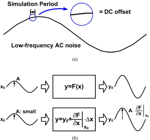
One of our basic ideas is that the random device mismatch (i.e. DC offsets) and low-frequency AC noise have indistinguishable effects on the circuit response if they are observed over a bounded period of time. Fig. 1(a) illustrates this idea conceptually. When the simulation time is bounded, we can always come up with low enough frequency AC noise that appears virtually fixed during the observation period. Therefore, we can analyze the effects of DC mismatch by simulating the effects of the equivalent AC noise instead. Interestingly, Galup-Montoro, et al. [24] demonstrated that the model equations for the transistor current mismatch can be derived based on the carrier number fluctuation theory which underlies the 1/f flicker noise. In essence, the mismatch and the 1/f flicker noise may share the same physical explanations except that one is spatial fluctuation while the other is temporal.
Another insight is that the small-signal noise analysis based on linear perturbation model is far more efficient than a general, nonlinear noise analysis (e.g. Monte-Carlo) and the results can be as accurate if the noise is sufficiently small or the system is linear. Fig. 1(b) compares these two approaches conceptually. Let’s assume that we have to evaluate a response of a memoryless system y=F(x) to a sinusoidal input centered at x0 with an amplitude A. A general, nonlinear approach would have to evaluate the system function y=F(x) for virtually all possible input values. However, if we can assume that the input amplitude A is sufficiently small, we can treat the system as linear and carry out a small-signal linear analysis. In this case, the output can be approximated as a sinusoid centered at
y0=F(x0) and only its amplitude needs to be computed, which is simply the input amplitude A scaled by the linearized transfer gain of the system (i.e. sensitivity) at the nominal input of x0.
The previous DC sensitivity-based mismatch analyses in [8],[9] can be considered equivalent to performing a small-signal noise analysis if we apply the proper translations between the mismatch variances and the noise power-spectral densities (PSD’s). For instance, consider a sensitivity-based
(a)
[image:3.612.48.298.449.682.2](b)
mismatch analysis described in [8], where the variation in DC voltage or current is estimated as:
i i i out2 S2 2
(1)
where i2 is the variance in the i-th device parameter distribution and Si is the DC sensitivity of the DC voltage or current being measured with respect to the i-th device parameter. It is based on the linear perturbation model where the change in the output parameter of interest (Pout) can be expressed as a sum of the input parameter changes (Pi’s) scaled by their sensitivities (Si’s), respectively. In equation,
i i i
out S P
P . (2)
And the expression in (1) assumes that the variations in the parameters (Pi’s) are independent of one another. On the other hand, the small-signal noise analysis such as .NOISE in SPICE derives the output noise PSD via a similarly-looking equation to (1):
i
i i
out f TF f PSD f
PSD ( ) ( )2 ( ) (3)
where PSDi(f) is the power-spectral density of the i-th noise source and TFi(f) is the frequency-domain transfer function of the circuit between the i-th noise source and the output. Therefore, if we assume that we can approximate the DC sensitivities (Si’s) with the low-frequency transfer gains (e.g.
TFi(f)’s at f=1-Hz), then one can perform a DC sensitivity-based mismatch analysis using a small-signal noise simulation by inserting the pseudo-noise sources whose
PSDi(f)’s are proportional to i2’s, respectively, and interpreting the simulated PSDout(f) as the measured variation out2. It is not surprising since both analyses are based on the
principle of linear, adjoint sensitivity analysis [25].
Then it becomes apparent that a natural way of extending the DC sensitivity-based mismatch analysis in [8],[9] to measure the variations in transient characteristics is to perform a small-signal, yet time-varying noise analysis instead of the linear, time-invariant noise analysis. There exist largely two categories of such time-varying noise analyses in literature. One is the transient noise analysis [18] which does not assume any periodicity in the circuit response and the other is the linear periodically time-varying (LPTV) noise analysis which requires a periodic steady-state response of the circuit. We will compare these two noise analyses in more detail in Section IV and assert that the LPTV noise analysis is the more efficient method.
III. MODELING MISMATCH AS LOW-FREQUENCY
PSEUDO-NOISE
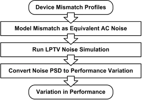
The overall flow of the proposed mismatch analysis is illustrated in Fig. 2. The first step in the proposed mismatch analysis is to convert the device parameter mismatches to the equivalent AC pseudo-noise sources. In general, the pseudo-noise should have a power that is proportional to the variance of the mismatch distribution.
In LPTV noise analysis, the noise at high frequency may be converted down to a lower frequency, due to the phenomenon called noise folding [13]. Therefore, it is necessary to keep the high-frequency PSD of the pseudo-noise low and to prevent noise folding from contaminating the true mismatch-induced effects. Flicker noise has a 1/f PSD and is the simplest low-frequency noise source to implement using an analog behavioral description language like Verilog-A.
[image:4.612.317.554.518.686.2]In the following examples, a mismatch with variance of 2 is converted to a 1/f-flicker noise with a PSD equal to 2 at 1-Hz (i.e. N2/f = 2/f). The choice of 1-Hz as the pseudo-noise frequency point is arbitrary as it only needs to be sufficiently
[image:4.612.57.290.549.713.2]Fig. 2. The proposed sensitivity-based mismatch analysis flow.
Fig. 3. The equivalent pseudo-noise representation for the variations in resistance (R), capacitance (C), and inductance (L). R0, C0, and L0 denote the nominal values and R2, C2, and L2 denote the variances of R, C, and L,
lower than the fundamental frequency of the LPTV noise analysis.
A. Mismatch in Passive Devices
Passive devices may have uncertainties in their resistance, capacitance, or inductance. Since a typical circuit simulator can only handle noise sources in voltage or current, these parameter variations have to be translated to the equivalent pseudo-noise sources in voltage or current. Fig. 3 shows examples of the equivalent pseudo-noise sources for modeling mismatches in a resistor, a capacitor, and an inductor. For example, the pseudo voltage noise representing the resistance mismatch has a PSD of R2·IR2 at 1-Hz, where R2 is the variance of the resistance mismatch and IR is the nominal current flowing through the resistor. Similarly, the pseudo-noise powers for the capacitance and inductance mismatches have the additional dependencies on either the voltage across or the current flowing through the elements. These bias dependencies can be modeled using Verilog-A.
B. Mismatch in MOS Transistors
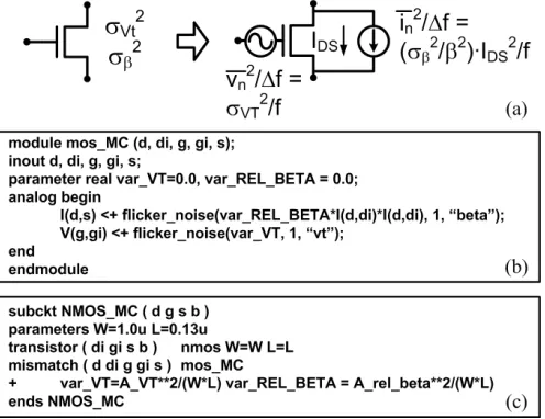
Mismatch in MOSFET devices can also be modeled with pseudo-noises. In the example of the Pelgrom model [11], the transistor mismatch is modeled as the uncertainties in the threshold voltage (VT) and the current factor (), where their variances are inversely proportional to the gate area. In equations,
VT2 = AVT2/(W·L) (4)
2/2 = A2/(W·L) (5)
where W is the width and L is the length of the transistor. AVT
and A are constants specific to the process technology. Fig. 4(a) shows the schematic diagram of the pseudo-noise sources that model the mismatches in VT and . The mismatch in VT is translated to a voltage noise source at the gate node with PSD of VT2 at 1-Hz. The mismatch in is translated to a current noise source across the drain and source with PSD of (2/2)·IDS2 at 1-Hz. Fig. 4(b) and (c) list the Verilog-A codes for these pseudo-noise sources and an example of embedding them within the transistor model.
Note that we can also model the variations in other transistor parameters than VT and using the pseudo-noise sources. For example, ref. [28] proposed a modified mismatch model that includes the variations in the body effect constant () and in the mobility degradation constant (). Ref. [29] described a model that expresses the mismatch in terms of basic physical parameters such as the sheet resistance, channel dopant concentration, carrier mobility, and gate oxide thickness. Virtually all mismatch models for MOSFETs express the variation in the drain current as some function of random parameters, which is typically bias-dependent. Those bias-dependent equations with random parameters can be easily translated into Verilog-A description with pseudo-noise sources as in the Pelgrom model example in Fig. 5.
C. Modeling Correlations
The mismatches in different parameters may be correlated, for example, spatially within a die or wafer. Without taking correlations into account, one can get misleading estimate on the mismatch effects. For example, by assuming that the gates in the local logic path have independent variations in delay, one can over-estimate the minimum total delay while under-estimating the maximum total delay, none of which is desirable for the reliable timing closure.
While all noise sources modeled in Verilog-A are assumed independent of one another, one can construct correlated noise sources by linearly combining the independent noise sources. For example, assume that X1, X2, …, XN are independent noise sources with variance of 1 and mean of 0. It is well known that a set of correlated noise sources Y1, Y2, …, YM constructed as linear combinations of Xj’s, that is, Yi = aijXj, for i=1, 2, …,
M, have a covariance matrix C expressed as:
C = AAT (6)
where A is an M-by-N matrix of {aij}’s and AT denotes the transpose of the matrix A. Therefore, one can construct the desired correlated noise sources by choosing a proper set of coefficients A={aij}’s.
IV. LPTVCYCLOSTATIONARY NOISE SIMULATION
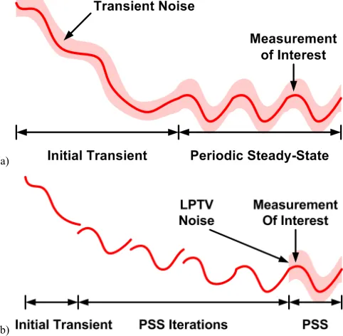
The next step is to simulate the circuits with the pseudo-noise sources. While algorithms exist that can simulate the noise in transient responses [18], they are compute-intensive and
Fig. 4. (a) The equivalent pseudo-noises for modeling MOS transistor mismatch, (b) Verilog-A code example, (c) Spectre example of embedding the pseudo-noise sources inside the transistor model. Note that var_REL_BETA
[image:5.612.51.299.494.685.2]especially inefficient for circuits that need to be simulated for a long period before the performance can be measured. Much of the computation is wasted on simulating the noise response during the settling period, which is of no interest (see Fig. 5).
The LPTV noise analysis, also referred to as the periodic noise (PNOISE) analysis offered by RF circuit simulators such as SpectreRF and ADS, provides a more efficient way of simulating the effects of these pseudo-noise sources [12]-[17]. First, the initial settling transient is simulated only once and the final steady-state response is found by an iterative search such as shooting Newton or harmonic balance algorithms [12], rather than by a brute-force, long transient simulation. This steady-state response can be periodic if not constant (i.e. DC). Second, the small-signal noise analysis is performed only on this steady-state response, which linearizes the circuit around its periodic steady-state response and calculates the output noise PSD quickly based on the linear, periodically time-varying (LPTV) system analysis [12]-[14]. Moreover, Krylov subspace algorithms like [16],[17] further reduce the computational effort and make the LPTV noise analysis applicable to large-scale circuits.
However, the LPTV analysis requires that the circuit have a periodic steady state. For mismatch analysis, it is also required that the performance of interest be measurable from the steady state, since it is the only response of which variations due to the pseudo-noises are simulated. While not all circuits have periodic steady states, many can be made periodic with proper testbench configurations. The following subsections discuss a few practical examples.
A. Input Offset Voltage of Clocked Comparator
A clocked comparator is a circuit that makes decision as to whether the input signal is high or low at every clock cycle. Most clocked comparators use regenerative circuits to achieve a high amplification gain via positive feedback. Clocked comparators have widespread use in many applications where digital information needs to be recovered from analog signals, such as analog-to-digital converters, wireline receivers, and memory bit-line detectors.
[image:6.612.54.295.433.669.2]We look at a problem of measuring the variation in the input-referred offset of a clocked comparator. Unlike measuring the input-referred offset of a linear amplifier, that of a clocked comparator cannot be measured via DC analysis in SPICE. The comparator has no stable DC operating point from which the offset voltage can be measured. Moreover, the input offset may be influenced by the transient effects such as kick-back noise. Thus, the input offset voltage can only be measured via transient simulation. Typically, the input voltage is swept until one finds a value that puts the comparator in a metastable state, the state in which the comparator cannot resolve its decision in a finite period. However, this sweep-based measurement does not fit into our mismatch analysis approach, where the LPTV noise simulation requires a periodic steady state of the comparator from which the input offset voltage can be measured.
Fig. 6 shows a configuration in which the comparator converges to a metastable state as it reaches to its periodic steady state. Any difference between the two differential output voltages builds up a voltage VOS that adjusts the offset applied to the input. As the simulation progresses in time, the
(a)
(b)
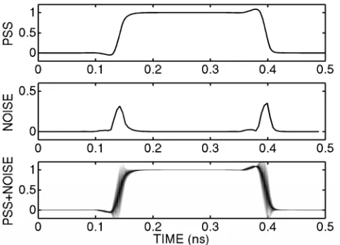
[image:6.612.321.552.445.559.2]Fig. 5. Two time-varying noise simulation methods available for measuring the variations in circuit transient responses via the proposed pseudo-noise based analysis: (a) transient noise analysis [18] and (b) LPTV noise analysis [12]-[14]. If the measurement of interest is to be taken from the circuit’s periodic steady state (PSS), the LPTV noise analysis is the more efficient method as it simulates the noise effects only on the PSS.
[image:6.612.322.549.608.706.2]Fig. 6. Simulation testbench configuration for measuring the input offset voltage of a clocked comparator. Once converged to its periodic steady state, the comparator becomes metastable and VOS indicates the input offset.
comparator settles to a point where the two outputs are no longer different, i.e. the metastable state. The steady state of this configuration is periodic with the clock period and the final
VOS indicates the input offset voltage of the comparator.
B. Delay of Logic Path
The delay variation of a logic path or a clock distribution network is of great importance to synchronous digital system designs. This example tries to address this class of problems with a simple logic path shown in Fig. 7.
Setting up a periodic steady state for this logic path is easy; simply apply periodic or constant signals to all the inputs. The period T should be equal for all the periodic inputs and should be long enough for the signals not to interfere across the period boundary. The circuit then has a periodic steady-state with a fundamental frequency equal to 1/T.
C. Frequency of Oscillator
When measuring the variation in the frequency of an oscillator, no special setup is necessary since the oscillator is inherently a periodic system. However, an oscillator is unique in that its fundamental frequency is not known a priori and may change due to mismatch. RF simulators use dedicated algorithms to find the periodic steady state and to perform the noise analysis for oscillators [15].
These examples provide clues on how one might devise a periodic simulation setup to measure the performance variation of his/her interest when the circuit under test is not periodic or when the performance of interest is not measured from the steady-state. If the performance can be measured from a single time-domain simulation with a finite time span, such as the delay in the logic path example, then a periodic setup can simply be the one that periodically repeats the original simulation. If the performance is to be measured based on a search over multiple test cases, such as the input-referred offset
in the comparator example, then additional effort might be necessary to first create a testbench that can perform the search in a single simulation run. A brute-force approach could be to expand all the test cases and measure them all at once in a single simulation run (e.g. simulating multiple comparators, each with different input voltage). Or, using Verilog-A, it is possible to have a testbench that sweeps the parameters within the same simulation run and reports the search results in the form of voltage/current signals. The testbench setup in Fig. 6 demonstrates the latter, which searches for the input voltage that gives zero output (i.e. the input-referred offset) with an ideal feedback loop.
V. INTERPRETING SIMULATED CYCLOSTATIONARY NOISE PSD
AS PERFORMANCE VARIATION
The final step in our mismatch analysis is to interpret the simulated noise PSD as the variation in the measured performance. The performance metrics mentioned in the aforementioned examples were the offset voltage, delay, and frequency, respectively.
In LPTV systems, an input noise at frequency f can affect the output noise at multiple frequencies, Nf0+f, where N is an integer and f0 is the fundamental frequency of the periodic steady state. In general, the reported noise is cyclostationary with a period of 1/f0. Some RF simulators such as SpectreRF report the cyclostationary noise characteristics as a collection of stationary noise PSDs, each located at a different sideband with its center frequency being a multiple of the fundamental frequency, Nf0. This collection of stationary noise PSDs is essentially a Fourier series expansion of the cyclostationary noise PSD [21].
The choice of the noise PSD sideband to read the variation from depends on the type of the variation being measured. For instance, to measure the change in the DC component of the periodic steady state (e.g. the offset voltage of the comparator), the baseband PSD (N=0) is observed. On the other hand, for the change in the AC component, such as the delay or frequency that is related to the time shifts in the periodic waveform, a passband PSD (e.g. N=1) must be chosen. Since we chose 1-Hz as a virtual DC frequency point (see Section III), the noise PSD at 1-Hz offset from the selected sideband will bear the information on the performance variation.
[image:7.612.55.294.535.707.2]As stated earlier, the linear perturbation model assumed by the proposed mismatch analysis makes it easy to identify the contribution of each device mismatch to the total variation in performance. For example, the SpectreRF simulator provides a breakdown list of the contributions from the individual noise sources along with the total noise power, which is valuable for assessing the impact of each design parameter on the yield. Also, the correlations among multiple performance variations can be derived from this breakdown of contributions. In the case when physical device noise sources such as thermal and flicker noises in MOS transistors are included in the pseudo-noise simulation, this breakdown list can be used to distinguish the pseudo-noise contributions from these physical
noise contributions.1
A. Variation in DC Voltage or Current
When measuring the variation in a DC voltage or current due to mismatch, such as VOS in the comparator example which corresponds to the input offset voltage, its baseband noise PSD at 1-Hz represents the variance of its distribution. For example, if the simulated VOS has a noise PSD of 8.2410-4 V2/Hz at 1-Hz from DC, we can interpret it as the input offset voltage having a standard deviation of 8.24104 = 28.7mV.
B. Variation in Delay
The variation in delay manifests itself as a time shift in the periodic steady-state waveform. Therefore, it can be calculated from the passband noise PSD at 1-Hz offset from the fundamental frequency (denoted as P1 in V2/Hz). Based on the narrowband phase modulation approximation [12], the variation in phase (2) can be expressed as:
2 1 2 2 c A P
, (7)
where Ac is the amplitude of the fundamental component of the periodic steady state waveform. Since the delay D is related to the phase by D = /(2f0) where f0 is the fundamental frequency, the delay variance D2 is equal to:
2 0 1 2 0 2
2 (2 ) (2 )
c D f P f A
. (8)
An alternative way to measure the delay variation is to measure the noise PSD at each point in time (using time-domain noise analysis in SpectreRF) and construct the statistical waveform by overlaying the noise waveform on top of the periodic steady-state waveform, as illustrated in Fig. 8. While it is visually more appealing, the time-domain noise analysis requires the noise PSD measurement at all sidebands. On the other hand, the abovementioned method requires the noise PSD at only one sideband and thus is much more efficient.
1 Alternatively, one can set the pseudo-noise powers large enough for them
to dominate over the physical noise powers. Note that the pseudo-noise powers can be made arbitrarily large since the LPTV noise analysis is a linear analysis.
C. Variation in Frequency
The variation in frequency of an oscillator can also be derived from the phase variation. Since frequency is a time-derivative of phase, the variance in frequency f2 is derived as: 2 1 2 2 4 c f f P A
(9)
where we chose f =1-Hz as discussed before.
D. Measuring Correlations among Multiple Variations
We can calculate correlations among multiple performance variations based on their breakdown lists of contributions from the individual independent noise sources. Suppose that we measured the variations in two performances, A and B, via the described pseudo-noise simulation. In addition to the overall variances of A and B (A2 and B2), the RF circuit simulator reports the lists of contributions (SA,ii)2 and (SB,ii)2 for i = 1, 2, … whose sums are equal to A2 and B2, respectively, as expressed in (10) and (11). Note that the simulator does not need to perform any additional simulation since these contributions were already computed when deriving the total variance.
i i i A A2 (S , )2 (10)
i
i i B B2 (S , )2
. (11)
The covariance between the two performance metrics A and
B (AB) can be calculated as an inner product of the lists of contributions:
i i i B i i AAB (S , ) (S , )
(12)
And the correlation coefficient is AB/(AB), by definition. It implies that if the two performance variations A2 and B2 share large contributions from common noise sources, they are strongly correlated and vice versa.
Table I illustrates an example of calculating correlations between the delay variations at two different outputs, A and B
in Fig. 7. When the input X rises before the input Y, the critical delay paths to the outputs A and B share two logic gates a and b. Therefore, the variations in the two delays are expected to be correlated and the calculated correlation coefficient is indeed high at 0.885. On the other hand, when the input Y rises before the input X, the critical delay paths no longer share common gates and the correlation coefficient is 0.01.
The covariance or correlation information is also useful when calculating the distribution of a quantity measure that depends on multiple performance measurements. For example, the differential nonlinearity (DNL) of a digital-to-analog converter is defined as the distribution of the difference
TABLEI
between the two adjacent code outputs (i.e., VN = VN+1 -VN). The variance of the N-th DNL VN can be calculated from the variances of the individual code outputs VN+1 and VN (i.e., N+12 and N2), each measured by a separate pseudo-noise simulation, and their covariance N+1,N, computed according to (12) as:
N2 = N+12 + N2 - 2N+1,N. (13)
It is noteworthy that these simple calculations described in this section were possible due to the linear perturbation model assumed by this sensitivity-based mismatch analysis.
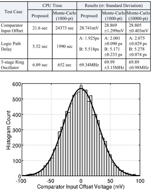
VI. BENCHMARK RESULTS
Table II summarizes the benchmark results of the proposed sensitivity-based mismatch analysis via pseudo-noise simulation compared with 1,000-point and 10,000-point Monte-Carlo analysis results. The proposed mismatch analysis is significantly faster with excellent accuracy, especially for the clocked comparator example in which case the circuit had to be simulated for a long time before the offset voltage VOS settles to a final value. Fig. 9 compares the histogram of the comparator input offset voltage obtained from the Monte-Carlo analysis
and the PDF estimated by the sensitivity-based analysis. With a 1000-point Monte-Carlo simulation, the 95%-confidence interval is ±4.5% of the measured variation. With a 10,000-point simulation, the confidence interval is ±1.4%.
The simulations were run with SpectreRF on a 3.6-GHz Intel Xeon processor machine with 4GB of memory. The process technology assumed was 0.13-m CMOS with AVT=6.5mV·m and A/=3.25%·m (3-variation in IDS is approximately14% for 8.32m/0.13m nMOS device with VGS=1.0V).
VII. MISMATCH SENSITIVITY ANALYSIS FOR YIELD
OPTIMIZATION
To optimize a circuit for the highest yield or for the minimum uncertainty in performance, one needs to know the impact of each design parameter on the performance variation. Similar to the correlations, this impact factor or mismatch sensitivity can be derived from the breakdown list of mismatch contributions without any additional simulations. This is a significant advantage compared to the Monte-Carlo analysis.
The mismatch sensitivity of each design parameter can be derived based on the chain rule. For example, a transistor width
W is related to the mismatches in VT and by (4) and (5) listed in Section III.B, and the sensitivities of VT and variations with respect to W are:
(VT2)/W AVT2/(W2L)VT2/W , (14) (2/2) W A2 (W2L)(2/2) W. (15)
Therefore, if the pseudo-noise simulation reports that the variation in the performance P due to VT-mismatch is P,VT 2 and the variation due to -mismatch is P,2, then the sensitivity of the performance variation (P2) with respect to the width of that transistor W is:
P2/W = P,VT2/WP,2/W. (16)
Fig. 10 lists the sensitivities of the input offset voltage to the widths of the transistors in a variant of the StrongARM comparator [19]. As expected, the input transistor sizes
TABLEII
[image:9.612.51.299.382.691.2]SUMMARY OF BENCHMARK RESULTS.
Fig. 9. Comparison of the histogram from a 10,000-point Monte-Carlo simulation and the PDF from the pseudo-noise based mismatch analysis for the clocked comparator input offset voltage variation. The 3-variation of the
[image:9.612.313.563.587.710.2](M2-M3) have the highest impact on the input offset and they should be increased to reduce the input offset variation. In practical applications, other performance requirements such as the input loading and sampling bandwidth may pose the upper limits on these sizes.
VIII. LIMITATIONS
The noise-based mismatch analysis described in this paper relies on the linear perturbation model in (2). While this approach offers several advantages that enable quick estimation of performance variations as well as their correlations and sensitivities to design parameters, it also has a few limitations that the designers must be aware of.
One limitation is that the assumed linear perturbation model is valid only for sufficiently small mismatches. As the
mismatch in modern devices becomes more severe, it is expected that the estimates on the performance variations using the proposed pseudo-noise analysis become less accurate. Another consequence of the nonlinear circuit response and large mismatch is that the resulting performance variation may no longer be approximated as Gaussian distribution even if the mismatch parameters are normally distributed.
[image:10.612.59.286.274.438.2]Fig. 11 plots the errors in estimating the frequency variation in the ring oscillator example in Section IV-C as the transistor current mismatch is increased. It shows that due to the nonlinearity of the circuit response, the difference between the estimated variations using the proposed pseudo-noise analysis and the 1,000-point Monte-Carlo analysis reaches above 10% when the 3-variation of the current mismatch exceeds 39%. Fig. 11 also plots the normalized skewness of the frequency distribution estimated via the Monte-Carlo analysis, which we defined as 1/3/ where is the mean and is the third moment of the distribution, i.e. E[(X-)3]. The skewness indicates how asymmetric the distribution is and therefore how different it is from a symmetric, Gaussian distribution. As expected, the skewness grows with the transistor current mismatch and the frequency of the ring oscillator takes an increasingly non-Gaussian distribution. Fig. 12 shows the histogram of the oscillator frequency when the 3-variation of the current mismatch is at 44% (three times the variation in this technology). The linear, pseudo-noise analysis underestimates the standard deviation by 15.9% and the negative normalized skewness of -0.057 indicates that the distribution is slightly tilted towards the left.
Due to the fact that the described pseudo-noise analysis computes only the variance or standard deviation of the performance, it has to assume that the mismatch parameters are normally distributed if the shape of the performance distribution needs to be derived, which is bound to be a Gaussian because of the assumed linear perturbation model. Note that the proposed analysis can still estimate the standard deviation of the resulting performance accurately even if the mismatch parameters are not Gaussian-distributed, as long as
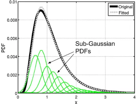
[image:10.612.65.286.510.681.2]Fig. 13. Representation of a non-Gaussian distribution as a mixture of Gaussian distributions.
[image:10.612.326.546.535.703.2]Fig. 11. Errors in estimating the standard deviation and skewness of the performance distribution versus the amount of mismatch for the ring oscillator example in Section IV-C. The error in the frequency variation reaches 10% as the 3-variation in the transistor drain current (IDS) exceeds 39%.
Fig. 12. Comparison of the histogram from a 1000-point Monte-Carlo simulation and the PDF from the pseudo-noise based mismatch analysis for the variation in the 5-stage ring oscillator frequency. The assumed 3-variation of the drain current (IDS) was 44%.
their variations are sufficiently small to keep the linear perturbation model valid. However, the proposed analysis based on linear sensitivities fails to predict the exact shape of the performance distribution when the mismatches becomes too severe or when they are not normally distributed.
While projecting non-Gaussian distributions via the nonlinear response surface is possible, it may have to sacrifice some of the strong merits of the proposed analysis such as the abilities to quickly estimate the correlations and sensitivities as discussed in Section V and VII. For example, one possible solution is to break a non-Gaussian mismatch distribution into a sum of narrowly-distributed Gaussians as illustrated in Fig. 13 and to project each of the sub-Gaussians to the performance space via its own, local linear perturbation model. The resulting performance distribution is a sum of the projected Gaussian distributions, which can be non-Gaussian. Since now the linear perturbation models must be computed individually for each center point of the sub-Gaussian PDFs, the total number of PSS simulations required increases with the number of the sub-Gaussian distributions. Unfortunately, this number can grow very quickly with the number of mismatch parameters; at a certain point, it may be more efficient to use other methods based on nonlinear response surface models (for example, [27]).
The aforementioned issues are clearly the limitations for predicting the accurate yields in the presence of severe, non-Gaussian mismatches. Nonetheless, the described pseudo-noise analysis is still very effective in quickly estimating the performance variation during design iterations and in guiding designers for possible improvements with the sensitivity and correlation information. In addition, since the accuracy achievable with 100- and 1000-point Monte Carlo simulations is limited to only ±14% and ±4.5%, respectively (the 95% confidence interval assuming Gaussian distribution), the proposed pseudo-noise analysis is a powerful tool especially for large-scale circuits which require long transient simulations and for which even moderate Monte-Carlo simulations are very costly.
IX. CONCLUSIONS
This paper presented an efficient, sensitivity-based mismatch analysis method that is based on the pseudo-noise models and LPTV noise simulation. Device mismatch is modeled as low-frequency pseudo-noise and the variation in performance is derived from the simulated LPTV noise responses. The described mismatch analysis is the most efficient extension of the DC sensitivity-based mismatch analysis [8],[9] for analyzing the mismatch effects on transient characteristics such as delay and frequency variations. In addition, it can measure correlations and determine the sensitivity of the performance variation with respect to each design parameter, all of which at no additional simulation cost. With the demonstrated speed improvement of 100-1000 over the 1000-point Monte-Carlo analysis, the variability analysis and yield optimization
problems become tractable even with the existing circuit optimization tools.
REFERENCES
[1] H. Masuda, et al., “Challenge: Variability Characterization and Modeling for 65- to 90-nm Processes,” in Proc. IEEE Custom Integrated Circuits Conf., pp. 593-600, 2005.
[2] P. Kinget, M. Steyaert, “Impact of Transistor Mismatch on the Speed-Accuracy-Power Tradeoff of Analog CMOS Circuits,” in Proc. IEEE Custom Integrated Circuits Conf., pp. 333-336, 1996.
[3] M. Orshansky, et al., “Impact of Systematic Spatial Intra-Chip Gate Length Variability on Performance of High-Speed Digital Circuits,” in Proc. IEEE/ACM Int’l Conf. on Computer Aided Design, pp. 62-67, Nov. 2000.
[4] R. K. Brayton, et al., “A Survey of Optimization Techniques for Integrated-Circuit Design,” Proc. of the IEEE, pp. 1334-1362, Oct. 1981. [5] G. Gielen and R. Rutenbar, “Computer-Aided Design of Analog and
Mixed-Signal Integrated Circuits,” Proc. of the IEEE, pp. 1825-1852, Dec. 2000.
[6] J. Kim, et al., “Fast, Non-Monte-Carlo Estimation of Transient Performance Variation Due to Device Mismatch,” in Proc. ACM/IEEE Design Automation Conf., pp. 440-443, June 2007.
[7] F. Schenkel, et al., “A Fast Method for Identifying Matching-Relevant Transistor Pairs,” in Proc. IEEE Custom Integrated Circuits Conf., pp. 361-364, 2001.
[8] J. Oehm, K. Schumacher, “Quality Assurance and Upgrade of Analog Characteristics by Fast Mismatch Analysis Option in Network Analysis Environment,” IEEE J. Solid-State Circuits, pp. 865-871, July 1993. [9] Cadence Design Systems, Inc., Virtuoso Spectre Circuit Simulator User
Guide, Product Version 5.1.41, June 2004.
[10] D. E. Hocevar, et al., “Parametric Yield Optimization for MOS Circuit Blocks,” IEEE Trans. on Computer-Aided Design, pp. 645-658, June 1988.
[11] M. J. M. Pelgrom, et al., “Matching Properties of MOS Transistors,” IEEE J. Solid-State Circuits, pp. 1433-1439, Oct. 1989.
[12] K. S. Kundert, “Introduction to RF Simulation and Its Application,” J. Solid-State Circuits, pp. 1298-1319, Sept. 1999.
[13] M. Okumura, et al., “Numerical Noise Analysis for Nonlinear Circuits with a Periodic Large Signal Excitation Including Cyclostationary Noise Sources,” IEEE Trans. on Circuits and Systems-I, pp. 581-590, Sept. 1993.
[14] J. Roychowdhury, et al., “Cyclostationary Noise Analysis of Large RF Circuits with Multitone Excitations,” IEEE J. Solid-State Circuits, pp. 324-336, Mar. 1998.
[15] A. Demir, et al., “Phase Noise in Oscillators: A Unifying Theory and Numerical Methods for Characterization,” IEEE Trans. on Circuits and Systems-I, pp. 655-674, May 2000.
[16] R. Telichevesky, et al., “Efficient Steady-State Analysis based on Matrix-Free Krylov-Subspace Methods,” in Proc. ACM/IEEE Design Automation Conf., pp. 480-484, June 1995.
[17] R. Telichevesky, et al., “Efficient AC and Noise Analysis of Two-Tone RF Circuits,” in Proc. ACM/IEEE Design Automation Conf., pp. 292-297, June 1996.
[18] A. Demir, et al., “Time-Domain Non-Monte Carlo Noise Simulation for Nonlinear Dynamic Circuits with Arbitrary Excitations,” IEEE Trans. on Computer-Aided Design, pp. 493-505, May 1996.
[19] J. Montanaro and et al., “A 160MHz, 32b, 0.5W CMOS RISC Microprocessor,” IEEE J. Solid-State Circuits, pp. 1703-1714, Nov. 1996.
[20] L. W. Nagel, "SPICE2: A Computer Program to Simulate Semiconductor Circuits," Berkeley, CA: Univ. of California, Ph.D. dissertation, May 1975.
[21] W. A. Gardner, Introduction to Random Processes with Applications to Signals and Systems, 2nd Edition, New York: McGraw Hill, 1989. [22] J. Roychowdhury, “Theory and Algorithms for RF Sensitivity
Computation,” IEEE Int’l Symp. on Circuits and Systems, pp. V-225-V-228, May 2002.
[24] C. Galup-Montoro, et al., “A Compact Model of MOSFET Mismatch for Circuit Design,” IEEE J. Solid-State Circuits, pp. 1649-1657, Aug. 2005. [25] S. W. Director and R. A. Rohrer, “The Generalized Adjoint Network and Network Sensitivities,” IEEE Trans. on Circuit Theory, pp. 318-323, Aug. 1969.
[26] U. Choudhury, “Sensitivity Computation in SPICE3,” M.S. Thesis, EECS Dept., Univ. Calif. Berkeley, Elec. Res. Lab., Dec. 1988.
[27] X. Li, et al., “Asymptotic Probability Extraction for Non-normal Performance Distributions,” IEEE Trans. on Computer-Aided Design of Integrated Circuits and Systems, pp. 16-37, Jan. 2007.
[28] T. Serrano-Gotarredona and B. Linares-Barranco, “A New Five-Parameter MOS Transistor Mismatch Model,” IEEE Electron Device Letters, pp. 37-39, Jan. 2000.