Analysis and Design of a Modular Multilevel
Converter With Trapezoidal Modulation
for Medium and High Voltage DC-DC Transformers
I. A. Gowaid, Student Member, IEEE, Grain P. Adam, Member, IEEE, Shehab Ahmed, Senior Member, IEEE,
Derrick Holliday, and Barry W. Williams
Abstract—Conventional dual-active bridge topologies provide
galvanic isolation and soft-switching over a reasonable operating range without dedicated resonant circuits. However, scaling the two-level dual-active bridge to higher dc voltage levels is impeded by several challenges among which the high dv/dt stress on the cou-pling transformer insulation. Gating and thermal characteristics of series switch arrays add to the limitations. To avoid the use of standard bulky modular multilevel bridges, this paper analyzes an alternative modulation technique, where staircase approximated trapezoidal voltage waveforms are produced; thus, alleviating de-veloped dv/dt stresses. Modular design is realized by the utilization of half-bridge chopper cells. This way the analyzed dc-dc trans-former employs modular multilevel converters operated in a new mode with minimal common-mode arm currents, as well as re-duced capacitor size, hence rere-duced cell footprint. Suitable switch-ing patterns are developed and various design and operation as-pects are studied. Soft-switching characteristics will be shown to be comparable to those of the two-level dual-active bridge. Experi-mental results from a scaled test rig validate the presented concept.
Index Terms—DC fault, dc/dc power conversion, dc transformer,
dual-active bridge, modular multilevel converter (MMC).
NOMENCLATURE
Tt Voltage transit time between the two dc rails.
N Number of cells per arm (or series IGBTs per valve).
Ns Number of ac voltage steps.
Td Dwell time spent in each voltage level.
Vdc DC-link voltage. m Modulation index.
fs, ωs Fundamental frequency (fs = 1/Ts).
td(off ) IGBT turn-off delay time. tf IGBT fall time.
Manuscript received May 20, 2014; revised July 27, 2014 and October 15, 2014; accepted November 17, 2014. Date of publication December 5, 2014; date of current version May 22, 2015. This work was supported by the EPSRC Na-tional Centre for Power Electronics under Grant EP/K035304/1. Recommended for publication by Associate Editor M. A. Perez.
I. A. Gowaid is with the Department of Electronic and Electrical Engineering, University of Strathclyde, G1 1XW Glasgow, U.K., and also with the Electri-cal Engineering Department, Faculty of Engineering, Alexandria University, Alexandria 21544, Egypt (e-mail: [email protected]).
G. P. Adam, D. Holliday, and B. W. Williams are with the Depart-ment of Electronic and Electrical Engineering, University of Strathclyde, G1 1XW Glasgow, U.K. (e-mail: [email protected]; derrick.holliday@ strath.ac.uk; [email protected]).
S. Ahmed is with the Texas A&M University at Qatar, Doha, Qatar (e-mail: [email protected]).
Color versions of one or more of the figures in this paper are available online at http://ieeexplore.ieee.org.
Digital Object Identifier 10.1109/TPEL.2014.2377719
td(on) IGBT turn-on delay time. tr IGBT rise time.
tD B Dead time (underlap time) between two IGBTs. Z∗ Set of nonnegative integers.
Z+ Set of positive integers.
I. INTRODUCTION
D
C grids of various topologies, structures, and voltage lev-els are drawing increasing attention, a tendency driven by the rapidly advancing power electronics technology and the un-precedented growth of global energy demand. Migration from ac to dc systems is further promoted by the steadily rising de-pendence on renewable distributed generation, the economic challenges of long-distance bulk power transmission, and the nature of available energy storage technology. As high-voltage dc (HVDC) proves economical for, for instance, transporting large-scale wind power generated offshore, utilization of dc col-lector grids may spare the extra conversion stages needed when wind plants use ac collection networks. Moreover, most of en-ergy storage devices considered for industrial, transportation, and power system applications are typically interfaced either by dc connections or through a dc conversion stage [2].In power systems, the evolution of dc grids awaits a technical leap in dc protection and an efficient means of dc voltage level transformation [3]. For a high-power dc–dc converter to compete with the high efficiency standards set by ac power transformers, hard switching is not a viable option. Soft-switching, on the other hand, has long been investigated and can be achieved by, for instance, resonant converters [4]–[8]. However, significant challenges impede the scaling of most resonant designs to the high-power high-voltage range. That is, resonant stages experi-ence high internal voltage stresses and, hexperi-ence, require a special insulation design. Additionally, in practice inductance and ca-pacitance values drift owing to aging and operating conditions. In transformerless resonant designs, lack of galvanic isolation may be an additional drawback [9], [10].
Dual active bridge (DAB) dc–dc converters, first proposed in [11] for an industrial application, classically employ two H-bridges or three-phase bridges connected via an ac trans-former, in what can be termed a front-to-front connection [12]– [18]. Bidirectional power flow is possible and is controlled by the voltage across the transformer leakage inductance [13]. Typ-ically, power flow direction and magnitude are dictated by the phase shift angle between the bridges, as well as their individ-ual voltage output magnitudes [18]. Utilizing an ac transformer
stage offers the galvanic isolation necessary for servicing, reliability, and grounding. Zero-voltage switching of both bridges is assured within a certain operating range, subject to the internal structure of each bridge [15]. DAB converters have been considered for solid-state ac transformers, which are ex-pected to play a key role in a wide spectrum of applications including dc distribution [3].
On the downside, traditional DAB converters typically oper-ate at a high-switching frequency in order to reduce ac trans-former volume. This is not viable for higher power and voltage levels due to thermal and gating limitations of high-voltage power electronic device arrays. Furthermore, the impact of ac transformer parasitic components is more pronounced with higher voltage, rendering transformer design a challenging task. Therefore, potential high-power DAB converter designs must employ reasonably low-switching frequencies [19]. Another problem is dv/dt stress [20]. In a two-level mode, a high-voltage DAB converter will produce a potentially destructive dv/dt upon transformer insulation. This stress results in insulation degrada-tion and eventually breakdown, and must be relieved to allow for voltage scalability.
One of the DAB prototypes developed for a 1-MW solid-state ac transformer was reported in [19]. The 12-kV/1200-V DAB employs a modular design in which six 2-kV/400-V DAB con-verter modules were series connected at the 12 kV side and series-parallel connected at the 1200 V side. A diode clamped topology was proposed for each 2-kV bridge. Though promis-ing, it is not clear how challenges facing higher voltage/power versions of such a topology are to be addressed, with regard to the optimum choice of voltage ratings, number of mod-ules, switching frequency, complexity of connections, number of components, and capacitor balancing issues [21].
Front-to-front connections of modular multilevel converters (MMC) or the so called alternate arm converters have been ana-lyzed in [22] in attempt to build an efficient, low dv/dt, and rel-atively compact modular dc–dc converter. A similar connection is presented in [23], where each MMC contributes to the volt-age stepping in addition to the ac transformer stvolt-age. Each MMC operates under either sinusoidal or two-level modulation, form-ing what can be termed an “electronic dc tap changer.” Bipolar MMC cells are employed in the lower voltage-side MMC to boost the voltage. When the voltage gain of the lower voltage-side converter is higher than unity, each cell must be rated at the lower voltage dc-link voltage. It is therefore suited for medium and low-voltage applications.
Direct-connected high-power dc–dc converters have been re-ported in [24], [25]. They lack galvanic isolation which may limit their application scope.
An improved design of conventional two-level bridge convert-ers has been proposed in [26] and [27] for HVDC applications. The voltage square wave slopes are reduced by introducing in-termediary voltage steps, such that the bridge output voltage resembles a trapezoidal waveform. A capacitor in series with an IGBT/antiparallel diode pair shunts every IGBT in all arms of the conventional two-level converter. The added shunt com-ponents act as active soft-voltage clamps, as well as energy tanks for brief periods. Structure wise, the converter enjoys the
same half-bridge cell-based modular structure as a conventional MMC, facilitating manufacturing, installation, and mainte-nance. The size of passive components, as well as conduction losses are lower than a typical MMC of same voltage and power ratings [26]. This paper extends the analysis presented in [26] for generic medium-/high-voltage DAB applications, focusing on bridge operation aspects. It will be shown that the opera-tion of the considered converter is distinct from a convenopera-tional MMC.
The analyzed converter is denoted as a “quasi two-level con-verter (Q2LC)” for expedience. Switching patterns, harmonic content, and voltage modulation techniques of the Q2LC are dis-cussed. Cell capacitance is quantified and the use of the Q2LC as the building block in a high-power high-voltage DAB dc–dc converter is analyzed. An insight on soft-switching capabilities is presented, and finally, experimental validation of the concept is provided.
In addition to serving as a high voltage dc-dc transformer, the proposed concept is expected to help extend the application of solid-state ac transformers to the medium and upper medium voltage ranges.
II. STRUCTURE ANDOPERATINGPRINCIPLE OF THEQ2LC
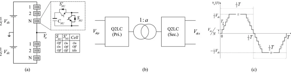
The single-leg Q2LC structure is outlined in Fig. 1(a). The bold lines represent the main power paths, traditionally, a series array of IGBTs in each bridge arm. A simple auxiliary circuit of a capacitor and an IGBT/diode pair is connected across each main path IGBT/diode pair. The added circuit provides an auxiliary path for power flow. Every time ac pole voltage polarity is reversed, an appropriate switching pattern permits the auxiliary circuit of each main IGBT to act as an energy buffer, where the load current flows through the capacitor, whose voltage acts upon the load. Simultaneously, the auxiliary circuit acts as a switched soft voltage clamp, resulting in equal dynamic and static voltage sharing between all the main IGBTs of an arm. The insertion of auxiliary shunting capacitors allows for sequential switching of the main IGBTs in each arm in brief time steps Td
(order of microseconds) summing to a total transition timeTt, where
Tt = (N−1)Td. (1)
Td is the dwell time spent at each intermediary voltage level during ac pole level transitions. Being a few microseconds, choice of the dwell time must account for the on and turn-off times of the IGBT modules and ensure an acceptable level of dv/dt stress. On the other hand, a largeTt implies higher energy buffering requirements; hence, relatively larger auxiliary capacitances.
Fig. 1. (a) Single-leg Q2LC, (b) Generic structure of a Q2LC-based DAB, and (c) the output voltage waveform of the single-leg Q2LC.
controllers must ensure balanced capacitor voltages within an acceptable band around this set point.
A two-level converter where the main IGBTs are shunted by the said auxiliary circuits evolves to an MMC structure [26]–[37], where the trapezoidal modulation technique allows for reduced passive component values. Typical half-bridge chopper cell design can be utilized, with all the advantages of a modular structure.
With stepped voltage transitions introduced between −1/2Vdc and 1/2Vdc, the steady-state voltage seen by each
arm in Fig. 1(a) is
vX =Vdc(1−NYon/N) (2)
where subscriptsX ∈ {U, L} andY = ¯X. Symbols U and L refer to the upper and lower arms, respectively. In (2), NYon
is the number of inserted auxiliary capacitors in the com-plementary arm. The ac pole is tied to one of the dc rails whenNYon∈ {0, N}. Stepped voltage transitions occur when
1 ≤NYon < N, in a staircase approximation of a trapezoid.
Since the voltage across both arms of a pole at any instant equals the dc-link voltage, maintaining the capacitors voltages around theVdc/N set point requires that the total number of
inserted auxiliary capacitors in both arms at any instant satisfies (3), entailing a complementary switching (CS) patterns of both arms of the same phase leg [29],[30]
NUon+NLon=N. (3)
However, the Q2LC operating mode permits the use of a third switching state—denoted idle state—where both the main and auxiliary IGBTs are in an off-state[see Fig. 1(a)]. Possible switching patterns employing this switching state, as will be shown in Section II-A, are able to achieve proper operation withNUon+NLon< N. The single-leg Q2LC output voltage
expression is given in (4). Equation (4) holds for all switching patterns. Nonetheless, when the idle state is employed, the arm having idle cells is to be avoided while applying (4).
vo(t) =Vdc
1 2 −
NUon(t) N
=Vdc
NLon(t)
N −
1 2
. (4)
In production of the quasi-two-level ac output, the Q2LC is not required to produce an N+ 1 voltage levels when N low-voltage cells are installed per arm. The main Q2LC design constraint can be set to the selection of voltage level counts,Td,
andωs values to alleviate the dv/dt stress at minimum drop in fundamental voltage magnitude and with minimum cell capaci-tance. This issue will be revisited several times along this paper. In order to achieve such a compromise especially at higher dc voltages, the number of output ac voltage levels may need to be reduced fromN+ 1toNs+ 1, where
Ns =N/n (5)
and n is the number of cells per cell subgroup. The minimum value ofNs, which corresponds to the upper value of n, is subject to the permissible dv/dt levels. In such a case, each subgroup will be composed of n MMC half-bridge cells effectively series connected, where equal static and dynamic voltage sharing is assured by the auxiliary capacitors. Gating delays may cause slight voltage imbalance between capacitors of the subgroup. To avoid complex gate drive/snubbering circuitry, the employed capacitor balancing technique will need to address individual cell capacitors of the arm rather than cell subgroups.
As an alternative to cell grouping, medium voltage half-bridge cells can be employed, where IGBT/diode modules are series connected to form the main and auxiliary cell switches, as in the cascaded two-level converter [38]. In this case, N becomes the total number of main path IGBTs per arm and n denotes the number of series IGBT/diode pairs per cell.
In either approach, a suitable redundancy margin in terms of cell numbers/ratings is mandatory for uninterrupted and bal-anced operation of the Q2LC with faulted cells.
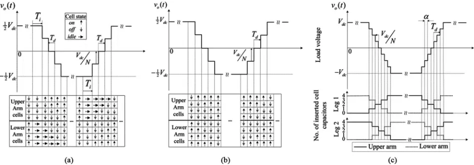
A. Switching Sequences
Four possible switching patterns can be employed to achieve stepped two-level operation, and are termed “noncomplemen-tary switching (NCS),” “CS,” “shifted complemen“noncomplemen-tary switching (SCS),” and “shifted noncomplementary switching (SNCS),” modes.
1) Noncomplementary Switching: In this pattern, all three
possible switch states of each cell[see Fig. 1(a)]are exploited. The switching sequence is shown in Fig. 2(a) for a four cell-per-arm, single-leg Q2LC. Starting with the load voltage at1/2Vdc,
Fig. 2. Q2LC cell states with different switching sequences. (a) NCS sequence, (b) CS sequence, and (c) SCS sequence.
voltage variations occurring while the ac pole is clamped to ei-ther of the dc rails. For a stepped voltage transition from1/2Vdc
to−1/2Vdc to occur, capacitorsC1U toC4U are sequentially inserted by switching-on the corresponding cells with a dwell delayTd. The load voltage transits to−1/2Vdc in four discrete
steps, each being1/4Vdc. During the transition, the lower arm
voltage decreases in1/4Vdc steps, according to (2). For each
step voltage drop, a lower arm cell is switched-off. With the last upper arm capacitor inserted into the circuit, the last lower arm cell turns off, and the pole load current commutates from the upper arm to the lower arm. A few microseconds (Ti) be-fore the next load voltage polarity reversal, the upper arm cells are switched to an idle state, and a similar switching procedure is repeated for the voltage transit from −1/2Vdc to 1/2Vdc,
as in Fig. 2(a). The idle cells of an arm could alternatively be switched-off simultaneously at the instant when the last capac-itor of the complementary arm is inserted. However, this may bring about additional switching losses, depending on the load-ing conditions at the instant of switchload-ing.
2) Complementary Switching: In this switching sequence
[see Fig. 2(b)], cells are utilized only in the ON or OFF states (no idle state). Cells of both arms switch in a complementary pattern. WithNLon =N−NUon, the number of inserted
ca-pacitors in one arm always equals the number of off-state cells in the other arm of the same leg. This is a similar principle to conventional MMC switching [31]–[33]. Equation (3) holds for this switching mode. Therefore, according to (2) and (3), arm voltages are continuously complementary over the fundamental cycle.
3) Shifted Complementary Switching: The use of this
switch-ing pattern is preferred for sswitch-ingle-phase H-bridge Q2LCs. The SCS sequence produces 2Ns+ 1 levels in the output voltage by introducing a time lag0< α < Td between the switching functions of the two phase legs, where the arms in each leg switch complementarily as in the CS sequence. This is shown in Fig. 2(c). The SCS sequence produces a further relieved dv/dt stress for the same value of Tt. A Q2LC of N cells per arm operating with the SCS sequence is functionally equivalent to
a Q2LC structure of 2N cells per arm operating with the SC sequence and a smaller dwell time (1/2Td whenα= 1/2Td), therefore has similar voltage and current dynamics as featured with the CS sequence.
The delayαcan alternatively be inserted between the com-plementary switching functions of both arms of the same leg; thus, becoming valid for single-leg and three-phase Q2LCs as well. However, this may trigger extra common-mode currents. This applies to SNCS as well. A further study is needed.
4) Shifted Noncomplementary Switching: Similarly, a SNCS
sequence can be produced by inserting a delay 0< α < Td between the switching functions of the two phase legs of a single-phase H-bridge Q2LC, where the arms in each leg switch in a noncomplementary manner as in the NCS sequence. Again, operation is functionally equivalent to Q2LC with double the number of cells per arm operating under the NCS sequence with a smaller dwell time; thus, with alleviated dv/dt stress.
The analysis carried out in the rest of this paper will consider the CS and NCS sequences for the study of various operation aspects of Q2LCs. However, all conclusions are valid for oper-ation with SCS and SNCS sequences—after accounting for the doubled number of levels and shorterTd—as duals to CS and NCS, respectively, unless otherwise stated.
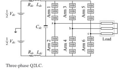
B. Q2LC Operation
Fig. 3. Three-phase Q2LC.
TABLE I
PARAMETERS OF THECONSIDEREDTHREE-PHASEQ2LC
Vd c ±30 kV fs 250 Hz
LL(phase) 1.5 mH Ld c 1 mH
RL(phase) 40Ω Rd c 0.1Ω
Td 5μs Cd c 100μF Cs m 80μF Ra r m 80 mΩ
Ns 10 La r m 16.5μH
operation with 1.8 kV per cell, or 2 kV per cell with three cells per arm bypassed (e.g., failure). The IGBT on-state and diode forward voltages are modeled as per the datasheet. A 0.5-μH stray inductance is modeled for each half-bridge cell. The cells of each arm are arranged in subgroups to produce
Ns= 10with 80-uF capacitance per subgroup. Individual cell voltages are balanced using the conventional sorting algorithm used for MMCs, where cell capacitors are continuously rotated based on measurements of their individual voltages and arm current polarities [34]–[36].
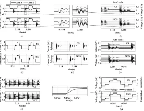
Fig. 4 depicts the output voltage, output current, arm cur-rents, and cell voltages for both CS and NCS sequences. With a modulation indexmf = 1, the output voltage exhibits stepped behavior with a total of eleven (Ns+ 1) voltage levels indepen-dent of the switching sequence[see Fig. 4(g)]. Except during switching periods, only one arm per leg conducts the full load current, similar to a conventional two-level bridge. When ac pole voltage transition is realized by the CS sequence, load current flows simultaneously in both arms and nearly all cell capaci-tors in the leg experience current flow. With the connected load being inductive, this current will be charging for the capacitors of the switching-off arm (in which cells switch successively to the on-state) and discharging for the switching-on arm, where cells switch to the off state. The net result is that cell capacitors in each arm charge or discharge some of their energy once per half cycle of the fundamental frequency with voltage variation confined to a certain ripple band by action of the capacitor bal-ancing technique. Fig. 4(b) and (e) shows that the ripple is about ±1.6% the nominal cell subgroup voltage.
Any ripple in the dc-side voltage will be exported (pro rata) to the on-state cells in each leg, since they must instantaneously balance with the dc-side voltage. This is the reason for the slight voltage variation observed in the on-state cells while load current fully flows in the complementary arm [see Fig. 4(b) and (e)]. A common-mode current is triggered in each leg dur-ing switchdur-ing periods. This current, actdur-ing to regain voltage
balance between each leg and the dc link, is limited by stray circuit impedance. As modeled, the individual cell stray arm inductances sum up to 16.5μH per arm, while the equivalent device on-state resistance per arm is about 80 mΩ. Resonance between connected leg capacitance and the parasitic inductance triggers common-mode oscillations as seen in Fig. 4(a). It is ob-served that these oscillations are of insignificant magnitude and damp rapidly without dedicated arm resistance. These Q2LC internal current and voltage dynamics are not reflected on to the load side, as confirmed in Fig. 4(g).
The Q2LC exhibits slightly different internal voltage and cur-rent dynamics when the NCS sequence is employed. Nonethe-less, the load side remains isolated from these dynamics as well. Each capacitor remains in conduction path for an aver-age period of 1/2Ts−Ti, where its voltage follows any dc-link ripple pro rata and, then, becomes bypassed for the rest of the fundamental period. Unlike the CS sequence, the full-load current flows through cell capacitors of the switching-off arm brought into the conduction path. In consequence, the cell sub-group voltage ripple becomes±2% peak-to-peak for the same 80-μF cell subgroup capacitance. At the instant the last cell of the switching-on arm switches from idle to off, cell capacitors of the switching-off arm are all in conduction path and instan-taneously balance with the dc-link voltage, triggering common-mode currents with slightly higher peak and oscillations as compared to CS sequence[see Fig. 4(a)]. It will be shown in section IV that NCS (SNCS) may offer better switching charac-teristics.
It can be seen in Fig. 4(d) that the current flow in the auxiliary circuit is significantly less than in the main path IGBT modules, apart from the adopted switching sequence. This allows the use of lower current rating devices in the auxiliary circuit. Further-more, it extends the life time of cell capacitors. In this test the FZ400R33KL2C IGBT module from Infineon with 3300 V 400 A are used for the auxiliary circuit in each cell. Note that the peak auxiliary circuit “pulse” current depends on the instant the cell balancing controller brings the capacitor into conduction path. It is worth noting as well that the cell balancing controller succeeds to sustain such a low-voltage ripple while modeled to measure cell voltages only twice per half cycle. Neverthe-less, cell voltages may need to be frequently polled for failure handling.
III. Q2LC COMPONENTSIZING
In a Q2LC-based dc/dc converter for dc-grid applications, capacitors briefly engage in power transfer with a small power factor range relative to an ac/dc conversion application, which facilitates capacitor size estimation. Investigation of current flow through the ac stage of the Q2LC-based DAB converter is mandatory for capacitance calculation.
Fig. 4. Simulation results for the Q2LC of Fig. 3 and Table I. (a) Arm currents, (b) arm 3 cell voltages (six cells), (c) main path IGBT/diode current, (d) auxiliary IGBT/diode current, (e) arm 4 cell voltages (four cells), (f) time window of balanced arm four cell voltages, and (g) phase b output voltage and current.
inductanceLs. The ac transformer series resistance is neglected. Auxiliary capacitance size in a Q2LC cell is subject to the ac pole current profile during the switching period Tt. The cell subgroup capacitance of the primary and secondary sides (Cgp
andCgs, respectively) can be expressed as
Cgp = γ Ns
ωsVdcp
ωsTt+θo
θo
i(θo) + 1
ωsLs
θ
θo
vLs(θ−θo)dθ
dθ
Cgp = ρ2a2Cgs (6)
where i(θ) is the ac pole current andγis a factor of safety to account for the impact of Q2LC common-mode arm currents and the neglected series resistance (γ≥1).is the capacitor voltage ripple in per unit (e.g.,= 0.1 for 10% peak-to-peak capacitor voltage ripple). The dc ratio isρ=b/a, where a is the ac transformer turns ratio andVdcs =bVdcp. Voltage transition
periods are assumed equal for both bridges (Ttp =Tts =Tt).
Equation (6) is set to design the first subgroup capacitance of the switching-off arm to be brought into conduction path. Under inductive loading and NCS, this capacitor sustains full load current flow for a time Tt and undergoes the highest voltage variation. All cell subgroup capacitances need to be sized to this value since they circulate to the top rank of the switching sequence.
Starting at point 0 in Fig. 5(b), whereθ= 0, the formulae for vL s(θ)for each section of a half cycle can be developed and the primary phase currentip(θ)can be calculated in terms of its initial value ip(θo), where θo = 0. Using the property
ip(0) =−ip(π),ip(0)and all half-cycle currents are calculated as given in the Appendix. From which all three-phase currents can be constructed. It is noteworthy that during the voltage tran-sition periodTtof each phase leg in either bridge, the respective ac pole current is parabolic. The calculations carried out in this section and in the Appendix are valid for the range of load angles
Fig. 5. (a) Block diagram of a generic three-phase Q2LC based DAB con-verter, and (b) ac voltages and currents of one transformer phase referred to the primary side[isis the secondary-side phase current referred to primary].
profiles of segment CD, where13π+ϕ≤θ≤ 31π+ϕ+ωsTt, and segment EF, where 23π≤θ≤23π+ωsTt, are important for switch rating selection. The current flow during Tt for
ϕ≤θ≤ϕ+ωsTt(segment AB) andπ≤θ≤π+ωsTt (seg-ment GH) are of particular importance for cell capacitor sizing. Switching devices are to be rated at the peak arm current, which is the peak phase current, at rated power conditions. The peak of phase current at rated power flow (i.e.,ϕ=ϕm ax) is subject
to the dc ratio. In dc-grid applications, the dc ratio in a DAB can vary within a limited range around unity depending on loading and by action of converter controllers. Atϕ=ϕm ax, the local
phase current peak value within segment CD is the maximum phase current magnitude whenρ=ρm ax, ρm ax >1and occurs
atvL s(θC D) = 0. Whenρ=ρm in,ρm in<1, the phase current
maximum magnitude (atϕ=ϕm ax) shifts to segment EF
oc-curring atvL s(θEF) = 0. Using the Appendix, the maximum
current valuesipk
p (θ
pk
C D),ipkp (θ
pk
EF), and the corresponding
an-glesθpkC DandθEFpk are obtained as in (7) forρm ax ≥1and as in
(8) forρm in ≤1
θC Dpk = 1
ρωsTt(2−ρm ax) +ϕm ax +
1
3π (7a)
ipkp (θpkC D) = Vdcp 3ωsLs
⎛ ⎜ ⎝
ρm ax−3 +
2
ρm ax
ωsTt
+ 2ϕm ax+ (ρm ax−1) π
3
⎞ ⎟ ⎠ (7b)
θEFpk = 2(1−ρm in)ωsTt+ 2
3π (8a)
ipkp (θpkEF) = Vdcp 3ωsLs
⎛ ⎝(2ρ
2
m in−3ρm in+ 1)ωsTt
+ 2ρm inϕm ax+ (1−ρm in) π
3
⎞ ⎠. (8b)
In case a DAB design requiresρm in >1, then (7) defines the
phase current maximum value. Similarly, ifρm ax <1, then (8)
defines the phase current maximum magnitude. Equation (7) is also valid for partial loading for any ρ >1 and ωsTt ≤ϕ≤
1
3π−ωsTt, whereas (8) is valid for partial loading as long as ρ <1 andωsTt ≤ϕ≤13π−ωsTt. Atρm in =ρm ax = 1, the
peak currents in (7) and (8) will reduce to
ipkp (θ) = 2Vdcpϕm ax 3ωsLs
. (9)
When rating switching devices current capacity, the higher of the current values produced by (7) and (8) is considered. A factor of safety may be introduced. Equations (7)–(9) represent currents of the primary side. The maximum current of the sec-ondary sideipk
s (θ)can be described by (7)–(9) divided by the factorρa.
In segments AB and GH, the formulae ofvL s(θ)andip(θ) are given in (10)–(13). Forϕ≤θ≤ϕ+ωsTt
vLs(θA B) = Vdcp
3
(ρ+ 1)− 2ρ
ωsTt
(θ−ϕ)
(10)
ip(θA B) = Vdcp 3ωsLs
⎛ ⎝−
ρ ωsTt
(θ−ϕ)2+ (ρ+ 1)
×(θ−1
2ωsTt) + 2(ρ−1)
π
3 −ρϕ
⎞ ⎠. (11)
Forπ≤θ≤π+ωsTt
vLs(θG H) = Vdcp
3
(1−ρ)− 2
ωsTt (θ−π)
(12)
ip(θG H) = Vdcp 3ωsLs
⎛ ⎜ ⎜ ⎝
− 1
ωsTt
(θ−π)2+ (1−ρ)
×(θ−π
3 − 1
2ωsTt) +ρϕ
⎞ ⎟ ⎟
⎠. (13)
The phase current has no dc offset and, consequently,ip(θ) = −ip(θ+π). Also, current polarity is irrelevant for capacitor sizing; therefore, the currents of (11) and (13) at rated conditions are sufficient to quantify the maximum arm current flow during switching periods over the fundamental cycle.
Forϕ >0,ip(θA B)is higher thanip(θG H)forρ >1and is
lower than ip(θG H) for ρ <1. Equations (11) and (13)
con-firm this for ωsTt≤ϕ≤ 13π−ωsTt. Also, they show that
ip(θA) =ip(θH)andip(θB) =ip(θG)forρ= 1. At rated
con-ditions whereϕ=ϕm axand forρ=ρm ax, ρm ax >1, (6), (10),
and (11) are used to calculate the primary-side capacitance re-quirementCgpat rated power, given as
Cgp =γ NsTt 3ωsLs
ϕm ax+ 2(ρm ax−1) π
3 −
ρm ax
3 ωsTt
.
TABLE II
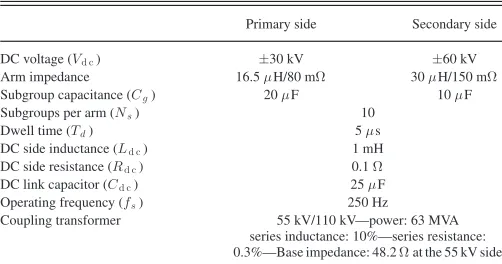
PARAMETERS OF THESIMULATEDTHREE-PHASEQ2LC-BASEDDAB
Primary side Secondary side
DC voltage (Vd c) ±30 kV ±60 kV
Arm impedance 16.5μH/80 mΩ 30μH/150 mΩ
Subgroup capacitance (Cg) 20μF 10μF
Subgroups per arm (Ns) 10
Dwell time (Td) 5μs
DC side inductance (Ld c) 1 mH DC side resistance (Rd c) 0.1Ω
DC link capacitor (Cd c) 25μF Operating frequency (fs) 250 Hz
Coupling transformer 55 kV/110 kV—power: 63 MVA series inductance: 10%—series resistance: 0.3%—Base impedance: 48.2Ωat the 55 kV side
Forρ=ρm in, ρm in <1, (6), (12), and (13) are used to
calcu-lateCgpat rated power as
Cgp=γ NsTt 3ωsLs
ρm inϕm ax+ 2(1−ρm in) π
3 − 1 3ωsTt
.
(15) Equation (14) gives the design value of Cgp when the dc
ratio ultimate valuesρm in andρm ax are both above unity.
Oth-erwise, if ρm in and ρm ax are both designed to be less than
unity, the required capacitanceCgpis given by (15). If the
sys-tem is designed such thatρm in ≤1andρm ax >1, the required
capacitance size is given by (14) when the condition in (16) is true, otherwise the capacitance is designed by (15)
ρm ax≥
4π−3ϕm ax−ωsTt+ρm in(3ϕm ax−2π)
2π−ωsTt
. (16)
Whenρm ax =ρm in= 1, (14) and (15) reduce to
Cgp=γ NsTt 3ωsLs
ϕm ax −
1 3ωsTt
. (17)
Switch rating and capacitance design carried above consid-ers bidirectional rated power flow. A similar derivation when
ϕm ax < ωsTtcan be done. Nonetheless, calculations using the given equations atϕm ax =ωsTtare expected to produce prac-tically insignificant errors. The switch rating and capacitance design methods can be acceptably simplified by using (9) and (17) with appropriate safety factors to account for dc ratio range as well as other operation aspects (see section VII).
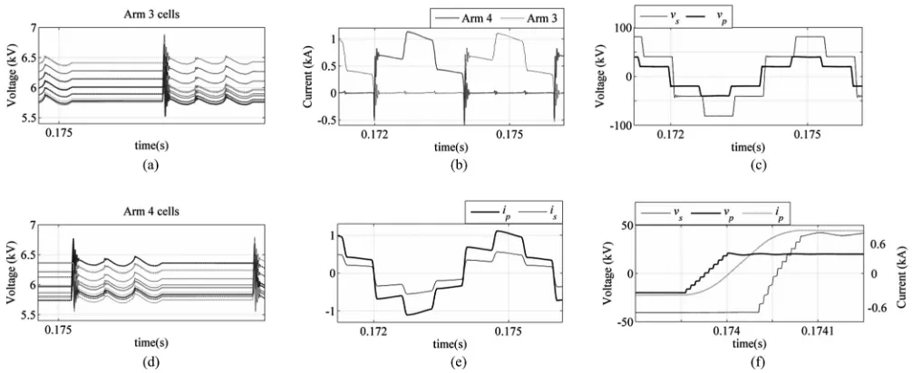
A simulation case study will be used to assess the proposed design method for device ratings and cell capacitances. The ±30-kV three-phase Q2LC described in Section II is connected to another±60-kV three-phase Q2LC through an ac transformer to form a DAB converter. The±60-kV side is considered the secondary side. Both converters are connected to stiff dc sources through impedance as per Table II. The ac transformation stage is modeled as a three-phase linear transformer with 10% leakage inductance, 0.3% series resistance, and 1:2 primary to secondary turns ratio. Each cell of the±60-kV Q2LC model employs In-fineon’s IHV FZ800R33KL2C IGBT module with 3300 V and 800 A for the main power path, and the IHV FZ400R33KL2C IGBT module with 3300 V and 400 A for the auxiliary path. The
[image:8.594.42.293.92.224.2]modeled values of IGBT on-state and diode forward voltages are taken from datasheets. A 0.5-μH stray inductance is modeled for each half-bridge cell. Sixty cells per arm are connected in se-ries for operation at 2 kV per cell for redundancy. This way, the equivalent device on-state resistance modeled per arm is 150 mΩ and the arm stray inductance is 30 μH (60 μH × 0.5 μH). Cells are grouped in subgroups with Ns= 10 (i.e., n= 6). Both Q2LCs employ NCS sequence. A load angleϕ= 7.2°is modeled such that 60 MW flows from primary to secondary. The secondary dc voltage is set to ±60.6 kV to produce a dc ratio ρ= 1.01. Other system parameters are summarized in Table II.
Fig. 6 shows results obtained mainly from the primary side with 2% dc voltage ripple. Fig. 6(f) shows thatϕ > ωsTt and
ρ >1; hence, (7) is used to calculate the peak of the primary-phase current (arm current) yielding 1080 A. This is in close agreement with the simulated value given in Fig. 6(b). Also, at the instant phase b ac pole becomes tied to the negative dc rail through arm 4, the arm current is found to reach over 800 A although (36) or (37) atθ=ϕ+ωsTt in the Appendix expect an arm current value of 605 A. This mismatch is due to the superimposed common-mode current component seen in Fig. 6(b). Note that the maximum arm currents of the primary and secondary converters are well below the selected device current ratings.
If the said power flow and load angle represent rated condi-tions (i.e.,ϕm ax = 7.2°,ρm ax =ρm in = 1.01), the previously
calculated peak phase current can be used to design device rat-ings to the values detailed above while allowing for a factor of safety. At the same rated conditions, the cell subgroup capac-itance can be designed using (14). Withγ= 1 and for±10% cell voltage ripple, (14) producesCgp = 20μF. This value
ac-counts for reverse power flow as well. As seen in Fig. 6, extra voltage ripple results from common mode current. The ripple was found to be confined to±10%in primary and secondary sides irrespective of power flow direction when Cgp = 25μF
(i.e.Y = 1.25).
When medium voltage half-bridge cells are employed like in a cascaded two-level converter (refer to Section II), the ca-pacitance Cgp represents the individual cell capacitance.
Al-ternatively, when Cgp is the aggregate capacitance of a
sub-group of cells, the cell capacitance is Ccell=nCgp. For the
current example, where n= 3, Ccell= 75 μF is required.
In the secondary side, where Cgs= 6 μF for ±10%
volt-age ripple and n= 6, Ccell is nearly 36 μF. For
compar-ison, a regular MMC in sinusoidal mode with the same number of cells per arm and power flow will need a 7.3-mF cell capacitance at ±30-kV dc voltage level assuming 80 MVA apparent power capability. This estimation is based on 30 kJ/MVA cell specific energy [37], [39]. Therefore, a sig-nificant reduction of cell footprint is expected.
IV. ANALYSIS OF THEQ2LC OPERATION
A. Output Trapezoidal Voltage Analysis
Fig. 6. Plotted waveforms from the DAB case study. (a) Arm 3 Cell subgroup voltages of primary Q2LC, (b) arm 3 and arm 4 of primary Q2LC currents (phase b), (c) the primary and secondary phase b voltages, (d) arm 4 Cell subgroup voltages of primary Q2LC (phase b), (e) the primary and secondary phase b currents, and (f) a zoomed section of subplot (c) with primary current of phase b included.
bridge output voltagevo. The magnitude of the kth harmonic component ofvo can be calculated for a stepped trapezoidal waveform by decomposing it into square wave components as
vo(k)= mk 4
πk Vdc Ns
sin
kπ
2
η ∀Ns ∈2Z+
vo(k)= mk 4
πk Vdc Ns
sin
kπ
2
λ ∀Ns ∈2Z++ 1 (18)
where
η = Ns−1
i∈2Z∗+ 1
sin
k
2(π−iTdωs)
λ= 1
2 + Ns−1
i∈2Z+ sin
k
2 (π−iTdωs)
(19)
wheremkis the modulation index (0≤mk ≤1) of the kth har-monic component (k∈2Z∗+1). Alternatively, using the Fourier expansion of a periodical trapezoidal function, the magnitude of the kth harmonic componentΦk is expressed as
Φk = 2Aδ
sin (kπδ)
kπδ
sin (kπfsTt)
kπfsTt
(20)
where A is the peak-to-peak magnitude,δis the duty ratio. Using (2) and (20), the approximate fundamental magnitude ofvofor
δ= 0.5[see Fig. 1(c)]can be expressed as
vof =mf 2Vdc
π
sin (1/2ω
s(Ns−1)Td)
1/2ω
s(Ns−1)Td
(21)
wheremf is the fundamental modulation index. The magnitude ofvof has less than 0.1% error when calculated by (21) rather
than (18) over the expected range of parameter values; therefore, both equations are suitable for studying the impact Ns,ωs and
Tdhave onvof.
The peak magnitude ofvofis2Vdc/πwhenTdis small (using the identitylim
x→0(sin(x)/x) = 1), which is4/πthe peak ofvo(t),
resembling square wave operation. For a single-phase H-bridge Q2LC, the right-hand-sides of (18) and (21) must be multiplied by 2 since the output voltage of a H-bridge converter transits between±Vdc. Withmf = 1, taking2Vdc/π as a base value,
(21) can be expressed in per unit as
vpuof = sin(
1/2ω
s(Ns−1)Td)
1/2ωs(Ns−1)Td . (22)
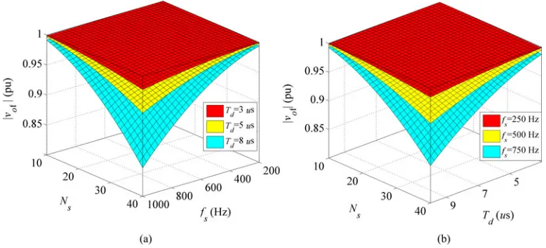
The per unit representation in (22) holds for all single- and three-phase configurations (phase-to-ground voltage). vofpu is graphed in Fig. 7 for different values ofNs,fs, andTd. As ex-pected,vofpudecreases with an increase in any of the three param-eters, with a minimum of 2/πp.u. when(Ns−1)Td = 1/2Ts, which represents a triangular-shaped output voltage.
The lower the fundamental voltage magnitude, the higher the load current for a given amount of power transfer, with subse-quent penalties in terms of efficiency, volume, and capital cost. Expectedly, the results show that the sacrifice in the fundamental modulation index with a quasi-two-level output is insignificant for an acceptable range of parameter values. This allows for a margin for various design objectives to be met. Proper design of each of the three parameters in (22) depends mainly on the op-erating voltage, control design, employed switches, and volume constraints.
Fig. 7. Fundamental output voltage of the Q2LC in terms of N,ωs, andTd. (a) For discrete values ofTdand (b) discrete values ofωs.
Fig. 8. Per unit magnitude of main harmonic components of the Q2LC output voltage, withfs = 500Hz.
magnitude is2Vdc/kπ (4 Vdc/kπfor a single-phase H-bridge)
with k being the harmonic order.
B. Dwell Time Range
Selection of the dwell time Td involves tradeoffs between
dv/dt stress, cell capacitor size, and fundamental output voltage.
The required dead timeTD B between the two IGBTs of each
cell as well as other switching delays and transit times become significant considering the small value ofTd. The total switching time of one cellTsc (IGBTs switch complementarily) can be
defined as
Tsc =td(off )+tf +tD B+td(on)+tr. (24)
For instance, the Infineon FZ1500R33HL3 3.3-kV 1500-A IGBT module has a total turn-on time oftd(on)+tr = 1μs and turn-off time oftd(off )+tf = 5μs [40]. When a dead time of 0.5–1μs is inserted,Tsc must be at least 6.5μs. Consequently,
the switching process of a cell must be initiated a timetd(off )+ tf before the cell is actually meant to alter its state.
The dwell time, however, is not bounded by Tsc, which is
beneficial for applications where higher frequency is required. For a dwell time Td < Tsc, cell switching becomes naturally
overlapped. Switching overlap in an arm means that the gating of
the next cell to switch is initiated before the currently switching cell has actually changed state.
The overlapped switching sequence with positive (charging) arm current is shown in Fig. 9, where the cells per arm are numbered in ascending order for simplicity. The actual order is determined by the employed capacitor balancing method. With negative (discharging) arm current, a cell capacitor is inserted (a step in output voltage) only when the respective auxiliary IGBT fully turns on.
C. Soft-Switching Characteristics
Fig. 9. Overlapped cell switching for dwell timeTd< Ts c. (a) NCS (SNCS)
sequence, and (b) CS (SCS) sequence.
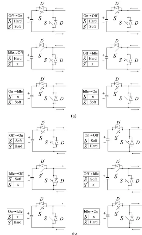
auxiliary IGBT Sturns on after the dead timeTD B with its
an-tiparallel diode conducting (soft turn-on). For the same terminal current direction, when the cell state changes from on to off, S undergoes soft turn-off, while S is hard switched. Once S turns on, Dbecomes reverse-biased and a short reverse recovery time is necessary. Therefore Dmust be a fast-recovery diode.
When the cell switches between on and off states under neg-ative current, S turns on and off under zero voltage and current, while Sis hard switched. When Sturns on, D becomes reverse biased and must be a fast recovery device. When a cell tran-sits between on and idle states, only the auxiliary IGBT Sis involved, and is hard switched under negative current and soft switched with positive current, as shown in Fig. 10. Similarly, when switching between idle and off states, only the main IGBT
S is involved, and it undergoes soft switching under negative
current and hard switching with positive current. Fast-recovery characteristics are required for both antiparallel diodes (Dfor transit from idle to off state with positive current and D for transit from idle to on with negative current).
The soft turn-on capability is of pivotal importance for switch-ing loss curtailment [14], [41]. Hard turn-off losses can be re-duced using passive lossless snubbers, although any form of discrete snubbering should be avoided, when possible, in or-der to reduce complexity and costs. Therefore, an augmented soft-turn off feature is undoubtedly a plus.
In a Q2LC phase leg, the switching-off arm—where cells states transit sequentially from off to on—experiences positive current flow when the phase current zero-crossing instant lags that of the phase voltage by an angleυ≥1/2ωsTt (inductive loading). Conversely, it experiences negative current flow when the phase current zero-crossing instant leads that of the phase voltage by an angleυ≥1/2ωsTt(capacitive loading).
Conse-Fig. 10. All possible state transitions of a half-bridge Q2LC cell with (a) Positive (charging) current, and (b) Negative (discharging) current.
quently, inductive loading will cause all auxiliary IGBTs of the switching-off arms to turn-on with zero voltage and current in a lossless manner. With capacitive loading, these IGBTs will hard turn-on, increasing switching losses.
The switching losses of the switching-on arm(s)—where cells switch sequentially to the off state—-depend on the switching sequence. With the CS sequence, the switching-on arm has all cells switching from on to off state. This state transition takes place with some current flow in the arm. In case of inductive loading withυ≥1/2ωsTt, this current flow is in the discharg-ing direction. Thus the main path IGBTs of the switchdischarg-ing-on arms experience soft turn-on, while the auxiliary IGBTs have a lossy turn-off, as displayed in Fig. 10. The direction of current flow in the switching-on arm(s) will be positive for capacitive loading withυ≥1/2ωsTt, resulting in hard turn-on of the main path IGBTs and soft turn-off of the auxiliary IGBTs.
[image:11.594.304.538.65.452.2]TABLE III
COMPARISON OFSWITCHINGCHARACTERISTICSUNDERDIFFERENTSWITCHINGSEQUENCES[↓=OFF,↑=ON]
regardless of the loading conditions. Note that transition of cells states from on to idle in the same arm—a period Ti before the output voltage transition—occurs at zero current with all the load current flowing in the other arm of the phase leg. In Fig. 10, the state transitions from off to idle and from idle to on are irrelevant to Q2LCs employed in DAB applications and operating under the presented switching sequences.
Table III summarizes the switching characteristics explained above, with the improvements offered by NCS over CS shaded in gray. As Table III confirms, NCS sequence will generate lower switching losses under capacitive loading than with the CS sequence. Furthermore, the turn-off losses of the auxil-iary IGBTs of the switching-on arm(s) under inductive load-ing are not present with the NCS sequence. A further study is needed to quantify the significance of the switching loss cur-tailment brought about by NCS sequence with regard to the extra common-mode oscillation and capacitor voltage ripple it triggers as compared to the CS sequence.
So far, one can conclude that regardless of the switching pat-tern, inductive loading is favored for a Q2LC in terms of switch-ing losses. This characteristic is used to define the soft-switchswitch-ing region for a Q2LC-based DAB. It will be illustrated with the aid of the space vector representation of the fundamental compo-nents of ac quantities, referred to primary (see Fig. 11a). Both Q2LCs will be inductively loaded withυ ≥1/2ωsTt(i.e., soft switched) as long as the ac current space vector lies within the shaded area representing an angular span ϕ−ωsTt. So for both converters to operate soft switched, ϕ > ωsTt is an essential operation constraint. Additionally, the dc ratio for soft switching of both converters must lie within the boundary defined by
ρh =
4π−3ωsTt 4π+ 3ωsTt−6ϕ
(25a)
ρl = 1
ρh
(25b)
whereρhandρlare the highest and lowest values of the dc ratio, respectively, for soft-switched primary and secondary Q2LCs. Equation (25) can be derived by settingip(θ=ωsTt) = 0and
[image:12.594.308.554.248.638.2]ip(θ=ϕ) = 0. The soft-switching boundary defined above is
Fig. 11. (a) Phasor diagram representing ac voltages and currents of a Q2LC-based DAB.[Superscript f denotes fundamental component], (b) equation (25) plotted against dwell time, and (c) equation (25) plotted against load angle.
[image:12.594.121.217.637.692.2]Alternatively, if the ac current vector lies within the angle
ωsTt surrounding the voltage space vector of either converter, this converter will operate in partial soft switching, with one or more cells per arm switching under capacitive loading (i.e.,
υ<1/2ωsTt). In Fig. 11a, an extended region including the partial soft-switching areas (an angle spanϕ+ωsTt) can also be defined. In this region a slightly higher range of dc ratio than that plotted in Fig. 11(b) and (c) is possible. This region is bounded byϕ=ωsTt, ip(0) = 0andip(θ=ϕ+ωsTt) = 0, yielding the dc ratio boundary values given by
ρh =
4π−3ωsTt 4π−3ωsTt−6ϕ
(26a)
ρl = 1
ρh
. (26b)
V. Q2LC OPERATIONWITHMODULATIONINDEXCONTROL
Modulation index control in a DAB converter enhances the capability of voltage regulation and power flow control [15], [42]–[45]. In a Q2LC, the sequential switching nature allows the fundamental voltage magnitude produced by the Q2LC be varied by a number of techniques. However, in practice, the vari-ation range will be limited relative to a standard MMC dc/ac converter. The main limiting factors are switching losses and harmonic content. Nevertheless, when utilized within a dc grid, the bridges of a front-to-front dc–dc transformer may not be required to operate at as wide range of modulation indices as a terminal dc/ac converter is expected to. Furthermore, the pres-ence of an ac transformer stage with on-load tap changers may help reduce the modulation index control range required to ac-count for steady state dc voltage variations. An exception to that is a faulty condition, where the nonfault-side Q2LC may have to operate in a current controlled mode to enable the healthy sections of the dc grid ride-through the fault/disturbance.
For a generic Q2LC design, (21) implies that the fundamen-tal voltage magnitudevof can be changed by varying the dwell
time Td (while mf = 1). As has been shown in Fig. 7, this change is limited except for higher values ofNsandfs. How-ever, further reduction ofvof can be produced by sequencing
some of the cells per arm at a dwell timeTdm higher thanTd
[see Fig. 12(a)]. Equation (18) can be applied to each set of cells having the same dwell time then summing to produce the fundamental output voltage and harmonic magnitudes. Clearly, the multislope waveform requires sizing the cell capacitance to the highest dwell time. Double or triple slope waveform can be produced to extend the control range and eliminate high order harmonics; however; on the expense of larger cell capacitors. “Slope modulation” may be considered the primary modulation index control technique. Additional auxiliary techniques may be employed in conjunction with slope modulation for a wider control range, if needed.
[image:13.594.341.505.68.424.2]A number of auxiliary techniques will be briefly ana-lyzed. These are denoted “interswitching modulation,” “clamp modulation,” and the conventional “phase-shift modulation.” Fig. 12(b) and (c) displays the modulated Q2LC output voltage (withmf <1) for two auxiliary modulation techniques. Note
Fig. 12. Modulated Q2LC output voltage. (a) Multislope trapezoid, (b) inter-switching modulation, and (c) phase-shift modulation.
that only auxiliary techniques—not the slope modulation—are regarded to act upon the value ofmf in (18).
A. Interswitching Modulation
In the interswitching modulation[see Fig. 12(b)], a controlled stepped dip is symmetrically introduced into the output voltage. The dip magnitude and time span are controlled to achieve the required modulation index. The dip magnitude isNmVdc/Ns,
whereNm is the number of dip steps(Nm ≤1/2Ns). The dip time is2NmTdd, whereTddis the step dwell time. Using (18), the p.u. magnitude of the kth odd harmonic component of the interswitching modulated output voltagevo(k) is given in (27).
Equation (27) is valid for single-leg, H-bridge, and multi phase Q2LC topologies
Vopu(k) =
⎧ ⎪ ⎪ ⎨ ⎪ ⎪ ⎩
2
Ns sin
kπ
2
(η−χ), Ns∈2Z+
2
Ns sin
kπ
2
(λ−χ), Ns ∈2Z++ 1 (27a)
where
χ= Nm−1
i
The base value for each harmonic p.u. magnitude is2Vdc/kπ
(4Vdc/kπfor the single-phase H-bridge). To achieve a certain mf, the following condition must apply to (27):
χ|k= 1 =
(1−mf)η|k= 1, Ns ∈2Z+ (1−mf)λ|k= 1, Ns∈2Z++ 1.
(28)
The condition in (28) can be realized by controllers. For example, with one of the two parameters Nm and Tdd held constant, a control loop can vary the other parameter within an intended range in order to follow themf command. Once the first control parameter reaches its limit with a nonzeromf error, a second control loop activates to vary the other parameter. The
mf command itself can be the output of a current-control loop.
B. Clamp Modulation
The clamp modulation method is similar to conventional MMC modulation index control [46]–[48], where the output voltage peaks at ±mfVop where Vop = 1/2Vdc for a
single-leg or a multi-phase Q2LC and Vop =Vdc for an H-bridge
Q2LC. For the latter structure, number of cells per arm in on state required to achieve a certain mf is given by (29), over a cycle. In (29), ||x|| is the value of x rounded to the nearest integer. From (29) in conjunction with (2) one can note that at least one cell per arm must remain in on-state such thatmf <1. This implies that load current always flows through the inserted capacitor(s); thus, a large cell capacitance is needed to retain acceptable voltage ripple. The required ca-pacitance increase may be significant even if the inserted cells per arm are cycled during operation. Furthermore, the val-ues the modulation index can take are discrete, thus reducing controllability.
C. Phase-Shift Modulation
In phase-shift modulation [see Fig. 12(c)], a phase shift
β > Tt is inserted between the switching functions NYon(t)
of the two legs of the single-phase H-bridge Q2LC such that they are no longer complementary. This introduces zero-volt intervals in each output voltage half cycle [43]. Zero-volt in-tervals can be inserted in the ac pole voltage of single-leg or multi-phase Q2LCs by splitting the transit periodTt into two halves with a time delay angle 2β. This way ac pole voltage transits for1/2Ttto zero, where it remains for an angle 2β(no cell state transition), then transits to the other dc rail voltage in 1/2Tt. However, the range of β will be narrower than an H-bridge converter to avoid significant increase of cell capac-itance. Using (18), for a phase shift ofβ= 1/2(π−σ),vopu(k)
can be expressed as in (30), which holds for single-leg, H-bridge
and multi-phase Q2LC designs
vpuo(k) =
⎧ ⎪ ⎪ ⎨ ⎪ ⎪ ⎩ 2 Ns sin kπ 2
ς, Ns∈2Z+
2 Ns sin kπ 2
ψ, Ns ∈2Z++ 1 (30a)
where
ς = Ns−1
i∈2Z∗+ 1
sin (1/2k[σ−iTdωs])
ψ= 1 2 +
Ns−1
i∈2Z+
sin (1/2k[σ−iT
dωs]). (30b)
Using (18) and (30), the phase shift angle required to produce a certainmf must satisfy the condition
η|k= 1 =
⎧ ⎪ ⎪ ⎨ ⎪ ⎪ ⎩ 1 mf
ς|k= 1, Ns ∈2Z+
1
mf
ψ|k= 1, Ns ∈2Z++ 1.
(31)
vpuo(k)is graphed in Fig. 13 for interswitching modulation and phase-shift modulation. Both graphs are developed with a Q2LC design, where Td = 5 μs, Ns = 20, and ωs = 1000π rad/s. These values result in a 1.5% drop in fundamental output volt-age before application of a further modulation technique (i.e.,
mf = 1). For this design, interswitching modulation employed withTdd= 10 μs and Nm = 1/2Ns= 10 achieves a funda-mental modulation index of about mf = 0.7. IncreasingTdd generates further reductions, but at the expense of larger cell ca-pacitances and switching losses. A study of the output waveform harmonic content (particularly low order harmonics) is impor-tant for power flow and transformer loss analyses. In Fig. 13(a), the third and seventh harmonic voltages may rise above 1 p.u. over some range, whereas the fifth and ninth remain below their base values over the shown range.
As introduced previously, the base value of each harmonic voltage is its corresponding value in a square wave of the same frequency and magnitude. In Fig. 13(b), the fundamental volt-age decreases while increasingβ. The same occurs to the third harmonic, which reverses polarity forβ >26◦. Other main har-monic components are less than their base values over the con-sidered range. Atβ= 0 (i.e., no phase-shift modulation), the per unit values of harmonic voltages are also below 1 p.u. due to the trapezoidal shape.
Theoretically, all three auxiliary modulation techniques can concurrently control the output voltage in conjunction with slope modulation. Practically, in terms of cell capacitance
NYon(t) = ⎧ ⎪ ⎪ ⎪ ⎪ ⎪ ⎪ ⎪ ⎨ ⎪ ⎪ ⎪ ⎪ ⎪ ⎪ ⎪ ⎩
Ns(1−mf)+
Ns(2mf−1)−1
i
u(t−iTd), 0≤t <Ns(2mf −1)−1Td
mfNs, Ns(2mf −1)−1Td ≤t <1/2Ts
mfNs −
Ns(2mf−1)−1
i
u(t−[1/2T
s+iTd]), 1/2Ts ≤t <1/2Ts+Ns(2mf −1)−1Td Ns(1−mf), 1/2Ts+Ns(2mf −1)−1Td+≤t < Ts
Fig. 13. Harmonic magnitudes of Q2LC output voltage atTd= 5μs,Ns= 20, andfs= 500Hz, with (a) interswitching modulation, and (b) Phase-shift
[image:15.594.50.289.515.603.2]modulation.
Fig. 14. Schematic for the reduced-scale single phase Q2LC.
requirement, interswitching, and phase-shift modulation tech-niques are favored over clamp modulation. When interswitching and phase-shift modulation techniques are merged with slope modulation, (27) and (28) evolve to (32) and (33), respectively
vpuo(k) =
⎧ ⎪ ⎪ ⎨ ⎪ ⎪ ⎩
2
Ns sin
kπ
2
(ς−χ), Ns ∈2Z+
2
Ns sin
kπ
2
(ψ−χ), Ns∈2Z++ 1 (32)
χ|k= 1 =
(1−mf)ς|k= 1, Ns ∈2Z+
(1−mf)ψ|k= 1, Ns∈2Z++ 1. (33)
Equations (32) and (33) offer at least five degrees of freedom for output voltage modulation design, namelyNs,Nm,Td,Tdd, andσ. An extra degree of freedom is implicitly present due to the variable dwell time of the slope modulation mode. Direct design constraints are cell capacitance size, switching losses, and ac transformer design and losses.
VI. EXPERIMENTALVALIDATION OFCONCEPT
Fig. 14 and Table IV summarize the layout and parameters of the utilized test-rig. With a 200-V dc source, a stepped out-put voltage of about±100-V peak drives a 10-A peak-to-peak load current (see Fig. 15). In Fig. 15(c), the cell voltages are
TABLE IV
OTHERPARAMETERS OF THESCALEDLABORATORYSETUP
Dwell time (Td) 25μs
Operating frequency 250 Hz Switching sequence CS
maintained within a±12% peak-to-peak ripple band for a 5-A peak load current, with 15-μF cell capacitance. This band can be reduced with higher capacitance for the same loading, as per (6). The load voltage transits in three uniform steps (a four-level waveform). Common-mode inrush current peaks at around 1.4 p.u. of the load current and will be minimal with proper de-sign of inductance/capacitance ratio. Circuit parasitic resistance rapidly damps common-mode oscillations, which quickly dis-appear after the voltage transition period. As predicted, the load current is decoupled from arm current oscillations. The results confirm that small cell capacitance and arm inductance is needed compared to conventional MMCs of similar power.
A power analyzer connected across the load and the dc sup-ply showed 95% efficiency. The primary source of the incurred sizable losses is the on-state voltage of low voltage IGBTs. For the employed IRG4IBC30UDPBF 17 A 600 V devices, this voltage constitutes a significant percentage of the device voltage rating, particularly since the IGBTs are operated at a fraction of their rated voltage and well below their current rating. In a practical MV or HVDC application, the on-state voltage/resistance of high-power high-voltage IGBT modules are insignificant against their rating, reducing the percentage contribution in conduction losses despite the higher number of IGBTs employed. Also, optimal conductor sizing and circuit routing is a characteristic of manufactured systems where stray components are minimized.
VII. DISCUSSION
Fig. 15. Experimental results from the scaled test rig. (a) 1 ms/div, (b) 250μs/div, (c) 1 ms/div.
may be sufficient. Also, stray resistance provides suitable damping. A further study needs to estimate the impact of fault current limiting, power reversal and start up requirements on cell capacitance and arm inductance sizes. A larger cell voltage ripple leads to larger common-mode current peaks, particularly with the NCS sequence. A larger common-mode current will in turn contribute to higher dc voltage ripple. Therefore, selection of cell voltage ripple band is strongly related to dc-side filtering.
Transformer design for medium and high voltages, even at the medium frequency range is challenging. Although the Q2LC provides acceptable dv/dt stress levels, issues like transformer core losses and the impact of parasitic components need to be addressed. Particularly, in upper medium and high voltage dc– dc converter designs, ac transformer efficiency will be of higher priority than its volume, which will allow designers to decrease the operating frequency towards lower ranges (<500 Hz). This postulate is supported when considering the physical clearance and voltage creepage distance requirements at such high voltage levels, which is likely to contradict any volume reduction. Note that, at very high- power levels, the use of three single-phase ac transformers may be unavoidable. Alternatively, a high-voltage Q2LC DAB may be split to several medium voltage modules with series, parallel, or series parallel connections to facilitate transformer design. In traction and dc distribution applications, at medium voltage levels, the frequency could be relatively in-creased for a smaller ac transformer stage.
The Q2LC structure utilizes double the number of IGBTs as an equivalent series-switch-array two-level converter. Although the auxiliary IGBT/diode pair does not require the same contin-uous current rating as the main IGBT/diode pair, the capital cost of a Q2LC is expected to be higher as the silicon area has in-creased. Nevertheless, the operation of each Q2LC cell involves only one IGBT in on-state at any instant. Except for the brief voltage transition periods, the Q2LC is effectively a two-level converter. As a direct result, conduction losses are expected to be similar. The soft-switching characteristics, on the other hand, have been shown in Section IV to be comparable to a two-level bridge in a DAB configuration.
Measurements and control are more complex in a Q2LC than in a two-level bridge, but not more complex than in a conven-tional MMC, due to structural similarity.
In principle, a Q2LC structure offers scalability and can be extended to ultra-high dc voltages without encountering the gat-ing or dv/dt problems impedgat-ing the extension of series-switch arrays. An ultra-high-voltage DAB-based dc transformer could be beneficial for dc fault isolation, which is one of the main ob-stacles impeding a multiterminal HVDC technology [9]. When the considered dc transformer is connected between two links of different dc voltages, dc fault at one side is not propagated to the other side [26]. Minimal current is fed into the dc fault and the dc fault appears as an ac fault to the non-faulted side of the dc transformer, where active power balance becomes the primary dc system stability concern.
VIII. CONCLUSION
The modular multilevel design of DAB converters was ana-lyzed. The multilevel DAB structure is meant to serve medium and high voltage applications. The modular design facilitates scalability in terms of manufacturing and installation, and per-mits the generation of an output voltage with controllable dv/dt. The modular design is realized by connecting an auxiliary soft voltage clamping circuit across each IGBT of the series switch arrays in the conventional two-level DAB design. With auxil-iary active circuits, series connected IGBTs effectively become series connection of half-bridge submodules (cells) in each arm, resembling a MMC structure. For each half-bridge cell, capac-itance for quasi-square wave operation is significantly smaller than typical capacitance used in modular multilevel converters. Also, no bulky arm inductors are needed. Consequently, the foot-print, volume, weight and cost of cells are lower. Four switching sequences were proposed and analyzed in terms of switching losses and operation aspects. A design method to size converter components was proposed and validated. Soft-switching char-acteristics of the analyzed DAB were found comparable to the case of a two-level DAB at the same ratings and conditions. Sim-ulation and experimental results were presented to substantiate the concept.
![Fig. 5.(a) Block diagram of a generic three-phase Q2LC based DAB con-verter, and (b) ac voltages and currents of one transformer phase referred to theprimary side [i′s is the secondary-side phase current referred to primary].](https://thumb-us.123doks.com/thumbv2/123dok_us/1589720.111694/7.594.42.287.64.325/voltages-currents-transformer-referred-theprimary-secondary-referred-primary.webp)
![CTABLE IIIOMPARISON OF SWITCHING CHARACTERISTICS UNDER DIFFERENT SWITCHING SEQUENCES [↓ = OFF, ↑ = ON]](https://thumb-us.123doks.com/thumbv2/123dok_us/1589720.111694/12.594.121.217.637.692/ctable-iiiomparison-switching-characteristics-different-switching-sequences.webp)