In Partial Fulfillment of the Requirements for the Degree of
Doctor of Philosophy
California Institute of Technology Pasadena, California
2007
c 2007
Acknowledgements
I would like to start by thanking the members of my committee, who have helped and supported me at various stages of my research. Professor Pietro Perona, my academic advisor, Dr. Bedabrata Pain, my research advisor who suggested a partnership with JPL and the CMOS imaging group, Professors Ali Hajimiri, Christof Koch, Alain Martin, and Dr. Bimal Mathur who gave me valuable feedback and perspective on my work.
This adventure would not have been possible without the help of the many people whose path I crossed during my years at Caltech and at JPL. On a scientific level, I would like to express my gratitude to Guang Yang who jump-started my research by teaching me proper design techniques as well as confidence in my work and abilities. Everyone in the Active Pixel Sensors group contributed to a friendly, supportive, and scientifically stimulating environment. Thanks to my long-time officemate, Pavani Peddada, I had a friend to keep me in track when the goal seemed so far away.
When I first arrived at Caltech, I had little more than a vague idea of what was lying ahead and no funding at all. I am indebted to Don Skelton for hiring me as an assistant for his physics freshman and sophomore laboratory courses as soon as I arrived in California. This lead to a partnership with the physics department that lasted until the end of my Ph.D., with the continued help from Frank Porter who always managed to squeeze me into his budget. These years of teaching, the other instructors I worked with, and most of all my students have taught me more about science and human interaction than I ever imagined possible. When Virginio Sannibale took over the supervision of the lab, I found myself with a great supporter. With his unfailing trust and encouragements, he helped me tremendously when I needed the flexibility to organize my teaching duties around my research and my deadlines.
Abstract
As imaging technology evolves, so does the need for accurate, low-power and high-data-rate low-level image processing in a variety of computationally intensive vision applications. These applications include optical-flow computation, autonomous navigation, object avoid-ance or intercept, real-time target tracking, and recognition. To reach this goal, a single chip was developed, which functions as a camera able to preprocess the image in real time. It processes images through a convolution filter with a user-chosen kernel.
One of the particulars of this project is to combine the processing unit with an active pixel sensors (APS) pixel array. This complementary metal-oxide semiconductor (CMOS) technology for building imager chips allows on-focal plane signal processing, as opposed to their charge-coupled device (CCD) counterparts that need to serially output the flow of pixels to an external processing chip. The filtering can therefore be implemented as a fast, low-power analog circuit.
Acknowledgements iv
Abstract vi
1 Introduction 1
1.1 On-chip image processing . . . 1
1.2 Outline . . . 2
2 Optical Flow for Hardware Implementation 4 2.1 Introduction . . . 4
2.2 Optical flow derivation . . . 4
2.3 Digital hardware resources . . . 7
2.4 Analog hardware resources . . . 10
3 Convolution 13 3.1 Image convolution . . . 13
3.2 Algorithm . . . 14
3.2.1 Overview . . . 14
3.2.2 Sum of products . . . 17
3.2.3 Accumulators . . . 17
3.3 Simulations . . . 20
3.3.1 System simulation . . . 20
3.3.2 Accuracy tolerance . . . 22
4 Digital Stand-Alone Implementation 27 4.1 Introduction . . . 27
4.3 Trade-offs . . . 31
4.4 Layout . . . 33
4.4.1 Memory . . . 34
4.4.2 Convolution unit . . . 35
4.5 Testing . . . 36
5 On-Focal Plane Implementation: Current-Mode Computational Imager 41 5.1 Introduction . . . 41
5.2 Imager . . . 42
5.2.1 Pixel implementation . . . 43
5.2.1.1 Current mode pixel . . . 43
5.2.1.2 Voltage mode pixel . . . 45
5.2.2 Readout circuit . . . 46
5.2.2.1 Voltage to current converter . . . 46
5.2.2.2 Cascode load . . . 51
5.2.2.3 Resistive load of the voltage to current converter . . . 53
5.2.2.4 Output of the readout current mirror . . . 54
5.2.3 Fixed pattern noise reduction . . . 55
5.2.3.1 Current memory . . . 56
5.2.3.2 Difference circuit . . . 57
5.3 Multiplying DAC . . . 58
5.3.1 Binary-scaled ladder . . . 60
5.3.2 Output scaling . . . 61
5.3.2.1 Time scaling . . . 61
5.3.2.2 Geometric scaling . . . 62
5.4 Accumulators . . . 63
5.4.1 Pipeline . . . 64
5.4.2 Single-cell structure . . . 65
5.4.3 Double-cell structure . . . 67
6 Design and Simulation 69 6.1 Introduction . . . 69
6.6.1 Single cell . . . 89
6.6.2 Double cell . . . 89
6.6.3 Pipeline . . . 91
6.7 Uncertainties . . . 96
6.7.1 Accumulator propagation of errors . . . 96
6.7.2 Circuit noise . . . 98
6.7.2.1 Current mirror . . . 98
6.7.2.2 Current memory . . . 100
6.8 Conclusion . . . 103
7 Implementation 105 7.1 Introduction . . . 105
7.2 Chip description . . . 105
7.3 Layout specifics . . . 109
7.3.1 Imager . . . 109
7.3.2 Multiplier . . . 113
7.3.3 Accumulator . . . 116
7.4 Growth prospects . . . 120
7.5 Micrographs of the chip . . . 120
8 Characterization and Verification 123 8.1 Introduction . . . 123
8.2 Imager . . . 123
8.2.1 Linearity, quantum efficiency, and conversion gain . . . 124
8.2.2 Temporal noise . . . 131
8.2.4 Spatial noise . . . 132
8.2.5 Dark current . . . 133
8.2.6 Spectral response . . . 135
8.2.7 Images . . . 136
8.3 Computation performance . . . 137
8.3.1 Multiplier . . . 137
8.3.2 Accumulator . . . 142
8.3.2.1 Single-cell module . . . 142
8.3.2.2 Double-cell module . . . 142
8.3.2.3 Pipeline . . . 144
8.4 Power dissipation . . . 145
8.5 Conclusion . . . 147
9 Conclusion 149 9.1 Summary . . . 149
9.2 Future work . . . 151
A Appendix 153 A.1 Matlab simulations . . . 153
A.1.1 Convolution algorithm using the pipeline accumulator . . . 153
A.1.2 9-stage pipeline accumulator . . . 154
1.1
On-chip image processing
While high-speed imagers with varying degrees of performance are being developed [1, 2], and high speed digital processors exist, signal transfer from the imager, and processing of images at a high update rate, as required in autonomous navigation or object-avoidance scenarios, remains a challenge. Existing systems involving CCD or CMOS imager arrays combined with an external computing chip [3, 4] are limited both by the sheer volume of data, as well as by the bottleneck of transferring the data serially from the imager to the processing chip. These limitations only get worse as larger and larger imaging arrays are being released regularly on the market. It is now common to find imaging systems with well over ten million pixels. Transferring such a large amount of data for external processing demands resources capable of handling the information.
On-focal plane systems on a chip [5] benefit from fully parallel computing which simplify the interaction between neighboring pixels but at the cost of reducing greatly the fill factor of the pixels. Communication between non neighboring pixels also becomes an issue. In addition, in-pixel digital or binary systems [6] do not take advantage of the full precision of the signal from the imager, as the space restrictions for keeping a manageable pixel size do not allow the digital precision needed for good-quality imaging. Multichip and digital systems also suffer from large power consumption [2, 6], and they lack the compactness required in some embedded applications.
basis. Due to this semiparallel approach, the data volume and bandwidth to transfer the signals from the chip to a postprocessing unit are vastly reduced without enlarging the size of the pixels and therefore do not compromise the quality of the images. This architecture enables efficient implementation of high-quality, real-time computational imaging systems. On-chip implementation of a general-purpose convolution filter allows identification in real time of areas of interests within the field of view without compromising signal integrity. On-focal plane integration of image preprocessing allows an efficient implementation of a variety of computationally intensive applications such as autonomous navigation, object avoidance or intercept, and recognition.
1.2
Outline
Optical flow calculation in real-time systems is a computationally intensive task, yet com-mon in vision applications. Fast, low-level execution before the transfer of the image to an external processor alleviates the load on the processor. However, the calculations re-quire the evaluation of spatial as well as temporal gradients which are not computed easily in hardware. An optical flow algorithm that is appropriate for hardware implementation (either analog or digital) is described in the second chapter, also with the benefits from a parallel first stage to reduce the load on digital circuits and produce a more compact design. At the heart of the optical-flow computation is the evaluation of convolutions with known kernels. The third chapter explains the basics of convolution and why it is a costly operation in circuit development. The term “cost” is defined, and an algorithm taking advantage of the semi-parallel architecture of active pixel sensor imagers is presented. Again, the algorithm is appropriate for both analog and digital implementation. Simulations on real images are shown to illustrate the correctness of the processing.
The design phase of the analog convolution chip is described in chapter six. The operat-ing conditions of each of the circuit subblocks is analyzed and the correspondoperat-ing simulation results are presented. The various interfaces between subblocks, which ensure proper trans-mission of the information in the entire chip are explained. Influencing the design decisions are the calculations on the derivation of the main noise sources and their propagation throughout the chip. They are therefore also part of this chapter.
The layout of the chip directly impacts the performance and therefore plays an important role in the chain of events to create a circuit. The seventh chapter goes through the specifics of laying out the analog blocks, the floor plan and the choices made to ensure a compact fit as well as good operation due to proper layout techniques ensuring good matching between transistors.
The fabricated computational imager chip was tested to evaluate the performance of both the imaging capabilities and the computation units. Test techniques specific to each circuit element are shown in chapter eight. The result of the tests are also detailed as integrated test structures allow separate testing of all the independent blocks.
Chapter 2
Optical Flow for Hardware
Implementation
2.1
Introduction
Determining the optical flow of a video sequence consists of extracting the changes in a series of images. It implies a system capable of finding the direction and velocity of the image at each pixel location. Optical flow determination is a common and fundamental image-processing task. It is used in a variety of vision applications. Examples include robotic vision systems [9], robotics [10], autonomous vehicle navigation, object avoidance or detection, and medical imaging [11]. However, an optical flow algorithm is not trivial to implement and is a computationally intensive tack. This problem can be approached in three different ways [12] depending on the application and the type of implementation: the frequency-based analysis [13] which extracts the frequencies of high energy, matching algorithms [14] where the distance between frame is computed, and the gradient method [14–16]. The gradient method was chosen and is described below because it can yield an algorithm that is well suited for hardware implementation.
2.2
Optical flow derivation
The variables Ex and Ey represent the spatial gradients of the image in the x and y direction respectively and Et is the temporal gradient. They are all also evaluated at the current pixel location(i, j).
The factor λ2 is a smoothness factor that can be chosen depending on the specific application.
To find the optical flow, we are solving equation (2.1) for
u
v
at every pixel location
in the image. We first need to estimate the laplacians ∇2u and ∇2v as functions of the current and previous image frames and solve for u andv.
To compute the laplacian, we introduce ¯u and ¯vsuch that:
∇2u=k(¯u−u),
∇2v=k(¯v−v),
wherek = 3.
The laplacian can now be approximated by applying a discrete kernel to the u and v
neighborhoods. [16–18] ¯ u=
1/12 1/6 1/12 1/6 0 1/6 1/12 1/6 1/12
∗
ui−1,j−1 ui,j−1 ui+1,j−1 ui−1,j ui,j ui+1,j
ui−1,j+1 ui,j+1 ui+1,j+1
¯ v=
1/12 1/6 1/12 1/6 0 1/6 1/12 1/6 1/12
∗
vi−1,j−1 vi,j−1 vi+1,j−1 vi−1,j vi,j vi+1,j
vi−1,j+1 vi,j+1 vi+1,j+1
u= ¯u−Ex· Eαx2u¯++EE2yv¯+Et
x+Ey2 ,
v= ¯v−Ey· Eαx2u¯++EE2yv¯+Et
x+Ey2 ,
(2.2)
whereα2= λk2.
Note that to evaluate the optical flow, it is necessary to already know its value (¯uand ¯v
depend onu andv). The calculation is therefore an iterative process which is not ideal for
real-time hardware implementation. A good approximation is the corresponding
u
v
from the previous frame. To give a reliable answer, the algorithm requires that the optical flow is assumed to not change much in time from one frame to the next.
To implement the above solution in hardware includes some degree of parallelism to speed up the computation without affecting the accuracy.
The steps to follow to reach a solution for equation 2.2 for two available frames are:
1. Gradient and laplacian are processed in parallel.
(a) Gradients Ex, Ey: spatial gradients in x and y. Both nearest neighbors would be used for a second-order approximation:
Ex=I1,0,0−I−1,0,0,
Ey =I0,1,0−I0,−1,0.
(2.3)
Et: temporal gradient. Only the previous frame is used. It is a first-order approximation so only one previous frame needs to be stored in memory.
¯
v=
1/6 0 1/6 1/12 1/6 1/12
∗
vi
−1,j,−1 vi,j,−1 vi+1,j,−1 vi−1,j+1,−1 vi,j+1,−1 vi+1,j+1,−1
.
With these elements, obtaining the optical flow is a straight forward process as we follow
equation 2.2 to compute new values for the vector u v .
To simplify the hardware implementation, in the next steps we break the equation down and introduce several intermediate variables that eventually lead to the final result:
2.
D =α2+E2
x+Ey2
P =Exu¯+Ey¯v+Et
3.
Px=Ex·P
Py =Ey·P
4.
Rx= PDx
Ry = PDy 5.
⇒
u= ¯u−Rx
v= ¯v−Ry
2.3
Digital hardware resources
is done while the next operator is still working on the current pixel position.
Assuming an entirely digital implementation, the cost of the algorithm is estimated in terms of resources needed. Resources are defined as being basic digital operators such as adders or multipliers. Depending on the precision sought, they can be implemented as any size words, their complexity growing accordingly. For example, a 3×3 convolution unit is equivalent to nine multipliers and eight adders. Table 2.1 shows the step during which each operator must perform its calculation such that the flow is not perturbed and shows the cost associated with its implementation.
Use of prior knowledge of the convolution coefficients can be an efficient way to reduce the complexity of the circuit but at the cost of making any evolution or modification of the algorithm difficult or not possible. Two aspects of the convolution operators are worth noting.
The matrix operation to calculate both ¯uand ¯vin equation 2.5 is a standard convolution which allows for the recycling of the convolution hardware. The cost of sharing is the serialization of the process (only one operation can be done at any given time) and the need for a router to guide the data flow for theu andv parameters into the same operator. The kernel used in both convolutions are identical, so even the coefficients storage can be shared directly.
Also, in order to calculate the laplacian, the convolution kernel is fixed and can therefore be hard-wired, sparing the cost of a full, generic multiplier. The middle coefficient being ”0”, the operator only has to work with eight parameters for a 3×3 window. The trade-off is that no modification of the kernel would then be possible, including to change the window size to smooth the image for estimating the gradients [19] or the use of a different kernel for the laplacian. [18]
2. P Two multiplications and 3-term adder
3. Px, Py Two multiplications
4. Rx, Ry Two divisions
5. u, v Two differences (adders)
In addition to the arithmetic operators listed in table 2.1, the cost of the circuit also includes the use of memory to store the neighboring pixels (or the partial products) for the convolution operator. The algorithm also makes use of the data from the previous frame to estimate the temporal gradient when solving for equation 2.4 so each frame must be stored in a memory for retrieval during processing of the next incoming frame. A FIFO memory of one frame size is very well suited for such purpose. The need for the nearest neighbor in both the xand y direction adds one line to the memory needs.
Similarly, the laplacian of equation 2.5 uses the results from the previous frame for both the ¯u and ¯vterms. Their values must be retained for an entire frame, with an extra line for the neighborhood, adding to the overall memory requirements:
M emory needed= 3×width×(height+ 1), (2.6)
where each memory point is an eight-, twelve- or sixteen-bit word, depending on the analog to digital converter used in the digitization of the pixels.
[image:19.612.130.511.104.325.2]storage requirements. Large temporal changes in the image or complex video scenes would require more complicated techniques such as a multi-scale approach [20,21]. A second-order approximation would require both nearest neighbors and would therefore require two frames to be stored while introducing a full frame latency.
However, although the implementation from Mart´ın et al. [15] uses a first-order approx-imation of the derivative for both temporal and spatial gradients, this rough approxapprox-imation is not so beneficial when dealing with the spatial gradients since the nearest neighbors are readily available in x with a one-pixel latency and in y with a one-row latency as in equa-tion 2.3. The added resources are one row in the memory, and the arithmetic resources are equivalent. A wider windows for the spatial gradient and laplacian results in increasing the memory to accommodate the larger neighborhood and increases the size of the convolution engine.
2.4
Analog hardware resources
The implementation of the image flow calculation in a fully digital circuit as described above suffers from several constraints that impair the circuit and can be improved on by introduc-ing some elements of analog circuitry when they can help the performance, compactness or integration of the circuit.
Figure 2.1: Example of a three-layer-stack interconnection: pixel array, analog transforma-tion and analog to digital conversion interconnected with deep vias.
one row at a time access to the image, which can still be used and have the advantage of allowing large circuits without expanding the overall footprint of the chip. Computing circuits that are typically developed inside the pixel site [25–30] can be relocated to a lower layer with no modification.
Although inserting a fully parallel analog layer as the initial low-level computation does not affect the output flow-rate of the chip after digitization, it opens the door to new possibilities that eventually lead to higher performance and eventually to a faster outflow of data. The two most intuitive ways to take advantage of this are to allow insertion of extra processing on the fly and to be able to preselect pixels or regions of interest before digitizing so the serial flow of digital information only handles a smaller amount of data.
Cell Digital area Analog area
8-bit multiplier 120,000 µm2 5740 µm2
One-pixel memory 15,600 µm2 615 µm2
9×9 convolution 5.88 mm2 to 16.8 mm2 0.1 mm2
Table 2.2: Area comparison between digital and analog cells
presented in chapter 7.
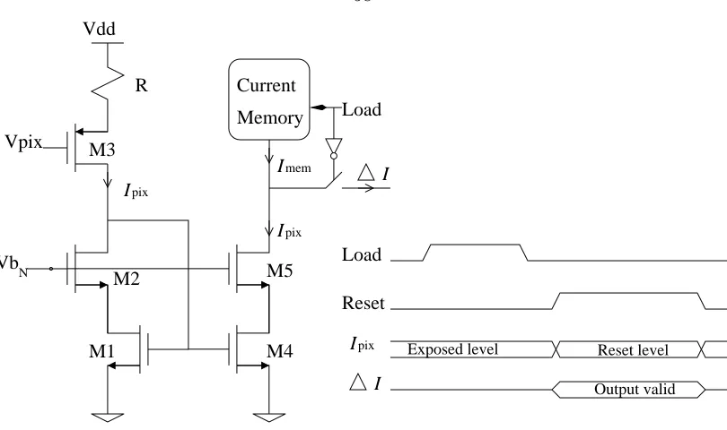
Note that only the arithmetic units to estimate the convolution are included in this estimate. The area needed to implement the memory used to buffer the previous frame also varies depending on the nature of the storage elements. A single capacitive memory cell is used to store an analog signal. The current memory cell presented in section 5.2.3.1 only occupies 615µm2 in the layout as shown in the bottom of the pixel analog readout circuit
layout in 7.5. The digital memory on the other hand requires one memory cell per bit of data. A D flip-flop as used in the chip presented in the next chapters uses an edge-triggered clock to set the memory. It occupies an area of 1950µm2 on the layout. Assuming eight-bit analog to digital conversion, each pixel or basic element would be encoded using eight bits. An eight-bit word therefore occupies 8×1950 = 15600µm2, which is 25 times larger than its analog counterpart. Custom layout geared toward compact optimization (e.g., using non-overlapping clocks schemes) would result in slightly smaller footprint but would not make up for such a difference.
3.1
Image convolution
The convolution of two functionf andg, notedf⊗g, is the measure of the overlap between the two signals. In the case of images, it represents the similarity of two patches. Convo-lution of an image with a smaller kernel is done by repeating the basic operation on the neighborhood of all the pixels of the image. The resulting image has the same size as the original and shows the locations where the kernel is visually similar to the image. Convolu-tion is used as a stand-alone operaConvolu-tion in digital filters such as orientaConvolu-tion filters, low-pass and smoothing filters, or matched filters for tracking and recognition applications. It is also used as part of a more complex computation like the optical flow estimate described in chapter 2 where it is used to calculate both the spatial and temporal gradients of sequences of images.
Let I be an image of arbitrary size. The general expression for discrete convolution [32, 33] at location (x, y) in the image I with a kernel K of size n×n is given by the expression:
C(x, y) = (I⊗K)|x,y = n−1
X
i=0
n−1
X
j=0
Ix−n−1
2 +i,y−
n−1
2 +j×Ki,j
.
simpler as it only handles a small amount of data, it is also well suited to the goal of hardware implementation. Each pixel of the convolved image being derived independently of all the others, it implicitly introduces the concept of parallel processing that will be exploited when designing the circuit.
I⊗K= n−1
X
i=0
n−1
X
j=0
(Ii,j×Ki,j) (3.1)
Equation 3.1 is only a rewrite of the general expression and therefore does not affect the rendering of the output image. Its use is justified by the algorithm development which becomes more intuitive when approached at the pixel level, as detailed in section 3.2 below. Some examples of image convolution with different kernels are shown in section 3.3 on simulation where a Matlab implementation of the algorithm described in the next section of this chapter is presented.
3.2
Algorithm
3.2.1 Overview
Implementing the convolution algorithm on a chip requires that the circuit be well suited to the system it is going to be integrated in and its operation. A hardware-oriented algorithm had to be developed that would take advantage of both the environment used (analog or digital, system on a chip or external processing system) and the interface (serial, parallel or semi-parallel) with the components of the imaging setup. What is meant by “setup” is the complete system interfacing an imager, either off the shelf or custom CMOS or CCD pixel matrix, with the convolution circuit operating in the digital or analog domain. Depending on the type of imager and mode of operation, the information from the pixels can be handled by a computation unit in three ways:
of the pixel matrix. Some computation or memorization can still be done inside the pixel [39]; it has the advantage of being able to keep the fill factor large while a column-parallel readout allow semi-column-parallel computation. Line buffers or stored partial results are used to use information from neighbors in different rows. [40–42]
The data flow in the convolution circuit is initialized in the pixel and therefore defines the interface to the first stage of the computation element. Since the final application for this project is an integrated fully custom active pixel sensor which operates in column-parallel mode, the algorithm uses this format to take advantage of that scheme rather than buffer the whole frame (or part of the frame) before starting computation as a generic processor. On the contrary, the digital implementation of the convolution chip receives a serial flow of pixels from an external imager. The incoming pixels are buffered until enough information has been read and is ready for use in the calculations. See chapter 4 for the details and specificities of the digital circuit.
In a column-parallel imager architecture, all the pixels of a row are made available at the same time to the readout circuit. They are kept valid for the entire time of the processing, until the next row is addressed. They are then replaced by the new incoming pixels which are in their turn sent to the readout circuit and the computation units. In contrast, the convolution kernel is a constant for a given frame and can be accessed at all time, allowing the realization of a pipeline architecture in the row direction.
Figure 3.1: Semi-parallel architecture: convolution block diagram
convolution unit is described in detail in the next sections. Identical structures operate in parallel to compute the transformation of every column of the imager.
Neighbors on the same row (horizontal neighborhood) are all read out together along with the entire row. They are used simultaneously for the calculating the convolution in nine columns. In the event of an analog system, care must be taken to not attenuate the signals during this multiple readout sequence. The product with each row of the kernel can occur at this point as well as the inner sum of equation 3.1 which is the sum of the pixel-wise products over the same row. In the accumulators the partial results are combined with those obtained from the rows previously read-out, so the vertical neighborhood is included in the outer sum as in equation 3.1.
The products obtained from the same line of the kernel are involved in the same con-volution calculation and can be immediately combined by summing them right after the multiplications. This direct sum of product approach keeps memory resources lower than if all products had to be memorized before the sum over the entire window is computed. The nine remaining partial results will be used when reconstructing the convolution for the window centered on different pixels of the same column when enough rows have been read out and the fill window has been multiplied and summed in the same way but against different rows of the kernel.
During readout, the part of the image that is available (one row) is a one-dimensional array, while the convolution operation requires a two-dimensional window to be used. The convolution window is reconstructed with the addressing of subsequent rows of the image. Each row is only read once but still must be utilized for the calculation of all the convolutions in which window it appears. Each row is therefore duplicated several times and combined with each row of the kernel to generate the partial products for each position that will be used. The duplication of the pixels from the imager and the separate processing for each kernel row is shown in the diagram of figure 3.2.
3.2.3 Accumulators
At the end of the first phase, the inner sum of products of equation 3.1 is computed for the current row, the outer sum (sum over different rows) remains to be reconstructed in accumulators by combining some of these partial products with those from previous rows and saving some for use with rows still to come.
imager.
Another important consideration is the need to handle a large signal range. When doing arithmetic in either the digital or the analog domain, signals are limited at both ends of the range. In the digital domain, information gets lost when small signals are rounded to a digital binary number and large values get clipped to the maximum number allowed for the allocated bit space. In the analog world, the noise level and saturation as well as non-linearity also restrict the range that can be used for transmitting information. The increase in signal strength is limited at each stage by averaging the result while preserving the same weight on each input.
LetXjthe output of thejthpartial product from the multiplication and inner sum stage, created when processing thejth row of the window on which the convolution is performed.
Xj is also input to the accumulator. Equation 3.2 summarizes the actual calculation that is performed, wheren is the number of rows used. (The kernel is ann×narray.)
I⊗K
n = 1 n n+1 X j=1
Xj (3.2)
To reconstruct this equation in a pipeline form, each stage incorporates its input from the sum of products from its corresponding kernel row into the average calculated so far. A weight correction, shown in equation 3.3, is done to preserve the equal influence of each parameter and to achieve averaging by the number of rows. When expanding it fully, the average form of equation 3.2 appears.
Pj i=1Xi
j =
j−1
j
·
Pj−1
i=1Xi
j−1 | {z } f rom previous stage
+
1
j
·Xj (3.3)
ripple through the same number of stages. While the first one, labeled X0 in the figures,
is scaled and transfered through all nine elements, the last one is only processed once. Although it makes no difference in the equation, the noise and uncertainties from all the operators will not affect the various inputs in the same way. The last one will have a greater influence on the final result. The robustness of the algorithm to this asymmetry is looked into in section 3.3.2. The noise analysis of each analog computational element and propagation of errors inside the accumulator are studied in section 6.7.
The simplified block diagram of the complete pipeline, figure 3.4, uses the same variables as the sum of products of figure 3.2, which interconnects with the pipeline. These two diagrams summarize the full architecture for hardware implementation of the convolution on one column. Further details on the sub-blocks of the design depend on the type of circuit being developed. Software simulation of this system is described in section 3.3.
Actual hardware implementations of the convolution algorithm have also been fabricated and tested: a stand-alone digital system is presented in chapter 4, and an analog circuit is studied in detail in chapter 5 and following.
3.3
Simulations
High level system simulation were run to illustrate the effects of various convolution filters on images. The proposed algorithm was implemented using Matlab, rather than the embedded convolution function. This not only validated the algorithm through simulation, but also performed various tests on the robustness of the algorithm and analyzed the propagation of uncertainties from stage to stage.
In the first part of this section, the convolution of an image with various different templates is shown. No noise is added to the system, so the ideal case is portrayed, and the effect of various filters is shown. Then, random and systematic uncertainties are inserted at various stages of the algorithm simulation, and their effect on the final output is shown with emphasis on the propagation of the errors and the robustness of the system.
3.3.1 System simulation
simulations show the transformation of the input image when applying a kernel with the convolution algorithm described in this chapter. The Matlab source code used to generate these results is shown in appendix A.
The first validation test is to verify the efficiency of the neutral element of the convolution and to obtain a filtered image identical to the input. When only one of the pixels of the kernel is non-zero, the image is not modified through convolution. It is only scaled and shifted, depending on the value and position of the remaining pixel. The identity kernel used in figure 3.5 uses the central pixel, so no shifting occurs, and its value compensates for the scaling taking place in the accumulator. The filtered image, shown in 3.5(b) is indeed identical to the original image.
Blurring can be achieved with a uniform kernel as in figure 3.6(a) where all the pixels of a 9×9 neighborhood are averaged by the filter. Gaussian kernels allow for a more subtle smoothing of the image, depending on the standard deviation σ used to generate them. Figures 3.7 and 3.8 show examples of such smoothing with two values forσ. As the value used for σ increases, the Gaussian kernel becomes less sharp and the images get more and more blurry.
Although the hardware implementation presented in chapters 4 (programmable digital system) and 5 (analog circuit) do not use signed operators, subtraction is a minor extension to the circuits and is already planned for in the pipeline algorithm which makes no as-sumption regarding the sign of the kernel parameters. Two examples of filters using signed operators are shown in figures 3.9 and 3.10 with first-order derivatives in the horizontal and vertical directions.
3.3.2 Accuracy tolerance
The reliability of the system depends on how well it is able to handle undesired variations from the ideal scenario. When dealing with arithmetic circuits, uncertainties may appear at any stage of the computation, so it is important to be able to predict their influence on the final results.
0 2
4 6
8 10
0 2 4 6 8 10
0 50 100 150
(a) Kernel (b) Output image
Figure 3.5: Identity filter: output image identical to the original
0 2
4 6
8 10
0 2 4 6 8 10 254 254.5 255 255.5 256
[image:33.612.127.529.99.325.2](a) Kernel (b) Output image
0 5
10 15
20
0 5 10 15 20
0 50 100 150 200 250 300
[image:34.612.127.527.105.329.2](a) Kernel (b) Output image
Figure 3.7: Gaussian filter: σ = 1.5 pixels
0 5
10 15
20
0 5 10 15 20
0 50 100 150 200 250 300
(a) Kernel (b) Output image
[image:34.612.126.529.429.648.2](a) Kernel (b) Output image
Figure 3.9: Horizontal edge detector
(a) Kernel (b) Output image
such operators are available and commonly used in microprocessors, they are complex and yield large designs. [43–46] To minimize rounding errors, the division at each step of the accumulator from equation 3.3 is not performed until the end of the pipeline where averaging occurs for all steps at once. Overflow in the pipeline is prevented by an adequately sized internal data bus. Section 4.3 describes the trade-offs specific to the digital implementation of the convolution algorithm.
The range of signal in the analog circuit is not expendable as easily in analog circuits. Although the bus size is constant, the level has to remain inside the linear region of operation of the operators. This is where scaling at each stage becomes critical to keep the analog sig-nal from growing into saturation. The rolling averaging of equation 3.3 solves this problem but amplifies the asymmetry of the error contribution inside the pipeline accumulator.
Implementation
4.1
Introduction
A general-purpose filter can be built on a variety of circuits, each tailored to specific ap-plications. A fully analog design is presented in the next chapters that incorporates the filter on the imager chip. An implementation of the same algorithm onto a fully digital circuit uses well-defined elements that are easy to set up. It provides a reliable testbench for validation of the algorithm as well as grounds for comparison of the various systems.
Microprocessor-based computers allow fast integration that is valuable for test and val-idation of the algorithm. With the use of a high-level programming language, they are easy to program, fully reconfigurable and operate at speeds that make them the best choice for many applications. Because of their physical size, however, they are ill suited for miniature environments and cannot meet power restrictions of many embedded systems.
The more practical implementations for compact, real-time image processing units call for more specialized components. Digital signal processors have been a platform of choice for many imaging systems. [47, 48] As general-purpose processors, they are also programmable and only require software-level development, making their turn around and reconfiguration very fast. They are also often equipped with specialized interfaces for data transfer which the full microprocessors lack. This is vital in real-time image processing due to the amount of data that needs to be transferred to and from the DSP.
can be implemented and no resource limitations, but unlike processors they cannot be programmed or reconfigured easily. The development time is much longer and the price much greater. The finished product is however the best tuned for the application since it carries no overhead or unused circuitry. Algorithms for convolution on digital VLSI chips have been developed and tuned using pipeline architectures, parallel computations or systolic arrays. [49, 50]
Field programmable gate arrays offer an attractive traoff between cost, ease of de-velopment and speed. Although they are made of predefined logic cells, they have few high-level functions and do not suffer from large overhead as DSPs and micro-processors do. Since they are designed in a similar way to full-custom circuits, they are a platform of choice for research and development before fabrication of integrated circuits. This is why algorithms for FPGAs have been studied extensively, either as proofs of concept or as final products. [35, 51–54]
Digital designs using standard CMOS logic can be implemented on the imager chip which uses the same technology. However, the test setup being developed would not be actually fabricated on an integrated circuit. The design is therefore made using the Verilog hardware description language which is first simulated as a behavioral model. It is then compiled and uploaded onto a reconfigurable FPGA for fast and efficient validation of the code and of the algorithm in a real test environment. The final step for a full-custom circuit is to synthesize the Verilog program to produce a full layout of the chip, ready for fabrica-tion. Each step of the design flow adds new information that is used in simulation such as timing restrictions and resources allocated. While the FPGA implementation validates the accuracy of the algorithm, it is the final layout that shows the actual resources used if it were to be fabricated.
FPGA / ASIC
Figure 4.1: Digital implementation block diagram
4.2
Algorithm
The convolution algorithm described in section 3.2 was developed for the purpose of hard-ware implementation. No assumptions regarding readily available building blocks were made and the drive was to minimize the cost of the algorithm in terms of resources while maximizing the parallelism of the data flow. The design process also did not assume which type of hardware implementation would be used. As a first approximation, the same factors have to be taken into account whether a digital circuit or an analog circuit is to be produced and the same trade-offs have to be considered in both cases. Therefore the same algorithm is implemented in both circuits. The specific implementation details of each approach do vary however. The trade-offs to be considered are different and will be discussed separately in section 4.3.
rendered.
The resources needed are not limited to the memory cells used to store the partial products which grows linearly as a function of the imager width and the kernel height, but also include arithmetic units for the actual convolution to take place. For each column computing unit, a choice had to be made between a fully parallel structure or a semi-parallel one. With the fully semi-parallel approach, as many multipliers as there are pixels in the kernel are necessary. (81 8-bit multipliers for a 9×9-pixel kernel) This is the most efficient design in terms of speed of execution but expectedly produces large layouts due to the redundancy of the hardware produced. In the semi-parallel implementation, the resources are re-used constantly in the processing of the columns. It is the width of the kernel only that determines the number of multipliers, not the product of the width by the length. Only one multiplier per column in the kernel is needed and provides nine partial products for each convolution computation.
Both options implement the same algorithm and therefore share the same structure as shown on the block diagram, figure 4.1. The multipliers and accumulators are wrapped in a pipeline implemented as a state machine. The difference between the two implementations are in the number of multipliers used and the latency introduced to ensure availability of the products at the stage they are needed in the pipeline. The sequence of events is common to both implementations and is made of four steps that are repeated for each pixel provided by the imager.
Multiplications. Prow(K·I). The pixel neighborhood is multiplied pixel-wise with each row of the kernel. The results of the same rows are added to each other, producing nine sums of products that will each be used in a stage of the accumulators.
Read from RAM. The contribution from the previously calculated partial products that correspond to the accessed column is needed so they need to be extracted from the memory.
design. A recurring issue touching digital computational units is the width of the data bus that needs to grow with each operation to avoid overflows and loss of information. A worst case scenario approach was taken for the internal buses so the width at the output of each multiplier or adder can accommodate any result. An internal bus of up to 20 bits guarantees that no overflow should occur during normal operation. The input range of 8 bits is restored for the output by post-computation division. Although it would keep the bus width constant and largely reduce the internal wiring, scaling is not done on the fly to avoid handling small numbers that can round to zero when using integer-based operators rather than floating-point divisors. On the algorithm level, the averaging factor of equation 3.2 is not done at each step of the accumulator as shown in the block diagram of figure 3.4 but rather at once after the complete accumulation has occurred. This is the only major difference with the analog implementation which required the signal range to remain in the linear region for every element, as is described in chapter 6 on the design requirements.
Digital Circuit Clock
Frame rate (Hz)
Row Clk (kHz)
Pixel Clk (M Hz)
Col-parallel (kHz)
Full Circuit (M Hz)
16-column Blocks (M Hz)
1 1 1 30 30 0.48
10 10 10 300 300 4.80
30 30 30 900 900 14.4
60 60 60 1800 1800 28.8
100 100 100 3000 3000 48.0
Table 4.1: Clocks for a megapixel imager (1024 rows and 1024 columns): full circuit with one convolution unit per column, one for the whole chip and one per block of 16 columns.
duplicate these resources into each column and obtain a much more efficient design in terms of speed of operation. The size of the circuit, however, becomes unmanageable as the whole arithmetic unit (which includes the multipliers as well as the accumulators) is multiplied by the number of columns in the imager.
The operating speed of the digital circuit does not justify the use of so much hardware. The flow of pixel from the imager is regulated by a pixel clock which is itself a function of the frame rate: CLKpix = CLKheightrow = (widthCLK×f rameheight). The frame rate can easily be changed
but for practical reasons, only small variations are possible. When the frame time decreases, less light is integrated in the imager so the image gets darker and the quality is affected. It can be compensated by increasing the light level and opening the aperture, but only on a small scale.
The information summarized in table 4.1 shows the two extreme cases and the suggested trade-off in terms of operating speed of the digital circuit. The data shown assume a 1k× 1k-pixel imager is used and attached to the convolution units as described here while operating at various frame rates. Processing each pixel requires eight memory accesses in read mode, and an extra 13 cycles delay for the pipeline dividers and nine memory accesses in write mode. The total of 30 cycles is therefore the minimum computation time for this algorithm. The memory modules used in the prototype use a two-cycle read and write scheme that brings the computation time to 54 cycles. The optimal case of 30 cycles is used as a reference in table 4.1 as one-cycle memories are readily available.
not practical for this type of circuit. As a reference, currently available FPGAs only allow up to a few hundred mega-hertz. More specifically, the Spartan-3 chip for Xilinx that is used in the prototype is rated for an internal maximum speed of 300M Hz. Digital signal processing chips can operate at a faster rate but would eventually face the same issue with fast frame rates (≥100f ps) or larger imager arrays.
The suggested trade-off for hardware implementation is to use a block-parallel architec-ture where the output of the imager is split. Several convolution units are implemented, each in charge of handling the data from 16 columns. Each convolution units operate in parallel, and the serialization only includes 16 pixels. The operating frequency remains in an easily manageable range for normal imaging operation while using significantly less resources.
4.4
Layout
A description of a single convolution unit was written in the Verilog HDL so a prototype could be built. The program was synthesized with the Xilinx library to produce a working setup on a Spartan-3 FPGA and also synthesized with the Mentor Graphics tools to generate a netlist and a standard cells-based layout. The FPGA uses predefined cells that perform a function when properly interconnected. The resulting implementation is sub-optimal and only serves the purpose of validating the code and the algorithm while quickly producing a working prototype. The netlist and layout, however, give a more realistic estimate of the resources needed in terms of number of logical gates and flip-flops and in terms of silicon area for fabrication.
validates both the algorithm and the digital implementation approach. It was discussed in section 4.3 on the trade-offs faced during the design phase that the possibility of parallelism is important for the viability of the system. This property is preserved with the designed cell as it is trivial to add more processing units in parallel in this configuration: the same computation cell needs to be arrayed and wired to various sub-sections of the imager. This re-wiring is, of course, only possible in the case of a system on a chip where the imager and the processor are on the same chip. In the case of multi-chip systems in which the imager provides the pixels as a serial flow of data, a pipeline is needed with a controller so processing starts on the first pixels of the row before the whole row is made available.
4.4.1 Memory
The memory requirements discussed above already included all that is needed for full frame processing and therefore do not change when parallel processing is used. However, the organization of the memory changes slightly. It is split in separate blocks wired to the various computing units, as each of these units needs to address its corresponding memory space simultaneously.
In an FPGA, basic operators (such as flip-flops, full adders, and multipliers) are already implemented as elementary building blocks and need not be redefined. The design makes extensive use of these blocks as they are optimized for the device. The same goes for the random access memory for which a core is available for on-chip implementation. Another option, had the on-chip memory capacity not been sufficient, was to use an external memory chip. In both cases, the Verilog description focuses on the computation and assumes a proper memory already instantiated with a known interface as in figure 4.2.
The kernel however, is significantly smaller (648 bits as opposed to 256 Kbits) and can easily be implemented as a single register. By connecting the most significant bit to a pad, the register can be initialized serially as a FIFO while providing random access to the saved data. This register is unique for the whole chip and need not be replicated in each instance of the circuit in the case of parallel processing. It is therefore not part of the actual convolution cell which is meant to be fully arrayable.
Figure 4.2: Memory interfaces. (a) Partial products RAM and (b) kernel serial-in / parallel-out register
kernel has to connect to the convolution unit internally. Only the serial interface used to load and change the kernel makes use of the pads (clock, serial data line and reset signals). The Verilog description used to produce a full custom ASIC does not include any shared elements, so the arrayability of the convolution cell is not compromised. The partial prod-ucts are stored in a RAM module that can be implemented on the same chip with one of the well-defined memory designs available. [55]
The final layout is made of three interfaced blocks: the kernel memory, the partial products memory and the convolution cell.
4.4.2 Convolution unit
The single convolution unit is the building block of the circuit guaranteeing scalability for any size imager. Like its analog counterpart presented in chapter 5, it is meant to be integrated with an imager, along with the memory cells in the same chip. The block-diagram of figure 4.1 shows how the convolution unit integrated in either a FPGA or an ASIC fits into the complete system. The resources used in the layout of this cell and its physical size are the only growing elements of the computation part of the design when modifying the imager size and the amount of data to process. It therefore represents the factor by which the complexity of the circuit increases linearly and is consequently the cell for which a layout was generated.
Automatic layout generation uses a selection of standard cells already available for the process that is used as a reference. For this design, we selected a process with 0.5µm
one used for laying out the analog chip, so area comparison between the two methods are relevant.
A custom standard cells library was used to create the layout. It includes layout and simulation models for all the usual logic gates: two-, three- and four-input nand and nor, xor, inverters, buffers, tri-states as well as D-type flip-flops, latches, multiplexers, etc. These allow the generation of all logical and computational elements from the Verilog source code. A clear improvement on this library, useful for this design, would have been optimized multipliers. Such cells are available in the FPGAs and would improve the ASIC in terms of area and timing performance.
To illustrate one of the trade-offs pointed out in section 4.3, two versions of the layout were produced. It was shown there that with a small increase of the computation time, the area of the laid-out circuit could be greatly reduced. In addition to quantifying the resources necessary for each implementation, the two generated layouts illustrate the improvement.
The Verilog code used to produce the prototype implemented in a FPGA was also used for the layout. Although different synthesis tools had to be used, introducing various timing uncertainties in the design, the two designs are guaranteed to be functionally identical. Still, post-routing simulation of the final layout is necessary before fabrication to ascertain all the timing requirements are met as well when using the standard cells.
A size comparison is shown figure 4.3 where both complete layouts are displayed on the same scale.
4.5
Testing
The Verilog code used for the synthesis to generate the layout used in the analysis above, was also used to create a working prototype of a real-time convolution imaging system. An existing imaging APS chip with integrated analog to digital converters was interfaced to a Xilinx Spartan-3 FPGA evaluation board on which the synthesized Verilog was uploaded. The transformed images could then be displayed on a computer monitor through a digital acquisition system.
imager custom interface board and the FPGA off the shelf evaluation board.
The imager chosen for the task was an already available APS chip with a 512×512 pixel image sensor and an integrated 10-bit analog to digital converter [8]. Since the computing circuit expects 8-bit digital encoding of the pixels, the precision of the ADC was reduced to eight bits.
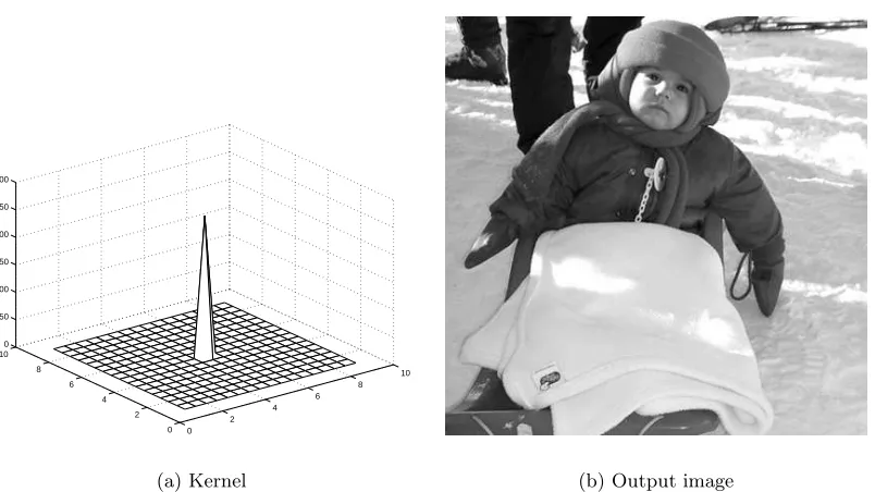
Real-time video rate of 30fps was achieved, demonstrating the effectiveness of the algo-rithm. Images taken with kernels encoding various types of filter are shown as examples below. For the test, kernels similar to those used in the software simulations of figures 3.5 to 3.8 were used on a poster filmed by the camera while the output is acquired in real time. Low-pass filters are shown along with the original image in figure 4.4. The granularity of the unfiltered image (a) is an artifact of the printed image used as a target. It helps to show the smoothing that occurs when flat or Gaussian kernels are applied: the granularity disappears, leaving a smooth background instead.
(a) Original image (b) Flat kernel
[image:49.612.123.530.147.585.2](c) Gaussianσ= 1.5 pixels (d) Gaussianσ= 2.5 pixels
(a) Gain with no distortion (b) Gain inducing saturation
Current-Mode Computational
Imager
5.1
Introduction
Several version of the convolution chip were designed, based on different principles for imple-menting the analog arithmetic operators (adders, multipliers, memory cells, etc.) necessary for calculating the convolution. In the first version, the charge-mode convolution chip, a current-based pixel array was implemented. The arithmetic operators were relying on trans-fer of charges to create voltage levels proportional to the operation result. For example, accumulation was achieved by flowing a current into a capacitor for an equal period for each input. The second version, presented in this chapter, manipulates current flows for the calculations.
The charge-mode convolution chip was fabricated and tested. It gave encouraging results for the computation but also pointed out some issues that needed to be addressed to improve the image quality and to develop a seamless interaction between the entire pixel matrix and the convolution core.
Figure 5.1: Signal flow block diagram
accommodate a full-imager convolution) and to test another approach that had shown encouraging results in simulations.
The purpose of this second generation chip was twofold. First, to demonstrate the ease or arraying the various elements so that the entire imager could be scanned at every frame and the convolution performed in a semi-parallel fashion. Second, to integrate a new convolution accumulation algorithm, saving space on chip and improving the accuracy of the calculations.
This chapter goes through the architecture of the convolution chip by following the natural flow of information. Following the diagram of figure 5.1, it starts with the pixel capturing the visual information all the way through the computing elements, to the final result of the convolution.
5.2
Imager
The imaging part of the chip is made of two entities: the pixel matrix containing the photo-sensitive elements and the pixel readout circuits, whose task is to transfer and transform the information for the pixels to the processing unit in an acceptable format.
Several types of pixel designs were studied, and two of them were implemented on dif-ferent chips. A current-mode pixel was used in the first designs to minimize the complexity of the downstream processing. Because current-based pixel designs are prone to large fixed pattern column noise [56], a mode conventional voltage-mode pixel was used in the later designs. Thanks to a voltage to current converter added in the readout stage, the current interface with the downstream processing remains unchanged.
M1
Column Column Chip pad
Icol_ref Icol_ref Icol_ref
(a) Self-biased current sources
Read pix
Ipix
(b) Current mode pixel
Figure 5.2: Column in the current-mode imager
be provided to the low impedance load of the convolution circuit. The current type pixel already provides the proper type of signal so the only additional functions needed aim at selecting the right columns that will be processed while scaling the currents to the expected range. The voltage type requires an additional conversion so the computation blocks receive a well-defined current flow. Fixed pattern noise reduction is also performed on the fly at that level.
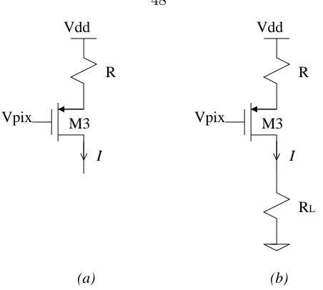
Both options, along with the corresponding readout methodology, are described in this section. Emphasis is, however, placed on the voltage mode pixel paired with a voltage to current converter which was chosen for the final design.
5.2.1 Pixel implementation
5.2.1.1 Current mode pixel
The transformation from light shining onto the pixel array to currents is a three-step process. First, the cell is reset so all potentials are initialized to a known value. Then, as light shines on the photodiode, the current source in the pixel gets biased and allows more current to flow through. And finally, the column is connected to a load where the difference between the reference current and the one flowing into the pixel is read.
Reset. Although it initiates the sequence, the reset is actually done last so the integration phase can benefit from the time needed to access the entire imager to gather light. This avoids wasting time as the imager is never idle so the frame rate is maximized.
Vpix rst =Vref −VDSsel−VDSrst,
whereVref is the voltage drop across the current source at the top of the column:
Vref =V dd−Vtp3 − s
2Iref
µpCox · s 1 W L 3 + s 1 W L 4 ! .
Integration The longest step of all. Light is gathered on the photodiode during the other rows’ readout as well as during the idle time between frames.
Vpix=Vpix rst− 1
C
Z T
0
idiodedt,
where idiode is the photodiode current which is a function of the light intensity, and
C is the junction capacitance of the diode added to the gate capacitance of Mpix.
Readout. The pixel transistor, biased by Vpix allows a current to flow through it. The purpose of the readout circuit will be to extract this information and process it.
Ipix= 1 2µnCox
W L
pix
Vpix−Vtnpix
2
The column is connected through a switch to a load which receives the difference between the reference current and the pixel current:
LN
Select
VLN
Vpix M
Figure 5.3: Voltage mode pixel
5.2.1.2 Voltage mode pixel
In this configuration, the current flowing down the pixel column is set by an externally biased current sink,MLN, shown in figure 5.3. However, the potential of that line is set by the selected pixel. It is this voltage, V pix that is sent to the readout circuit described in section 5.2.2.1.
The controls are identical to those of the current mode pixel, so the sequence is the same (reset, exposure, readout). Two noteworthy differences are that the reset is done directly without transit through the select transistor and instead of being tied to ground, the signal is extracted from the gate ofMpix.
Reset. The NMOS reset switch holds the photodiode voltage Vd at one threshold voltage below the power supply:
VdRST =Vdd−VtnRST.
Integration. The photodiode current generated by the energy brought by light discharges the photo-diode node:
Vd=VdRST −
1
C
Z T
0
idiodedt.
equation:
ILN = 1 2µn
W L
pix
Vd−Vpix−Vtnpix
2
,
where
ILN = 1 2µn
W L
LN
(VLN −VtnLN)
2=constant,
and
Vd =VdRST −
idiode·T
C .
The voltage read out is then:
Vpix=VdRST −
idiode·T
C −
s
ILN
1 2µn
W L
pix
⇒Vpix=VdRST −
idiode·T
C −(VLN−VtnLN)
v u u t W L LN W L pix (5.1)
5.2.2 Readout circuit
The pixel designs proposed in sections 5.2.1.1 and 5.2.1.2 differ in the type of load that they are intended to be connect to. The first design expects a low impedance interface such as that of the arithmetic circuits of the chip. (Section 5.3 shows that the input of the multiplier is a low impedance current mirror.) It can therefore be used as is, and a simple switch is all that is needed for a readout circuit.
The voltage mode implementation, on the contrary, is designed to communicate with a high impedance load which contradicts the design specifications of the downstream arith-metic circuits. To match the impedance of the two modules, a voltage to current converter interface was designed, with the added functionality of reducing the fixed pattern noise caused by physical mismatches in the pixels and columns.
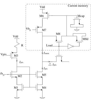
5.2.2.1 Voltage to current converter
pix
mem
pix pix
Load
Current memory
N
P
Vb
M7
I
M4 Vdd
M3 Vpix
R
M1
M2 M5
I
I
Vb
M8
M8d Mcap
I
[image:57.612.165.486.196.544.2]M6 Vdd
(a) (b) Vdd M3 Vpix R RL I Vdd M3 Vpix R I
Figure 5.5: (a) Voltage to current conversion stage and (b) with a resistive load attached
the case of the convolution chip) while drawing less power than more bulky transimpedance amplifiers. The cost of the compact circuit is a reduced linearity which is studied in this section.
AssumingM3 is in saturation (we will verify this hypothesis later),
I = 1 2µpCox
W L
3
·(VSG3 −Vtp3)2.
Let K0
3=µpCox WL3. Then, I = K03
2 (VSG3−Vtp3) 2,
⇒VSG3 =Vtp3+ s 2I K0 3 .
If we look at the voltage drop across the resistor, VR =Vdd−(Vpix+VSG3), we obtain another expression for the current I:
I = Vdd−(Vpix+VSG3)
R·I+
K0
3
−(Vdd−(Vpix+VSG3)) = 0.
Solving for I, we get:
I = 1 + (Vdd−(Vpix+VSG3))K
0
3·R+
p
1 + 2 (Vdd−(Vpix+VSG3))K30 ·R
K0
3·R2
,
or, more concisely, with the notation VR=Vdd−(Vpix+VSG3),
I = 1 +VR·K
0
3·R+
p
1 + 2VR·K30 ·R
K0
3·R2
. (5.2)
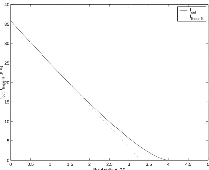
In order to plot the voltage to current conversion equation above, we use the parameters obtained from the chip fabrication:
K0
3 = 37.2µA·V
−2
× W L
3= 37.2µA·V
−2
×11..28µmµm ⇒K
0
3= 24.8×10
−6
A·V−2
PMOS transistor threshold voltage: Vtp3 = 0.96V Power supply voltage: Vdd= 5V
Resistor R: designed to beR= 65.2×10³Ω
Pixel voltage: measured to be in the range Vpix∈[0; 1.5V]
Using these parameters, we can plot equation 5.2, as shown in figure 5.6, with a linear fit of the region of interest showing the expected conversion.
Is M3 always in saturation?
0 0.5 1 1.5 2 2.5 3 3.5 4 4.5 5 0
5 10 15 20 25 30 35 40
Pixel voltage (V)
I out
, I linear fit
(
µ
A)
I
out
I
[image:60.612.113.536.195.539.2]linear fit
For a further investigation, we re-draw schematic with a load resistor RL as shown in figure 5.5(b).
M3 is in saturation ifVSD3 > VSG3−Vtp3, which is true when:
Vdd−RI−RLI > Vdd−RI−Vpix−Vtp3
⇒Vpix> RLI−Vtp3. (5.3)
The actual load for the circuit will eventually be the input of a cascode current mirror. Its resistance is determined in equation 5.6. and the current I will be at most a few microamperes. It follows that the product RLI will always be smaller than Vtp3, and
RLI −Vtp3 will always be negative. The input voltage Vpix is, on the contrary, always positive. The inequality above is therefore always true and M3 is indeed in saturation,
validating the expression of the voltage to current relation of equation 5.2. [58]
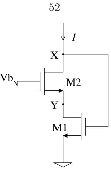
5.2.2.2 Cascode load
The V-I converter described is connected to a cascode configuration as a load. Figure 5.7 shows the cascode stage. For this system to function correctly, proper bias voltage Vb has to be provided to this cascode structure. Vb is determined by looking at the relationship between the voltage and the current of this cell and identifying the condition for saturation of the transistors.
AssumingM1 and M2 are in saturation, first look at the current to voltage relationship
inM1:
I = 1 2µnCox
W L
1
N M2 M1 Y X Vb I
Figure 5.7: Cascode readout
⇒VX =Vtn1 + s
2I µnCox WL
1
. (5.4)
The saturation of M1 and M2 is guaranteed by the setting of the bias voltage applied
to M2.
For minimal headroom consumption,
VY =VGS1−Vtn1
⇒Vbn =VGS2 + (VGS1−Vtn1)
Similarly, the voltage to current relationship in M2 is:
VGS2 =Vtn2 + s
2I µnCox WL
2
.
Substituting with equation 5.4, we obtain:
Vbn=Vtn2+
s
2I µnCox WL2
+ s
2I µnCox WL1
.
The condition of saturation of M1 and M2 is therefore:
Vbn ≥Vtn2+
s 2I µnCox
L W 1 + L W 2 . (5.5)
Figure 5.8: Cascode readout and small-signal equivalent circuit
M2 for the range of current it is intended to receive. The current is set by the conversion
from the pixel voltage and follows equation 5.2.
5.2.2.3 Resistive load of the voltage to current converter
When determining the voltage to current conversion, we assumed in equation 5.3 that the load resistance seen by the output of the converter circuit was small and we could count on the relationship RLI < Vtp3 to be true. To validate this assumption, we look at the small-signal equivalent circuit, figure 5.8, to calculate the input resistance of the cascode circuit.
i2 =i−gm2vGS2 −gmb2vBS2,
i1 =i−gm1vGS1, wherevGS2 =−ro1i1 ; vBS2 =−ro1i1 and vGS1 =vX.
vX =ro1i1+ro2i2
Substituting,
vX =ro1(i−gm1vX) +ro2(i+gm2ro1I1+gmb2ro1i1).