Int. J. Electrochem. Sci., 9 (2014) 6033 - 6042
International Journal of
ELECTROCHEMICAL
SCIENCE
www.electrochemsci.org
Characterization of Electrodeposited Ni and Ni–Mo Thin Films
by X-ray Diffraction
Masatoshi Saitou
University of the Ryukyus, Department of Mechanical Systems Engineering, 1 Senbaru Nishihara-cho Okinawa, 903-0213, Japan.
*
E-mail: [email protected]
Received: 7 July 2014 / Accepted: 4 August 2014 / Published: 25 August 2014
Electrodeposited Ni and Ni–Mo films were investigated by X-ray diffraction (XRD) and electron probe microanalysis (EPMA). Using a Williamson-Hall technique by X-ray diffraction, the Ni thin film, which shows four Bragg diffraction peaks in the XRD chart, is estimated to have a mean grain size of 30 nm. The Ni–Mo film having a Mo content of 9.6 to 10.6 at. % indicates that the Bragg peaks that exist in the XRD pattern of the Ni thin film disappear in the XRD pattern except for a broad diffraction from a (111) crystallographic plane. An atomic pair distribution function (PDF) calculated from the XRD pattern reveals that the Ni-Mo film has a long-range structural order and contains Mo as a solute atom that substitutes for a Ni atom. The electrodeposited Ni-Mo film is concluded to have a nanocrystalline characteristic comprising a Ni-Ni atomic bond and Ni-Mo atomic bond.
Keywords: Ni thin film; Ni-Mo thin film; X-ray diffraction; atomic pair distribution function; Williamson-Hall technique; nanocrystal
1. INTRODUCTION
Researchers in the field of science and technology have shown considerable interest in Ni–Mo films because these films have a wide range of applications, such as hydrogen evolution catalysis [1-2], applications requiring premium hardness [3], multilayered systems [4], and anti-corrosion treatment [5].
be close to an amorphous structure according to the X-ray analysis. On the other hand, observation with a Transmission Electron Microscope (TEM) [7] indicated that a Ni-Mo film including 30 at. % Mo comprised crystalline grains of the size of nanoscale, and was well consistent with observation by X-ray diffraction.
An atomic pair distribution function (PDF) [10-17] has been applied a quantitative study on the local structure of liquids, glasses, and disordered crystalline materials. The PDF calculated from an XRD pattern via a Fourier transformation gives the average distribution of atoms in the materials. Hence, the PDF of a Ni-Mo film can be used not only to determine the crystalline and amorphous structure, but also to study the nanostructure and the phase transition between the crystalline structure and amorphous structure. We have reported Ni-P electrodeposits having an amorphous structure [18] using the PDF calculated from the XRD pattern. However, there have been very few studies on the PDF of an electrodeposited Ni-Mo film that shows the presence of a Ni-Ni and Ni-Mo atomic bond to investigate the alloying of Mo at an atomic level.
In addition, a Williamson-Hall technique [19-21] by XRD has often been applied to determine a grain-size in a thin film. The conventional Williamson-Hall technique assuming the uniform deformation is based on the Bragg peak broadening due to the grain-size and strain in the film. Hence, several Bragg diffraction peaks are required to estimate the mean-grain size. In a modified Williamson-Hall technique considering anisotropic deformation [19], Young’s modulus, stress, and strain are dependent on the Miller indices. The Bragg diffraction broadening in the electrodeposited Ni thin film, which in this study is well described by the conventional Williamson-Hall technique, will be analyzed.
The purpose of this study is to clarify how the PDF calculated from the XRD pattern indicates the presence of Ni–Ni atomic bonds and Ni–Mo atomic bonds in the Ni–Mo film. Another goal is to determine the grain size of the Ni film using the conventional Williamson-Hall technique.
2. EXPERIMENTAL SETUP
Copper and carbon plates, each of size 30x10 mm2, were prepared to serve as cathode and anode electrodes. The two electrodes, cleaned by a wet process, were placed parallel to each other in a quiescent electrochemical cell filled with an aqueous solution including the following components (g L-1): NiSO4・7H2O, 140; KNaC4H4O6・4H2O, 100; Na2MoO4・2H2O, 0, 6.48, and 13. The solution was kept for 15 min at 355 K and filtered using a membrane with a pore size of 0.17 m.
In the experiment, a fixed current density of 10 mA was applied at a temperature of 300 K. After deposition, the film that was rinsed with distilled water and dried.
To investigate the effect of Mo on the crystallographic structure of a film, the 2.0 m thick film was electrodeposited from the solutions having sodium molybdate dihydrate concentrations of 0, 6.48, and 13 gL-1. On the other hand, films with a thickness of 24.5 m, which were electrodeposited from the solutions having sodium molybdate dehydrate concentrations of 6.48 and 13 g L-1, were prepared for the calculations of the PDF. The Mo content in the Ni–Mo film, which was necessary for the calculation of the PDF, was determined by EPMA.
3. RESULTS AND DISCUSSION 3.1. Ni thin film
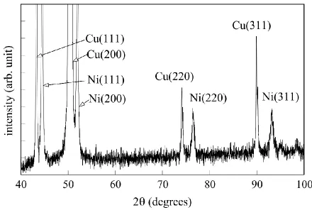
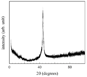
[image:3.596.76.516.363.659.2]Ni thin films electrodeposited on the copper electrode appeared mirror-like. In Fig. 1, a typical XRD chart of the nickel thin film of 2 m in thickness shows diffraction peaks of nickel comprising (111), (200), (220), and (311) planes, which peaks indicate that the Ni thin film has a polycrystalline structure.
Figure 1. XRD pattern of the 2 m thick Ni film.
In the conventional Williamson-Hall method [19-21], the line broadening of a Bragg diffraction angle B originating from a small crystalline size d and strain in a film is given by
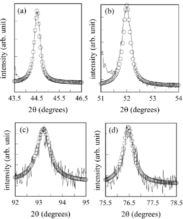
where K is the shape factor and is the X-ray wavelength. To calculate from the profile of diffraction peak, the following Gaussian function [21] G() was used as a fitting function for the diffraction peak in Fig.1,
(2) where is the fitting parameter, Lmax is the peak intensity of diffraction, Lback is the intensity of background, c is the center value of the diffraction peak. Using the integral breadth [21], the line broadening for the (hkl) plane diffraction becomes equal to . Figure 2 shows that Eq. (2) is well fitted to the diffraction peak of (111), (200), (220) and (311) planes in Fig. 1. Thus, the fitting parameter is determined.
[image:4.596.115.481.252.691.2]
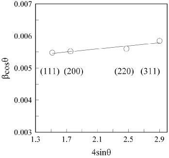
Figure 3. A Williamson-Hall plot using the line broadening coefficient calculated in Fig. 2. The y-intersect of the straight line best fitted to the line broadening coefficient yields the mean grain size of the electrodeposited nickel film using Eq. (1).
The conventional Williamson-Hall plot is shown in Fig. 3. The value of K, which is dependent on the shape of grain [22], is in a range from 0.89 to 1.3. Assuming that the grains in the Ni thin film have a sphere and the diffraction peak can be approximately represented by the Gaussian function as shown in Fig. 2, we can use K=1. All the data almost lie on the straight line, of which the y-section yields the mean grain size of 30 nm that is the same order of magnitude as that in other studies [8]. Hence, figure 3 is interpreted to show the isotropic deformation in the Ni thin film. This is because the Ni thin film comprises small grains with several crystallographic growth directions at a thickness of 2 m as shown in Fig. 1 and the deformation by the internal stress in the Ni film has a simple characteristic of tensile stress in a longitudinal direction of the nickel film. The Young’s modulus E of an electrodeposited Ni thin film is sensitive to the deposition condition [23] such as a kind of the solution, current density, and the deposition temperature. Using E=160 GPa less than the Young’s modulus of a bulk nickel, the internal stress in the Ni film is estimated to be about 0.01 GPa.
3.2 Ni-Mo film
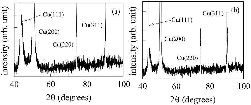
electrodeposits were mirror-like. The average Mo content in the Ni–Mo films in Figs. 4 (a) and (b) was respectively estimated to be 10.6 and 9.6 at. %, as measured by EPMA. An increase in sodium molybdate dehydrate in the solution does not necessarily increase the Mo content in the film as well as the study in Reference 8. The diffraction peaks for the Ni lattice plane (111), (200), (220), and (311) seem to disappear in both the XRD charts in the same as the past studies [6-9]. However, it is necessary to exclude the possibility that the diffraction peaks that broaden owing to Mo in the Ni-Mo film hide behind the diffraction peaks of the copper substrate. Using the XRD pattern of a much thicker Ni–Mo film, the PDF is calculated so as to investigate the crystallographic structure of the Ni– Mo film.
Figure 4. XRD patterns of the 2 m thick Ni–Mo films of for two kinds of sodium molybdate dehydrate concentration. (a) 6.48 gL-1. (b) 13 gL-1.
The calculation procedure for the PDF is as follows: The measured X-ray diffraction intensity Imeas in arbitrary units, is generally observed with XRD. The PDF is calculated from the coherent scattering intensity Icoh in electron units per atom [10]. Hence, conversion of the intensity in arbitrary units into a value expressed in electron units per atom needs the use of a normalization constant N, which in this study is calculated by the Krogh-Moe-Norman method [10–11]. In addition, the measured X-ray diffraction intensity Imeas does not directly give the coherent scattering intensity Icoh. The intensity Imeas should be corrected for polarization P, absorption A, and Compton scattering Icomp modified by the Breit-Dirac factor [10, 12],
(3)
where (4)
(5)
, (6)
[image:6.596.60.538.251.452.2]
Here, is the Bragg angle of the monochromatic crystal, is the absorption coefficient, Qmax is the upper limit, the term exp (-Q2) is an artificial damping factor (where the parameter is less than 0.01), 0 is the average atomic density, and f(Q) is the atomic scattering factor. These corrections have been discussed in the literature [10–16].
We can calculate the structure function S(Q) for the Ni–Mo film consisting of the two components, Ni and Mo, from Icoh in Eq. (3),
(8) where (9) and (10) Here, the bracket < > denotes the statistical average, ci is the atomic fraction, and fi(Q) is the atomic scattering factor that is listed in the International Tables for X-ray Crystallography [16].
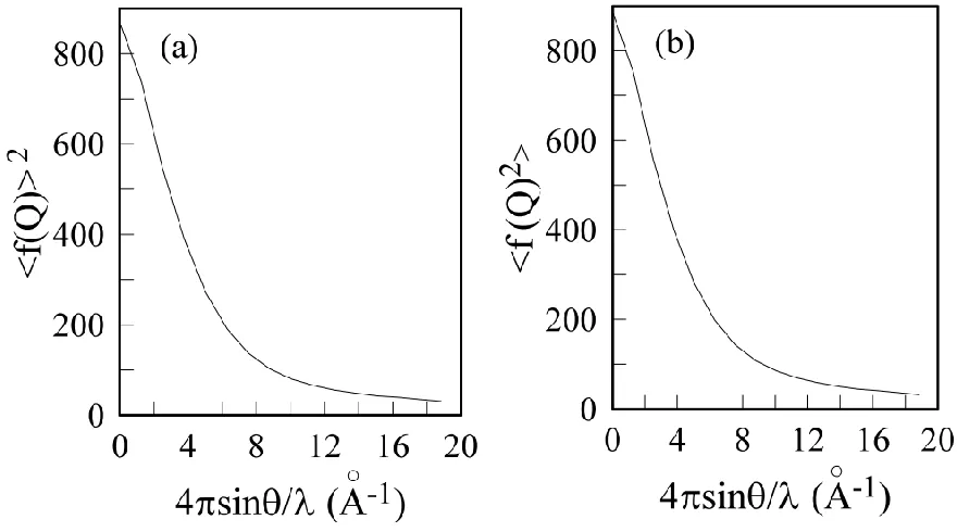
Figure 5 shows <f(Q)>2 and <f(Q)2> calculated using cMo = 0.1056 and cNi = 0.8947, which are determined by EPMA.
The PDF, g(r), can be obtained through a sine Fourier transform,
(11) where ρ(r) is the atomic density function. The PDF is a measure of the probability distribution of finding an atom at a distance r from another atom. Eq. (3) requires data from Q=0 to Q=∞, but for actual systems the integration of Eq. (3) is performed over a finite range [14].
Figure 5. Plots of <f(Q) >2 and <f(Q) 2> calculated for the calculation of PDF.
[image:7.596.76.516.417.662.2][image:8.596.118.479.130.449.2]
growth direction becomes the preferred crystallographic direction as the film thickness increases. The above-mentioned calculation procedure for the PDF yields the PDF plot shown in Fig. 7.
Figure 6. XRD pattern of the Ni–Mo film with thickness 24.5 m electrodeposited from the solution with a sodium molybdate dihydrate concentration of 6.48 gL-1.
In Fig. 7, the PDF plots of the Ni–Mo films electrodeposited from the solution with sodium molybdate dihydrate concentrations of 6.48 and 13 g L-1 are shown. The peaks in both PDF plots appear at almost the same position r. The local atomic structures of the Ni–Mo film, for example, the nearest-neighbor and second-nearest-neighbor distances between atoms, are given by the PDF. The first peak in Fig. 7 (a) is observed at r = 2.4 Å, which is almost equal to the nearest-neighbor distance in a nickel crystal [10]. The second peak at about 3.1 Å indicates a Ni–Mo atomic bond [25], which in turn indicates that the Mo solute atom is substituted for a Ni atom in the Ni–Mo film. The third peak at about 3.9 Å does not show the split peak that is observed in films having an amorphous structure. The PDF of the Ni-P film indicates a split double peak at the second peak [18], which is observed in amorphous alloys because amorphous alloys lose long-range structural orders. However, as shown in Fig. 7, the Ni-Mo film has the crystalline structure within the log-range distance.
Figure 7. PDF plots calculated from the procedure in Eq. (3)-(11). (a) PDF of the Ni–Mo film electrodeposited from the solution including a sodium molybdate dihydrate concentration of 6.48 gL-1. (b) PDF of the Ni–Mo film electrodeposited from the solution including a sodium molybdate dihydrate concentration of 13 gL-1.
4. CONCLUSIONS
Using the conventional Williamson-Hall technique, the Ni thin film is estimated to have a grain size of 30 nm. The PDF of the Ni–Mo film having a Mo content of 9.6 to 10.6 at. % indicates that the Ni-Mo film has the crystalline structure within the long-range distance, and that a solute Mo atom is substituted for a Ni atom since the Ni–Ni and Ni–Mo atomic bond are presented in the first and second peak in the PDF.
ACKNOWLEDGEMENTS
I thank Mr. K. Sakaguchi and Mr. G. Mikawa for their help with the experimental setup.
References
1. L. Mihailov, T. Spassov, I. Kanazirski, and I. Tsvetanov, J. Mater. Sci., 46 (2011) 7068. 2. D. W. Kirk, S. J. Thorpe, and H. Suzuki, Int. J. Hydrogen Energy, 22 (1997) 493. 3. R. Mousavi, K. Raeissi, and A. Saatchi, Int. J. Mod. Phys. B, 22 (2008) 3060.
4. G. Abadias, A. Debelle, A. Michel, C. Jaouen, F. Martin, and J. Pacaud, J. Appl. Phys., 107 (2010) 023515.
5. E. Chassaing E, N. Portail N, A. F. Levy, and G. Wang, J. Appl. Electrochem., 34 (2004) 1085. 6. E. Beltowaka-Lehman, A. Bigos, P. Indyka, and M. Mot, Surf. Coat. Technol., 211 (2012) 67. 7. E. Beltowaka-Lehman and P. P. Indyka, Thin Solid Films, 520 (2012) 2046.
8. M. Donten, H. Cesiulis, Z. Stojek, Electrochim. Acta, 50 (2005) 1405.
9. L. S. Sanches, S. H. Domingues, C. E. B. Marino, L. H. Mascaro, Electrochem. Commum., 6 (2004) 548.
10. Y. Waseda, The Structure of Non-Crystalline Materials, MacGraw-Hill, New-York, 1980. 11. C. N. J. Wagner, H. Ocken, and M. L. Joshi, Z. Naturforsh, 20a (1965) 325.
[image:9.596.79.518.75.255.2]
13. N. S. Gingrich, Rev. Mod. Phys., 15 (1943) 90.
14. R. Kaplow, S. L. Strong, and B. L. Averbach, Phys. Rev. A, 138 (1965) 1336. 15. C. N. J. Wagner, J. Non-Cryst. Solids, 31 (1978) 1.
16. C. H. Macgillavry and G. D. Rieck, International Tables for X-ray Crystallography Vol. 3, D. Reidel Publishing Company, Dordrech, 1985.
17. S. J. L. Billinge, Z. Kristallogr., 219 (2004) 117.
18. M. Saitou, Y. Okudaira, and W. Oshikawa, J. Electrochem. Soc., 150 (2003) C140. 19. M. Birkholz, Thin Film Analysis by X-Ray Scattering, Wiley-VCH, Weinheim, 2006. 20. G. K. Williamson and W. H. Hall, Acta Metall., 1 (1953) 22.
21. V. Biju, N. Sugathan, V. Vrinda, and S. L. Salini, J. Mater. Sci., 43 (2008) 1175. 22. J. I. Langford and A. J. C. Wilson, J. Appl. Cryst., 11 (1978) 102.
23. J. K. Luoa, A. J. Flewitta, S. M. Spearingb, N. A. Flecka, W. I. Milne, Materials Lett. 58 (2004) 2306.
24. M. H. Allahyarzadech, R. Roozbehani, and A. Ashrafi, Electrochim. Acta, 56 (2011) 10210. 25. Q. Zhang, Z.C. Li, C. Lin, and B. X. Liu, J. Appl. Phys., 87 (2000) 4147.