This is a postprint of a paper submitted to and accepted for publication at the International Symposium on Smart Electric Distribution Systems and Technologies (EDST) in 2015 [http://dx.doi.org/10.1109/SEDST.2015.7315271] and is subject to IEEE copyright.
Harmonic-by-Harmonic Time Delay Compensation
Method for PHIL Simulation of Low Impedance
Power Systems.
Abstract-- In PHIL simulations different time delays are introduced. Although it can be reduced, there is always some time delay. As a consequence, when the device under test is part of a low impedance power system such as: microgrids, marine or aero power systems, the simulation process becomes challenging due to the poor accuracy of the results achieved by the introduction of the time delay. Therefore, in order to accurately compensate for the inherent time delay introduced in Power Hardware in the Loop (PHIL) simulations, a method based on phase-shifting the reference voltage signal harmonic-by-harmonic and phase-by-phase is proposed. In this manner the time delay compensation will not affect to the system topology and therefore the dynamic behaviour of the original system will stay as it originally was in terms of power angles and V-I phase relationships for all the harmonics processed. In this paper, an experiment where the reference voltage is altered with 5th and 7th harmonics shows that the accuracy of PHIL simulations after the application of this compensation method is greatly improved compared with traditional methods. As a result, low impedance power systems are now able to experience an accurate PHIL simulation.
Index Terms--Harmonic compensation, interface algorithm, power hardware in the loop, PHIL, real time simulation, accuracy, stability, simulation time delay, low impedance power system.
I.
I
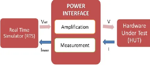
NTRODUCTIONhe first step towards the development of new testing procedures for power components was demonstrated with the development of hardware-in-the-loop simulation (HIL), which is able to merge the two traditional testing procedures (computer simulation and hardware testing) by interfacing the software simulation with the real hardware under test. Mainly controller devices are used as testing devices for HIL simulation due to the fact that they only need low power and voltage signals to be exchanged and consequently this procedure is also called controller-hardware-in-the-loop (C-HIL) simulation. Since just low level signals are exchanged between the software simulation and the hardware under test, this procedure is not valid for power components such as motors, generators or power converters that require higher levels of power to be exchanged. Hence, in order to achieve an improvement in cost, time, flexibility, risk, and accuracy of the testing methodology for these power components further development was required. The solution for HIL simulation with power components was achieved by the addition of a power interface between the software simulation and the hardware under test, as shown in Fig.1. The
power interface main task is to amplify the received signal from the real time simulation to the required power levels. Depending on the hardware under test (HUT) it can also be required to the power interface allows bidirectional transfer of energy. The method used for this type of experimentation is known as Power-HIL (P-HIL) simulation.
The main issues for PHIL are accuracy and stability of the simulation, accordingly different processes exist for the compensation of issues introduced by the power interface (time delay, noise, magnitude attenuation) affecting the accuracy or stability of the simulation. These processes are known as interface compensation methods, and will be used for an improved accuracy or/and stability during the simulation. A lead compensator block to idealize the interface to unity gain improving the accuracy of the simulation and in consequence being an interface compensation method is presented in [1]. In [2] and [3], the compensation block is a low-pass filter introduced in the feedback signal to improve the stability of the different applications, but as consequence the accuracy is affected. A multi-rating interface compensation method for the improvement of stability is presented in [4], and a comparison of the main stabilization methods used for PHIL simulation with ideal transformer method (ITM) interfaces in [5], where it is concluded that the method which presents more accurate results is the multi-rating interface.
As shown in [6] the time delay introduced by the power interface affects to the phase relationship between current and voltage and therefore to the power factor and reactive power consumption of the simulated system. Hence, if the time delay is not taken into account, it can lead to erroneous results.
E. Guillo-Sansano
University of Strathclyde [email protected]
A.J. Roscoe
University of Strathclyde [email protected]G.M. Burt
University of StrathclydeMember IEEE [email protected]
[image:1.595.314.553.213.322.2]T
This is a postprint of a paper submitted to and accepted for publication at the International Symposium on Smart Electric
Distribution Systems and Technologies (EDST) in 2015 [http://dx.doi.org/10.1109/SEDST.2015.7315271] and is subject to IEEE copyright.
For the PHIL simulation of large impedance power systems, a big inductive component can be added in the simulation (transmission line or transformer) that has the effect of lagging the current. Therefore, it can be said that compensates for the time delay, but what about the systems that have no such big inductive component? Such power systems (marine, aero or microgrid) that are known as low impedance power systems need to compensate the time delay introduced by the power interface in order to produce an accurate simulation.In [7] the average time delay is measured and calibrated by a “phase advance” applied just to the fundamental in the forward signal, in [6] a similar approach is used by phase-shifting the different frequency signals according to the time delay after a Fast Fourier Transform (FFT) has pre-processed the signals, however in this case this method has the limitation of a fixed base frequency that can impair the accuracy if the frequency changes. It could also compensate up to the 13th harmonic due to the large
computational time required to process FFTs.
In this paper a method to compensate for the time delay similar to those presented on [6,7] is presented and tested in an experimental setup. However, the reference signal will be analysed and controlled at the power interface after Discrete Fourier Transform (DFT) instead of FFT due (against the commonly held perception) to the improvement in computation efficiency and therefore an increase in the number of harmonics which can be processed. The signal will be analysed on a harmonic-by-harmonic and phase-by-phase basis, allowing the time delay to be compensated accurately by advancing the phase of the different harmonics and reconstructing the signal into time domain before its amplification, as shown in Fig. 2. With this control in the power interface, the requirement to include additional components to compensate for the time delay into the simulated power system is removed. Also an improvement on the accuracy of PHIL simulation is expected when the time-delay is compensated.
II.
T
IME DELAY COMPENSATION METHODThe time delay introduced in PHIL experiments has been habitually either ignored or avoided due to the common inductive character of large power systems, where the time delay can be simulated as part of an inductive component already existent in the system. However, low impedance power systems present a lack of big inductive components able to compensate for the introduced time delay. So, to accurately compensate for the time delay avoiding the addition of inductive components into the system, a compensation method based on DFT algorithms is proposed. For the PHIL implementation, the requirement is to measure a number of harmonics with low spectral leakage, with a variable fundamental frequency, and with a measurement update rate which matches the frame rate of the interface controller (up to or even beyond 10 kHz). While it is possible to make such measurements using an FFT process [8], it requires re-execution of the entire FFT every time a new sample is acquired. By contrast, and perhaps counter-intuitively, a bank of parallel DFT processes can be constructed to produce the same measurements with a lower computational cost per
frame, if the DFT code is carefully constructed using rolling memory buffers [9]. Use of a parallel DFT bank allows an increased number of harmonics to be processed, increasing the accuracy of the simulation. Presently, the method presented can compensate up to the 23rd harmonic in real time on the
computational platform available, at a switching frequency of 8 kHz.
In this case the reference signal to be amplified will be the voltage at the point of common coupling. So the voltage calculated in the real time simulation is transferred to the Power Amplifier control unit after an ADC and DAC respectively. Once the signal is in the control unit of the power amplifier, it is processed through the DFT transforms. The DFT algorithm used allows for a variable frequency of the processed signal, so being accurate during frequency changes. The DFT output values, in the frequency domain, will be phase-shifted harmonic by harmonic and phase by phase according to the measured loop delay, hence compensating the time delay. Then, the reconstruction of the signal into the time domain will be carried out. The reconstructed phase-shifted waveform is then introduced as reference for the PI-Resonant controller type of the Power Amplifier that finally will amplify the voltage to that of the reference and applies it to the device under test as shown in Fig 2. In this manner the time delay compensation will not affect to the system topology and therefore the dynamic behaviour of the original system will stay as it originally was in terms of power angles and V-I phase relationships for all the harmonics processed. The main limitation of this algorithm is that it is not appropriate for the accurate reproduction of fast transients, i.e. sub-cycle step-changes to the fundamental or harmonic amplitudes. The DFT window length is finite, and in this paper a 2-cycle triangular window, adaptive to fundamental frequency, is used. So, any step change in fundamental or harmonic content or voltage within the simulation will be represented as a smoothed “ramp” of the component’s amplitude/phase over 2 cycles in the PHIL environment. This is the drawback of the proposed approach. On the other hand, the benefit is that ALL the voltage-to-voltage and voltage-to-current amplitude and phase relationships for the fundamental and harmonics should be maintained accurately for quasi-steady-state operation, i.e. for all dynamic cases except the most abrupt “sub-2-cycle” step changes which will be “smoothed” over 2 cycles.
The loop delay is measured by comparing the power angle measured at the device under test terminals and the one
This is a postprint of a paper submitted to and accepted for publication at the International Symposium on Smart Electric
Distribution Systems and Technologies (EDST) in 2015 [http://dx.doi.org/10.1109/SEDST.2015.7315271] and is subject to IEEE copyright.
measured at the point of common coupling on the real time simulation. These power angles would be the same if no time delay is introduced. However, when a time delay is introduced a phase shift appears and can be accounted for.
This interface compensation method has been adopted due to its improved accuracy for performing PHIL simulations. It is able to accurately compensate the accumulated time delay of the system avoiding inserting additional components to the system that would modify the dynamic behaviour of the original system under test. This will have a great impact on the applicability of PHIL simulations, allowing low impedance power systems to be accurately tested. Voltage and current waveforms in low impedance power systems may contain significant amount of harmonics. In order to obtain accurate results the phase relationships of these harmonics is required to be preserved on both sides of the interface (simulation and hardware). The phase relationship of the fundamental voltages and currents of course relate to the power angle (power factor), but the harmonic relationships may be equally important. If the phase relationships are not maintained, then the waveform shapes (both voltage and current) on the hardware side will not match up with the waveform shapes on the simulation side. This may be a critical factor where non-linear or power-electronic devices are present either within the simulated or hardware sides of the environment.
III.
PHIL
EXPERIMENTAL SETUPFor the demonstration of the effectiveness of the compensation method presented on this paper, a simple setup for a PHIL simulation has been selected.
A procedure for performing PHIL tests similar to the one presented in [10] has been followed for this experiment. The first steps of the procedure were presented in [11] were a computer simulation with the theoretic model of the experiment was developed and its stability was tested. This time instead of using the FFT-type of compensation the DFT-type is used, the effect of this modification will not affect to the stability of the simulation.
Regarding the laboratory equipment for the demonstration of the effectiveness of the compensation method presented on this paper, the three main hardware components used for this setup are described below.
1. RTDS
The RTDS is a powerful simulation tool for performing real time power system simulations developed by RTDS Technologies. It is composed of a modular custom computing hardware with a parallel processing architecture. Depending on the application different processing and I/O cards are enclosed in each unit. These units are called racks and more than 1 may be available. The communication exchange between all cards mounted within a rack is facilitated by a common communication backplane. RTDS offer large time step and small time step simulation, although for this experiment just large time step has been used with a time step of 50µs.
The processor cards used for this experiment are the 3PC cards, each card containing three processors. The simulation blocks can be assigned to specific processors. The I/O cards required for the interaction with external hardware are assigned to different processors. In this case our input ADC is an optical analogue to digital card (OADC) with 6 input channels. The outputs are processed through the Double fiber Digital to Analogue Converter outputs card (DDAC) with 12 output channels. For the purpose of this experiment just 3 outputs and 3 inputs channels will be used.
As a voltage-type ITM interface algorithm is used for this experiment, the output signals will be the 3-phase voltage at the point of common coupling that we want to amplify, and the input signals will be the 3-phase currents measured in the HUT that will be the reference for a current source in order to be coupled to the power system.
The power system section that is simulated on the RTDS is developed in its graphical user interface, RSCAD. Fig. 3 shows the model that will be used for this experiment. As the main interest of this experiment is to demonstrate the effectiveness of the compensation method, a very simple model has been developed with a voltage source and a small impedance (ZSimulation=2.05Ω/phase). A 5% of 5th and 7th
harmonic is introduced into the system by the voltage source in order to analyse if the harmonics are properly compensated for the time delay and as consequence if the simulation is more accurate.
2. Switched mode power amplifier
The power amplifier is a back to back power converter with 3-phase and four wires rated at 15kVA developed by Triphase. This switched-mode AC/DC/AC converter is connected to the laboratory grid network in order to have power available to reproduce the reference voltage, as shown in Fig. 4. The AC/DC converter is controlled to maintain a constant DC voltage in the DC bus. The DC/AC converter is the component controlled with the signals from the RTDS, as the output of this element will try to replicate the voltage signal taken as reference. In the scenario studied in this paper it is not necessary to have bidirectional converters as the HUT will be a resistive load bank. However, the power converters of the power amplifier have bidirectional power flow capabilities, although this will only be required in cases where the HUT allows bidirectional power flow. In the configuration of the device an extra 3-phase inverter exists in order to
This is a postprint of a paper submitted to and accepted for publication at the International Symposium on Smart Electric
Distribution Systems and Technologies (EDST) in 2015 [http://dx.doi.org/10.1109/SEDST.2015.7315271] and is subject to IEEE copyright.
control the neutral current. The power amplifier switching frequency can be set from 8kHz to a maximum of 16kHz, although in this case the minimum switching frequency (8kHz) is used to allow for a longer computation time. The reference signal from the RTDS is introduced into the control by ADCs inside the power amplifier; the measurement of the response of the HUT is also measured inside of the power amplifier and sent to the RTDS with ADC devices. The fact that the measurement of the response of the HUT (currents in this case) is internal to the power amplifier has a significant drawback, as the time delay introduced in the signal will be significantly larger than if an external measurement was available. The reason being that the measurement has to wait for the next computational time step and then processed again through the DAC device before being sent to the RTDS.
This type of power interface is commonly used in PHIL applications since it is very flexible and allows improvements in the control methodology to be implemented along with its reduced cost compared with linear amplifiers; with this type of power interface the time delay compensation can have a greater impact as this interface represents a higher level of time delay.
3. Hardware Under Test (HUT)
As the scope of this paper is to demonstrate that the compensation is working properly rather than the behaviour of a specific power component, the HUT is a 3-phase variable load bank that in this case will be set to 2.2kW at 400V line-to-line. This means that the load will be of 68.5Ω/phase. Hence, meeting the stability requirements [11] where ZHUT>
ZSimulation.
IV.
L
AB EXPERIMENTR
ESULTSFor the purpose of analysing the behaviour of the time delay compensation method, a study of the phase of the different harmonics involved in this experiment (fundamental, 5th and 7th) has been carried out. The main aspect for this
investigation is the increase in phase difference between
voltage and current at the point of common coupling in the simulation.
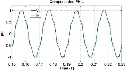
The effective phase shift introduced by the time delay on each harmonic has been examined by performing a Fourier analysis to the voltage and current waveforms produced at the software point of common coupling. Two scenarios have been studied, the first scenario consists of the power system presented in the setup without any interface compensation and the second scenario is composed of the same power system but the time delay compensation method is added. Fig. 5 shows the experiment results without the compensation method. Both the voltage and current shown are taken from the simulation at the point of common coupling. Since the load is purely resistive, the voltage and current waveforms at a node are expected to be in phase, and to contain the same harmonic composition; however it is clear that a phase shift between the fundamental voltage and current exists. Fig. 6 shows the voltage and current waveforms for the compensated PHIL simulation. In this case we can see that voltage and current at the fundamental are in phase as it was supposed to be due to the nature of the tested system.
The plot of the voltage and current waveforms is not enough to measure the impact that the compensation has on the accuracy. But more importantly it is not absolutely clear that the harmonics introduced are being compensated. Therefore, two extra measures are taken to present the results: an FFT analysis of the waveforms to study the phase of the harmonics and a total vector error (TVE) calculation of the different harmonics to measure the accuracy.
[image:4.595.39.286.52.224.2] [image:4.595.314.531.425.547.2]The Fourier analysis of the current and voltage waveforms was performed to 19 cycles of both waveforms at the same Figure 4. PHIL experimental setup.
Figure 5. Not compensated PHIL voltage and current.
[image:4.595.313.532.577.699.2]This is a postprint of a paper submitted to and accepted for publication at the International Symposium on Smart Electric
Distribution Systems and Technologies (EDST) in 2015 [http://dx.doi.org/10.1109/SEDST.2015.7315271] and is subject to IEEE copyright.
period of time in order to achieve accurate results. For the purpose of this investigation just the fundamental, 5th and 7th
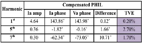
harmonics are analysed. From the Fourier analysis results of the PHIL scenario without time delay compensation presented in Table 1, it is clear that the phase shift is affecting to all the present harmonics and although the fundamental phase shift is the lower of the three it is the most significant due to its amplitude. It is also shown that the phase shift increases proportionally to the harmonic number. Table 2 shows the results of the Fourier analysis of the compensated PHIL. For this scenario, 17˚ phase compensation is introduced into the compensation algorithm. It is clear from Table 2 that the compensation is effectively phase shifting the harmonics and therefore making the simulation more accurate. Although we can see that the compensated 7th harmonic is 10˚ out of phase,
compared with the not compensated is greatly improved and as its amplitude is much less than the fundamental its effect to the fundamental is less adverse.
To measure the impact that the phase shift of the different harmonics is introducing in the waveform a similar method to the TVE defined in [12] is used. This method measures the amplitude of the vector difference between the measured vector ( ⃗ ) and the ideal ( ⃗ ) and presents the result in percentage of the ideal vector amplitude. However, to define the accuracy at the fundamental, in this case the vector difference of the harmonics is expressed as a percentage of the fundamental as:
⃗⃗ ⃗⃗
⃗⃗ (1)
TVE has been calculated for the current harmonics of phase A. Just one phase has been calculated due to the redundancy of the results caused by the balanced system. The error is measured in the current as it is the signal that experiences the time delay and therefore its harmonics are out of phase. The ideal amplitude of 5th and 7th harmonics is a 5%
of the measured fundamental current as this one is the same as the ideal calculated theoretically. The ideal phases are the phases of the voltage harmonics as the delayed signal at the point of measurement is the current.
The results of the calculated TVE for this study are presented in Table 1, where it is shown that when no compensation is introduced in the PHIL simulation the accuracy of the simulation is greatly affected. A good benchmark of acceptability of TVE for the fundamental is 1% and in this case without time delay compensation it is 29.3%, while when the compensation is introduced it is of 0.2%. Hence, in this case the TVE is proved to be inside acceptable limits, indicating a good performance of the compensation algorithm. The compensated 5th harmonic TVE is relatively
high (compared with the compensated fundamental) due to the extra 5th harmonic amplitude introduced by the power amplifier, and the same can be said of the 7th harmonic results.
However, even in this case the performance of the harmonics is notably improved compared with a non-compensated simulation. The effect that the addition of harmonic amplitude by the power interface is introducing in the PHIL simulation that affects to the accuracy of the simulation is being studied and a different control algorithm for the power interface is being developed for the improvement in this area as future work.
The results of TVE for compensated time delay PHIL simulation compared with the not compensated TVE are much smaller and therefore it can be said that the simulation accuracy has been improved.
V.
C
ONCLUSIONSWith the addition of the proposed DFT time delay compensation method into a PHIL simulation, it has been experimentally demonstrated that the phase shift introduced by different components into the simulation can be accurately compensated. So, additions of new components that are not part of the original power system are no longer required. This is a major advantage for performing PHIL simulations of low impedance power systems such as microgrids, marine or aero power systems, as consequence those systems are now able to experience an accurate PHIL simulation. The need of an inductive component into the simulation is no longer required and so the dynamic behaviour of the simulation is no longer affected. This method can be very convenient for distribution systems with an important penetration of power electronic converters, where the study of the harmonics can be essential and the accuracy of the fundamental is not enough, so an accurate harmonic analysis is also required. The accuracy of the simulation has been greatly improved by implementing the DFT time delay compensation not just to the fundamental but also to the harmonics.
The results presented in this study are in accordance with the theoretical and simulated results, and therefore confirms the performance of the time delay compensation method for PHIL simulation in low impedance networks.
R
EFERENCES[1] Ren, W., et al. “Interfacing Issues in Real-Time Digital Simulators.”
IEEE Trans. Power Delivery. 2011. vol.26, no.2, p. 1221-1230. [2] Lehfuss, F. and Lauss, G. “Power Hardware-in-the-Loop for Distributed
Generation.” 21st International Conference on Electricity Distribution.
[image:5.595.41.279.169.241.2]2011.
Table 1. Phase angle and TVE of not compensated PHIL simulation.
This is a postprint of a paper submitted to and accepted for publication at the International Symposium on Smart Electric
Distribution Systems and Technologies (EDST) in 2015 [http://dx.doi.org/10.1109/SEDST.2015.7315271] and is subject to IEEE copyright.
[3] Kotsampopoulos, P., V. Kleftakis, G. Messinis, and N. Hatziargyriou. “Design, Development and Operation of a PHIL Environment for Distributed Energy Resources.” IEEE Industrial Electronics Society.
2012. 4765 - 4770.
[4] Lehfuss, F. and Lauss, G. and Strasser, T. “Implementation of a multi-rating interface for Power-Hardware-in-the-Loop simulations.” IECON 2012 - 38th Annual Conference on IEEE Industrial Electronics Society.
2012. 4777-4782.
[5] Viehweider, A., G. Lauss, and F. Lehfub. “Stabilization of Power Hardware-in-the-Loop Simulations of Electric Energy Systems.”
Simulation Modelling Practice and Theory. 2011. vol.19, no.7, pp. 1699-1708.
[6] Ren, W., M. Steurer, and S. Woodruff. “Applying Controller and Power Hardware-in-the-Loop Simulation in designing and Prototyping Apparatuses for Future All Electric Ship.” Proc. IEEE Electric Ship Technologies Symp. 2007.
[7] Roscoe, A., A. Mackay, G. Burt, and J. McDonald. “Architecture of a Network-in-the-Loop Environment for Characterizing AC Power-System behavior.” IEEE Trans. Industrial Electronics. 2010. vol.57, no.4, pp. 1245-1253.
[8] Chang, G.W. and Chen, C.I. and Liu, Y.J. and Wu, M.C. "Measuring power system harmonics and interharmonics by an improved fast Fourier transform-based algorithm." Generation, Transmission Distribution, IET, 2008: 193-201.
[9] Roscoe, A.J., Carter, R., Cruden, A., and Burt, G.M.: "Fast-Responding Measurements of Power System Harmonics using Discrete and Fast Fourier Transforms with Low Spectral Leakage", 1st IET Renewable Power Generation Conference, Edinburgh, Scotland, 5th-8th September 2011
[10] De Jong, E., et al. European White Book on Real-Time Power Hardware in the Loop Testing. DERlab, 2012.
[11] Guillo-Sansano, E. and Roscoe, A.J. and Jones, C.E. and Burt, G.M. “A new control method for the power interface in power hardware-in-the-loop simulation to compensate for the time delay.” Power Engineering Conference (UPEC), 2014 49th International Universities. 2014. 1-5. [12] IEEE. “Standard for Synchrophasors for Power Systems, IEEE Standard