Processing and characterisation of II
–
VI ZnCdMgSe thin
fi
lm
gain structures
Brynmor E. Jones
a,⁎
,1, Peter J. Schlosser
a,1, Joel De Jesus
b, Thor A. Garcia
c, Maria C. Tamargo
c, Jennifer E. Hastie
aa
Institute of Photonics, Department of Physics, University of Strathclyde, Technology and Innovation Centre, Level 5, 99 George Street, Glasgow G1 1RD, UK
bDepartment of Physics, The Graduate Center and The City College of New York, 138th Street and Convent Avenue, New York, NY 10031, USA c
Department of Chemistry, The Graduate Center and The City College of New York, 138th Street and Convent Avenue, New York, NY 10031, USA
a b s t r a c t
a r t i c l e i n f o
Article history:
Received 3 September 2014 Received in revised form 29 June 2015 Accepted 9 July 2015
Available online 11 July 2015
Keywords:
II–VI compounds ZnCdMgSe Film Transfer Substrate Removal
Lattice-matched II–VI selenide quantum well (QW) structures grown on InP substrates can be designed for emis-sion throughout the visible spectrum. InP has, however, strong visible-light absorption, so that a method for ep-itaxial lift-off and transfer to transparent substrates is desirable for vertically-integrated devices. We have designed and grown, via molecular beam epitaxy, ZnCdSe/ZnCdMgSe multi-QW gain regions for vertical emis-sion, with the QWs positioned for resonant periodic gain. The release of the 2.7μm-thick ZnCdSe/ZnCdMgSe multi-QWfilm is achieved via selective wet etching of the substrate and buffer layers leaving only the epitaxial layers, which are subsequently transferred to transparent substrates, including glass and thermally-conductive diamond. Post-transfer properties are investigated, with power and temperature-dependent surface- and edge-emitting photoluminescence measurements demonstrating no observable strain relaxation effects or sig-nificant shift in comparison to unprocessed samples. The temperature dependent QW emission shift is found ex-perimentally to be 0.13 nm/K. Samples capillary-bonded epitaxial-side to glass exhibited a 6 nm redshift under optical pumping of up to 35 mW at 405 nm, corresponding to a 46 K temperature increase in the pumped region; whereas those bonded to diamond exhibited no shift in QW emission, and thus efficient transfer of the heat from the pumped region. Atomic force microscopy analysis of the etched surface reveals a root-mean-square rough-ness of 3.6 nm. High quality optical interfaces are required to establish a good thermal and optical contact for high power optically pumped laser applications.
© 2015 The Authors. Published by Elsevier B.V. This is an open access article under the CC BY license (http://creativecommons.org/licenses/by/4.0/).
1. Introduction
Epitaxial lift-off (ELO) and transfer of semiconductor structures from their growth substrates provides many advantages; allowing structures, grown lattice-matched on top of a high quality substrate, to be moved to substrates where the lattice mismatch would otherwise prevent high quality growth, or to those which would not be suitable for growth, e.g.flexible substrates.
The investigation into stratified or layered devices, combining monolithically grown heterostructures and non-related bulk sub-strates, is an area of active research. ELO and semiconductor transfer is afield of growing importance in research applications[1,2], in the production of thinfilm transistors[3], light emitting diodes[4], solar cells[5], sensing arrays[6], complementary metal oxide semicon-ductor circuits[7], etc.
Additional applications of ELO lie in areas where a band-gap engineered transferrable semiconductorfilm offers advantages over similar methods (e.g. the production of low noise III–V distributed Bragg reflector (DBR) mirrors with significant performance increase over the previous highest performing dielectric SiO2/Ta2O5mirror[8]).
Standard ELO in III–V and III–N semiconductor devices is performed on structures with a sacrificial layer of fast etching material underneath the device which, once removed, allows for the structure to be lifted and transferred.
For devices based on II–VI semiconductors, ELO has been demon-strated for II–VI materials grown on GaAs with a sacrificial layer of MgS[1,9]. While II–VI materials grown on GaAs allow quantum wells (QWs) with emission in the blue and into green with the incorporation of compressive strain (ZnCdSe/ZnSSe[10], ZnCdSSe/ZnSSe[11]), II– VI selenides near lattice-matched to InP provide a range of alloys with band-gaps throughout the visible spectrum[12]. For example, optically-pumped edge emitting lasers based on ZnCdSe/ZnCdMgSe QWs on InP have been demonstrated with emission from blue to red wavelengths[13].
Inherent difficulties in the II–VI selenide material systems include p-type doping of the material for electrical pumping, growing a full length ⁎ Corresponding author.
E-mail address:[email protected](B.E. Jones).
1
Present address, Fraunhofer Centre for Applied Photonics, Technology and Innovation Centre, Level 5, 99 George Street, Glasgow, G1 1RD, UK.
http://dx.doi.org/10.1016/j.tsf.2015.07.013
0040-6090/© 2015 The Authors. Published by Elsevier B.V. This is an open access article under the CC BY license (http://creativecommons.org/licenses/by/4.0/).
Contents lists available atScienceDirect
Thin Solid Films
DBR within a structure while maintaining crystal quality, and a sub-strate which absorbs throughout the visible spectrum. High quality DBRs have been achieved for material lattice-matched to GaAs through the use of superlattice structures to achieve higher refractive index con-trast while maintaining growth quality[11,14]. While this is possible for selenide material lattice-matched to InP, for optically-pumped devices the moreflexible solution, proposed here, is to transfer the structures to separate mirrors or transparent substrates.
For optically-pumped vertical gain structures such as semiconductor disk lasers (SDLs), doping is not required; however, good thermal man-agement is important for high power operation. Diamond is typically used as an intracavity heatspreader[15], or extracavity heat-sink[16]; the former requiring good optical contact as well as thermal contact be-tween the diamond and the intracavity surface of the sample, which can be achieved via capillary bonding (e.g.[17–19]). By using ELO to transfer II–VI selenide structures to transparent substrates, such as diamond, post-growth, visible spectrum vertical gain structures for use in SDL cavities can be fabricated.
An initial investigation into substrate removal of II–VI selenide struc-tures with similar designs grown lattice-matched to InP was reported by Moug et al.[20]; however, in that case the structures were adhered to glass using wax, and cracking or buckling of the II–VI material was ob-served. This was attributed to strain in the epitaxial structure, despite the support of the adhesive, preventing further transfer of the struc-tures. For simple II–VI materials grown on InP, a sacrificial MgSe layer could be used, in a similar technique to that used for GaAs[9]; however, for devices requiring layers with high-Mg content these would also be etched during the ELO process, causing structural damage. The com-plete removal of the substrate is therefore investigated as a method for achieving ELO and transfer.
In this report we demonstrate transfer of thin, II–VI selenide epitax-ialfilms, following removal of the III–V substrate and buffer layers, from a temporary glass substrate onto target substrates of diamond and glass, while maintaining the structural integrity and surface quality. Capillary bonding[21], results in good mechanical, thermal and optical contact. We foresee several applications for II–VIfilms that will benefit from the ability to place the structure on any substrate without the absorptive loss from the InP such as fast colour conversion for use in visible light communication. Building on previous reports of basic conversion of GaInN blue light emitting diodes to green, yellow and red[22], we are investigating the advantages of II–VI selenide colour conversionfilms for fast modulation speeds.
2. Experimental details
2.1. Device design and growth for vertical gain structures
The II–VI structures were grown by molecular beam epitaxy (MBE) in a Riber 2300 system, which includes both III–V and II–VI growth chambers connected by ultra-high vacuum transfer modules. Prior to growing the II–VI structure, a buffer layer of InGaAs is grown on the sub-strate to increase crystal quality, and then, following transfer to the II–VI chamber, growth of a thin low temperature (170 °C) ZnCdSe buffer layer for a better III–V/II–VI interface[23]. Crystal quality is monitored throughout the growth by reflection high-energy electron diffraction. MBE growth conditions for the II–VI materials were a substrate temper-ature of 270 °C and a Se to group IIflux ratio of approximately 6. Further details on the growth are reported elsewhere[24].
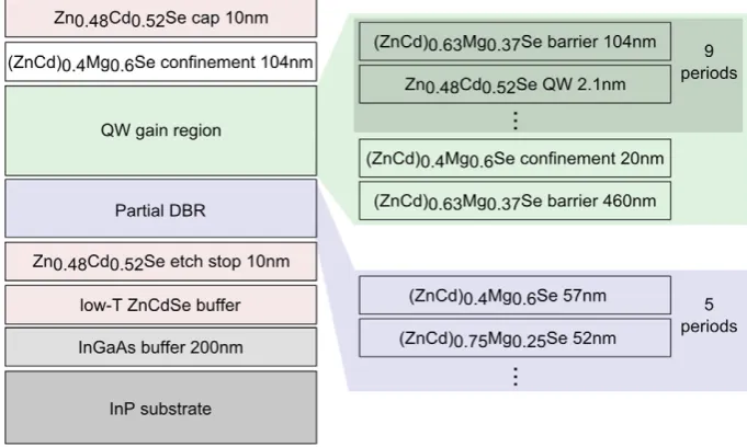
The design grown for this work, as shown inFig. 1, is a vertical gain structure with partial DBR for use within an SDL configuration.
The structure comprises 9 Zn0.48Cd0.52Se QWs designed for emission
at 550 nm, with relative positions set for resonant periodic gain[25]. All ZnCdMgSe quaternaries are grown by varying the Zn/Cd ratio for lattice-matching with InP, calibrated through X-ray diffraction (XRD) rocking curves. The pump-absorbing barriers and carrier confinement layers are ZnCdMgSe with Mg fractions of 37% and 60% respectively (band-gaps of 2.7 eV and 3.0 eV). Grown prior to the gain region, the partial DBR defines the placement of the antinodes of the electricfield standing wave with respect to the QWs and consists of alternating ZnCdMgSe layers of 25% and 60% Mg fraction, for a refractive index contrast of 0.29. The maximum refractive index contrast that may be achieved is limited by the fact that higher Mg fractions can lead to the formation of rock-salt domains[26]. Growth of alternating layers with different Mg content was achieved by changing cell temperatures between each layer. At either end of the structure are capping layers of ZnCdSe to pre-vent oxidation of the Mg containing layers; the bottom cap performing the additional function of an etch-stop. ZnCdSe absorbs at the QW emis-sion wavelength, so the cap thickness is limited to 10 nm to minimise loss while still offering protection. A scanning electron microscope (SEM) image of the cleaved edge of the un-etched structure is shown inFig. 2, the partial DBR layers and quantum wells are clearly visible.
[image:2.595.130.471.523.727.2]XRD rocking curves are used to characterise the material lattice-matching and structure strain, shown inFig. 3. The curve shows good quality growth with all peaks close to the central peak of InP, and mate-rial mismatch of no more than 0.15%.
2.2. Epitaxial lift-off and transfer
The II–VI sample is transferred by entirely removing both the InP substrate and the InGaAs buffer layer, following Moug et al.[20]. Poly-ethylene glycol (PEG), an easily removable water soluble wax with a melting point of 60 °C, is used to adhere the epi-side of the sample to a temporary glass substrate, both to protect the surface and to provide structural support during the processing. The InP substrate is mechani-cally polished to a thickness of the order of 100μm using SiC paper with a grit of 1200. The substrate of the sample is then etched with a solution of HCl:H3PO4(3:1), which does not etch the InGaAs buffer layer.
The InP/HCl:H3PO4reaction produces gaseous PH3, with an etch rate
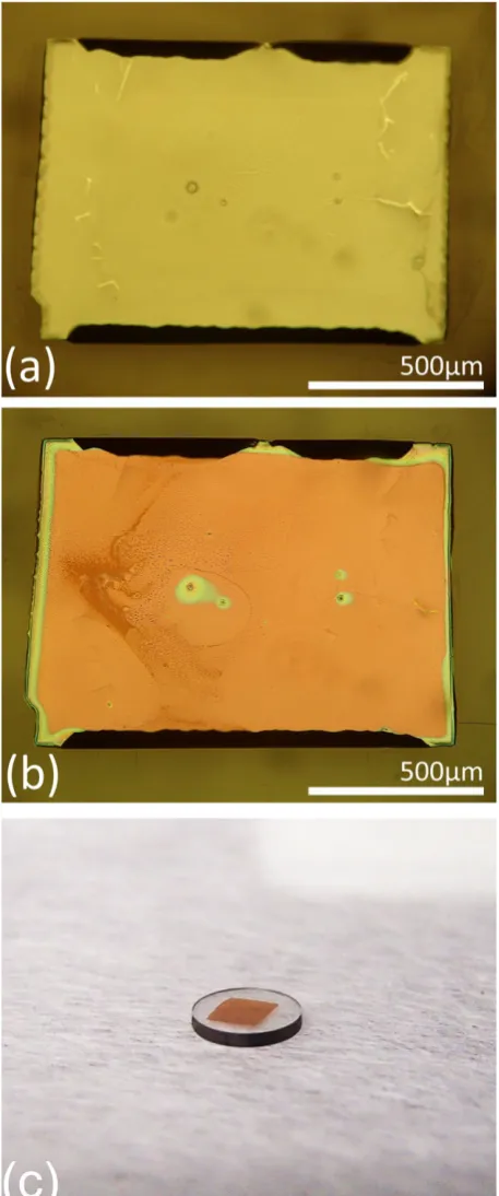
of 6.6μm/min. After an etch time of approx. 15 min no further gas bub-bles are produced, indicating that all of the InP substrate has been re-moved.Fig. 4(a) shows a microscope image of a sample etched to the InGaAs layer. Of note at this stage is the silver colour of this surface, which is easily discernible from the dark InP. The etch selectivity of the solution with InGaAs allows for the sample to remain in the acid until complete substrate removal. The InGaAs buffer is then etched using H3PO4:H2O2:H2O (1:1:6) which has a high etch selectivity for
the InGaAs/ZnCdSe interface (68:1) with an etch rate of 22.5 nm/s [20]for InGaAs. The sample changes colour over the course of the
etch, through red to a translucent yellow–orange (depending on struc-ture reflectivity and transmission characteristics) indicating that the InGaAs is fully removed (seeFig. 4(b)). Etch time is 15 seconds for com-plete InGaAs removal.
[image:3.595.313.542.53.601.2]Once the InGaAs is removed, the only remaining material still at-tached to the glass with the PEG is the II–VI epi-layer. The wax dissolves quickly when the sample is submerged in hot water (approximately
Fig. 2.SEM of the multi-quantum well structure, with the substrate to the left of the image, and DBR layer pairs showing prominently. Quantum wells are visible in the active region to the right and the top of the structure/epi-surface is shown by the black boundary.
[image:3.595.36.283.54.218.2]Fig. 3.XRD scan of as-grown structure, showing ZnCdMgSe material mismatch of 0.15% from the central substrate peak.
[image:3.595.35.280.526.717.2]70 °C) and does not damage the epi-layer. After 1–2 min in the water the sample is released from the glass.
Once released and free-floating at the water surface, the sample is
b3μm thick, but has been observed to resist cracking under moderate curvature. It can be lifted and printed onto the target substrate via cap-illary bonding to achieve an optical quality interface. Here we bonded the samples to optically-flat glass, sapphire and diamond windows (seeFig. 4(c)).
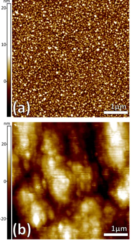
The root-mean-square (RMS) roughness of both the etched and the as-grown epitaxial surface were measured (seeFig. 5), using a Park XE-100 atomic force microscope (AFM), to be 3.6 nm and 7.0 nm respec-tively, averaged across a 5 × 5μm square of the sample. The as-grown surface corresponds to the surface profile as seen in the cross-sectional SEM image inFig. 2.
3. Results and discussion
To establish post-transfer optical characteristics, measurements of photoluminescence (PL) were recorded using a Jobin-Yvon HR460 grat-ing spectral analyser (1200 g/mm gratgrat-ing, Si detector) before and after the transfer. PL excitation was provided by a GaN diode emitting at 405 nm, focussed to a spot size of approximately 50μm radius with
power up to 42 mW, corresponding to an excitation density of approx-imately 500 W/cm2. PL collection and collimation were achieved by
using an f = 80 mm lens. The collimated light was subsequently fo-cussed into the grating spectrometer with an f = 300 mm lens. The sample is mounted on a thermo-electric cooler (TEC) with thermally conductive paste for temperature control.
PL collected at normal incidence to the structure,‘surface-PL’, shows the emission of the QWs, modulated by the optical resonances of the multilayer structure.Fig. 6(a) shows surface-PL measurements before and after processing for a sample transferred to glass and another to diamond.
Multiple peaks within the emission spectral profile are caused by the summation of multiple structuralfilters/resonances including contribu-tions from the DBR layers and the quantum well region. This profile is consistent with what would be expected within the range of only slight variation from the designed optical thicknesses. The layer thicknesses are designed so that the QWs are spacedλ/2 apart to coincide with the antinodes of the target wavelength standing wave, and the sub-cavity resonance increases the opticalfield.
[image:4.595.55.284.299.718.2]The absolute values for the processed samples cannot be accurately compared with the unprocessed sample, which includes back-reflection from the InGaAs buffer layer. What is notable, however, is
[image:4.595.315.556.310.691.2]Fig. 5.(a) AFM image of the etched II–VI surface, post-transfer, with an RMS calculated roughness of 3.6 nm. (b) AFM image of the as grown epi-layer, RMS roughness 7.0 nm.
that a distinct difference can be seen in the relative peak heights for the sample on glass. We attribute this to a pump-induced temperature in-crease being stronger for the sample bonded to glass. By observing the surface-PL of the sample on diamond with a controlled change of sam-ple temperature using the TEC, shown inFig. 6(b), it can be seen that the relative peak heights of the resonances shift due to the underlying redshift of the quantum well PL.
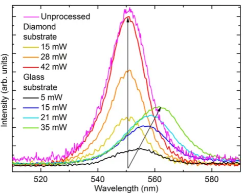
‘Edge-PL’refers to the PL emitted from the cleaved sample edges, collected using a microscope objective, so that the unmodulated QW emission may be observed. The pumped area is close to the edge of the sample to minimise PL re-absorption.Fig. 7shows the edge-PL for structures bonded to glass and diamond.
The sample on glass shows a quantum well emission redshift of 200 nm/W, compared to the sample on diamond, which shows no measurable change. This pump-induced redshift of the QW emission with pump power explains the observed relative intensity shift of the surface-PL resonance peaks for the sample on glass.
To quantify the thermal shift of the QW emission, the edge-PL for an unprocessed sample is measured atfixed low pump power with varying mount temperatures.Fig. 8shows a 0.13 nm/K redshift in the emission wavelength for the ZnCdSe/ZnCdMgSe multiple QW structure.
This compares well to the predicted thermal shift of 0.11 nm/K[27]. Thus we estimate that the pump-induced temperature increase in the gain region for the sample bonded to glass was 46 K for only 35 mW pump power.
4. Conclusions
The release of II–VI multi-quantum well thin films based on ZnCdMgSe lattice-matched to InP has been achieved by complete re-moval of the InP substrate and InGaAs buffer layer. AFM measurements demonstrate that the etched surface has low roughness suitable for cap-illary bonding to non-native substrates; in this case we have transferred the thinfilms to glass, sapphire and diamond windows.
Room temperature PL measurements show no significant shift in QW emission wavelength indicating that no strain relaxation has occurred following release from the substrate. Samples optically-contacted to diamond substrates show no shift in wavelength when optically-pumped, indicating good thermal management suitable for development of an optically pumped semiconductor disk laser[15].
The transfer of multi-QW semiconductor structures to transparent substrates allows for optical transmission configurations. This is inter-esting, e.g., for integrated II–VIfilms as colour converters or in vertical
emission external cavity lasers using transparent heat-sinks. Limitations in crystalline/interface quality and thickness due to fabrication methods, such as monolithic metalorganic vapour phase epitaxy and MBE, could be bypassed through the use of multiple stacked, separately grown semiconductor layers. This offers solutions to problems where a low refractive index contrast, i.e. for integrated DBRs, would require a high number of periods, resulting in an impractically thick structure for one single monolithic growth process. Other applications could lie in the stacking of multi-QW structures for enhanced gain (semiconduc-tor lasers) or absorption (semiconduc(semiconduc-tor saturable absorbers).
Acknowledgement
This work was supported by the Engineering and Physical Sciences Research Council (EPSRC), under Challenging Engineering Award EP/ I022791/1.
References
[1] M. Madsen, K. Takei, R. Kapadia, H. Fang, H. Ko, T. Takahashi, A.C. Ford, M.H. Lee, A. Javey, Nanoscale semiconductor‘x’on substrate‘y’—processes, devices, and applica-tions, Adv. Mater. 23 (2011) 3115–3127.
[2] A. Carlson, A.M. Bowen, Y. Huang, R.G. Nuzzo, J.A. Rogers, Transfer printing tech-niques for materials assembly and micro/nanodevice fabrication, Adv. Mater. 24 (2012) 5284–5318.
[3] E. Menard, K.J. Lee, D.Y. Khang, R.G. Nuzzo, J.A. Rogers, A printable form of silicon for high performance thinfilm transistors on plastic substrates, Appl. Phys. Lett. 84 (2004) 5398–5400.
[4] S.I. Park, Y. Xiong, R.-H. Kim, P. Elvikis, M. Meitl, D.H. Kim, J. Wu, J. Yoon, C.-J. Yu, Z. Liu, Y. Huang, K. Hwang, P. Ferreira, X. Li, K. Choquette, J.A. Rogers, Printed assem-blies of inorganic light-emitting diodes for deformable and semitransparent dis-plays, Science 325 (2009) 977–981.
[5] J. Yoon, A.J. Baca, S.-I. Park, P. Elvikis, J.B. Geddes, L. Li, R.H. Kim, J. Xiao, S. Wang, T.-H. Kim, M.J. Motala, B.Y. Ahn, E.B. Duoss, J.A. Lewis, R.G. Nuzzo, P.M. Ferreira, Y. Huang, A. Rockett, J.A. Rogers, Ultrathin silicon solar microcells for semitransparent, me-chanicallyflexible and microconcentrator module designs, Nat. Mater. 7 (2008) 907–915.
[6] Y.M. Song, Y. Xie, V. Malyarchuk, J. Xiao, I. Jung, K.-J. Choi, Z. Liu, H. Park, C. Lu, R.-H. Kim, R. Li, K.B. Crozier, Y. Huang, J. a Rogers, Digital cameras with designs inspired by the arthropod eye, Nature 497 (2013) 95–99.
[7] D.H. Kim, Y.S. Kim, J. Wu, Z. Liu, J. Song, H.S. Kim, Y.Y. Huang, K.C. Hwang, J.A. Rogers, Ultrathin silicon circuits with strain-isolation layers and mesh layouts for high-performance electronics on fabric, vinyl, leather, and paper, Adv. Mater. 21 (2009) 3703–3707.
[8] G.D. Cole, W. Zhang, M.J. Martin, J. Ye, M. Aspelmeyer, Tenfold reduction of Brownian noise in high-reflectivity optical coatings, Nat. Photonics 7 (2013) 644–650.
[9] C. Bradford, A. Currran, A. Balocchi, Epitaxial lift-off of MBE grown II–VI heterostructures using a novel MgS release layer, J. Cryst. Growth 278 (2005) 325–328.
[image:5.595.307.549.51.225.2][10] H. Jeon, J. Ding, A.V. Nurmikko, W. Xie, D.C. Grillo, M. Kobayashi, R.L. Gunshor, G.C. Hua, N. Otsuka, Blue and green diode lasers in ZnSe‐based quantum wells, Appl. Phys. Lett. 60 (1992) 2045–2047.
[image:5.595.41.279.512.700.2]Fig. 7.Quantum well emission with increasing pump power for structures transferred to diamond and glass. Arrows are included to help guide the eye and indicate wavelength shift with increasing pump power. For the sample bonded to glass, this corresponds to a spot temperature change of 46 K at 35 mW pump.
[11]C. Kruse, S.M. Ulrich, G. Alexe, E. Roventa, R. Kröger, B. Brendemühl, P. Michler, J. Gutowski, D. Hommel, Green monolithic II–VI vertical-cavity surface-emitting laser operating at room temperature, Phys. Status Solidi B 241 (2004) 731–738.
[12]M. Tamargo, A. Cavus, L. Zeng, MBE growth of lattice-matched ZnCdMgSe quater-naries and ZnCdMgSe/ZnCdSe quantum wells on InP substrates, J. Electron. Mater. 25 (1996) 259–262.
[13] L. Zeng, B. Yang, A. Cavus, W. Lin, Red–green–blue photopumped lasing from ZnCdMgSe/ZnCdSe quantum well laser structures grown on InP, Appl. Phys. Lett. 72 (1998) 3136–3138.
[14] T. Tawara, H. Yoshida, T. Yogo, Microcavities with distributed Bragg reflectors based on ZnSe/MgS superlattice grown by MOVPE, J. Cryst. Growth 221 (2000) 699–703.
[15] A.J. Kemp, G.J. Valentine, J.M. Hopkins, J.E. Hastie, S.A. Smith, S. Calvez, M.D. Dawson, D. Burns, Thermal management in vertical-external-cavity surface-emitting lasers:
finite-element analysis of a heatspreader approach, IEEE J. Quantum Electron. 41 (2005) 148–155.
[16] M. Kuznetsov, F. Hakimi, High-power (N0.5-W CW) diode-pumped vertical-external-cavity surface-emitting semiconductor lasers with circular TEM00beams, IEEE Photon. Technol. Lett. 9 (1997) 1063–1065.
[17] P. Millar, A.J. Kemp, D. Burns, Power scaling of Nd:YVO4 and Nd:GdVO4 disk lasers using synthetic diamond as a heat spreader, Opt. Lett. 34 (2009) 782–784.
[18] J. Hopkins, S. Smith, C. Jeon, H. Sun, 0.6 W CW GaInNAs vertical external-cavity sur-face emitting laser operating at 1.32μm, Electron. Lett. 40 (2004) 30–31.
[19] J.M. Hopkins, S. Calvez, A.J. Kemp, J.E. Hastie, S.A. Smith, A.J. Maclean, D. Burns, M.D. Dawson, High-power vertical external-cavity surface-emitting lasers, Phys. Status Solidi C Conf. 3 (2006) 380–385.
[20] R. Moug, A. Alfaro-Martinez, L. Peng, T. Garcia, V. Deligiannakis, A. Shen, M. Tamargo, Selective etching of InGaAs/InP substrates from II–VI multilayer heterostructures, Phys. Status. Solidi C 9 (2012) 1728–1731.
[21]Z.L. Liau, Semiconductor wafer bonding via liquid capillarity, Appl. Phys. Lett. 77 (2000) 651–653.
[22] M.A. Haase, J. Xie, T.A. Ballen, J. Zhang, B. Hao, Z.H. Yang, T.J. Miller, X. Sun, T.L. Smith, C.A. Leatherdale, II–VI semiconductor color converters for efficient green, yellow, and red light emitting diodes, Appl. Phys. Lett. 96 (2010) 231116.
[23] L. Zeng, B.X. Yang, M.C. Tamargo, E. Snoeks, L. Zhao, Quality improvements of ZnxCdyMg1−x−ySe layers grown on InP substrates by a thin ZnCdSe interfacial layer, Appl. Phys. Lett. 72 (1998) 1317–1319.
[24] J. De Jesus, T.A. Garcia, V. Kartazaev, B.E. Jones, P.J. Schlosser, S.K. Gayen, J.E. Hastie, M.C. Tamargo, Growth and characterization of ZnCdMgSe-based green light emit-ters and distributed Bragg reflectors towards II–VI based semiconductor disk lasers, Phys. Status Solidi A (2014),http://dx.doi.org/10.1002/pssa.201431439. [25]M. Raja, S. Brueck, Resonant periodic gain surface-emitting semiconductor lasers,
IEEE J. Quantum Electron. 25 (1989) 1500–1512.
[26] H.M. Wang, J.H. Chang, T. Hanada, K. Arai, T. Yao, Surface reconstruction and crystal structure of MgSefilms grown on ZnTe substrates by MBE, J. Cryst. Growth 208 (2000) 253–258.