This is a repository copy of Charged particle tracking with the Timepix ASIC. White Rose Research Online URL for this paper:
http://eprints.whiterose.ac.uk/109787/ Version: Accepted Version
Article:
Akiba, K, Artuso, M, Badman, R et al. (39 more authors) (2012) Charged particle tracking with the Timepix ASIC. Nuclear Instruments and Methods in Physics Research, Section A: Accelerators, Spectrometers, Detectors and Associated Equipment, 661 (1). pp. 31-49. ISSN 0168-9002
https://doi.org/10.1016/j.nima.2011.09.021
© 2011 Elsevier B.V. Licensed under the Creative Commons Attribution-NonCommercial-NoDerivatives 4.0 International http://creativecommons.org/licenses/by-nc-nd/4.0/
Reuse
Unless indicated otherwise, fulltext items are protected by copyright with all rights reserved. The copyright exception in section 29 of the Copyright, Designs and Patents Act 1988 allows the making of a single copy solely for the purpose of non-commercial research or private study within the limits of fair dealing. The publisher or other rights-holder may allow further reproduction and re-use of this version - refer to the White Rose Research Online record for this item. Where records identify the publisher as the copyright holder, users can verify any specific terms of use on the publisher’s website.
Takedown
If you consider content in White Rose Research Online to be in breach of UK law, please notify us by
arXiv:1103.2739v3 [physics.ins-det] 14 Jun 2011
Charged Particle Tracking with the
Timepix ASIC
Kazuyoshi Akiba4, Marina Artuso10, Ryan Badman10, Alessandra Borgia10, Richard
Bates3, Florian Bayer8, Martin van Beuzekom4, Jan Buytaert1, Enric Cabruja2, Michael
Campbell1, Paula Collins1†, Michael Crossley1,5, Raphael Dumps1, Lars Eklund3, Daniel
Esperante7, Celeste Fleta2, Abraham Gallas7, Miriam Gandelman6, Justin Garofoli10,
Marco Gersabeck1, Vladimir V. Gligorov1†, Hamish Gordon5, Erik H. M. Heijne1,4,
Veerle Heijne4, Daniel Hynds3, Malcolm John5, Alexander Leflat1,11 Lourdes Ferre Llin3,
Xavi Llopart1, Manuel Lozano2, Dima Maneuski3, Thilo Michel8, Michelle Nicol1,3, Matt
Needham9, Chris Parkes3, Giulio Pellegrini2, Richard Plackett1,3, Tuomas Poikela1,
Eduardo Rodrigues3, Graeme Stewart3, Jianchun Wang10, Zhou Xing10
1
Organisation Europ´eenne pour la Recherche Nucl´eaire, Geneva, Switzerland
2
Instituto de Microelectr´onica de Barcelona, IMB-CNM-CSIC, Barcelona, Spain
3
University of Glasgow, United Kingdom
4
Nationaal Instituut Voor Subatomaire Fysica, Amsterdam, Netherlands
5
University of Oxford, United Kingdom
6
Universidade Federal do Rio de Janeiro, Brazil
7
University of Santiago, Spain
8
Erlangen Centre of Astroparticle Physics, University of Erlangen-Nuremberg, Germany
9
School of Physics and Astronomy, University of Edinburgh, Edinburgh, United Kingdom
10
Syracuse University, Syracuse, NY 13244, USA
11
Institute of Nuclear Physics, Moscow State University (SINP MSU), Moscow, Russia
Abstract
A prototype particle tracking telescope has been constructed using Timepix and Medipix ASIC hybrid pixel assemblies as the six sensing planes. Each telescope
plane consisted of one 1.4 cm2assembly, providing a 256×256 array of 55µm square
pixels. The telescope achieved a pointing resolution of 2.3µm at the position of the
device under test. During a beam test in 2009 the telescope was used to evaluate in detail the performance of two Timepix hybrid pixel assemblies; a standard planar
300µm thick sensor, and 285µm thick double sided 3D sensor. This paper describes
a detailed charge calibration study of the pixel devices, which allows the true charge to be extracted, and reports on measurements of the charge collection characteristics
and Landau distributions. The planar sensor achieved a best resolution of 4.0±
0.1µm for angled tracks, and resolutions of between 4.4 and 11µm for perpendicular
tracks, depending on the applied bias voltage. The double sided 3D sensor, which has significantly less charge sharing, was found to have an optimal resolution of 9.0±0.1 µm for angled tracks, and a resolution of 16.0±0.2µm for perpendicular
Contents
1 Introduction 1
2 The Timepix chip 2
2.1 Description of the chip . . . 2
2.2 Use of the chip . . . 3
3 The Timepix telescope 4 4 Devices under test (DUTs) 6 4.1 Planar sensor . . . 6
4.2 3D sensor . . . 6
5 Charge calibration of DUT 7 6 Treatment of telescope data 12 6.1 Clustering algorithm . . . 12
6.1.1 Cluster finding . . . 12
6.1.2 Telescope cluster properties . . . 13
6.2 Tracking . . . 14
6.3 Telescope alignment . . . 15
6.4 Track pointing precision . . . 16
7 Analysis of the DUT 18 7.1 Description of datasets . . . 18
7.2 Establishing the orientation of the DUT in the beam . . . 21
7.3 Extracting the resolution of DUT . . . 22
8 Cluster characteristics of the sensors 22 8.1 Planar sensor Landau distributions . . . 23
8.2 Double sided 3D sensor Landau Distributions . . . 27
9 Efficiency and noise as a function of threshold 27 9.1 Planar sensor efficiency and noise results . . . 28
9.2 3D sensor efficiency results . . . 28
10 Angle dependence 30 10.1 Introduction . . . 30
10.2 Corrections due to non-linear charge sharing . . . 30
10.3 Planar sensor normal angle scans . . . 31
10.5 3D sensor normal angle scans . . . 35
11 Planar sensor bias voltage scans 37
12 Time-walk 38
13 Pulse-shape 40
14 The influence of charge digitization on the spatial resolution 42
15 Conclusions 43
1
Introduction
Pixel detectors are an attractive choice for the inner tracking regions of current and future particle physics detectors, as they provide high granularity, radiation hardness, and ease of pattern recognition. A candidate pixel ASIC which is well suited to applications at LHC, SLHC, and future forward geometry trackers with high rate and resolution requirements
is the Timepix chip characterised in this paper. The 55 µm square pixel allows single
sided modules to be built, and it can supply analogue time over threshold information in addition to the ability to associate hits to the correct bunch crossing via time stamping. The Timepix chip has not been extensively investigated for the purposes of charged par-ticle tracking, and for this reason a test experiment was performed in a charged 120 GeV pion beam at CERN’s North Area. A particle telescope was constructed using an array of Timepix and Medipix2 silicon sensor assemblies, and this was used to measure the performance of a dedicated test assembly whilst varying parameters such as silicon bias, track incident angle, and chip settings. The telescope was also used to measure the perfor-mance of a 3D sensor bonded to a Timepix chip, which represents an option for radiation hard SLHC applications. The same 3D sensor was also tested in an X-ray beam, and the results are reported in the companion paper [1]. Due to the excellent performance of the Timepix telescope, it was possible to perform a detailed investigation of the resolution, efficiency and charge sharing performance of the devices under test. This paper reports
for the first time a detailed measurement of the resolution of a 55 µm square pixel device
as a function of the angle of incident tracks to both the normal and perpendicular direc-tions with respect to the pixel columns. The charge sharing characteristics and Landau distributions obtained are discussed in detail.
Of particular interest are the plans to upgrade the LHCb silicon vertex tracker (VELO [2]) for which extensive R&D is being performed to develop a design based on pixel technology [3, 4, 5]. A pixel readout chip dedicated to the VELO application (VeloPix) will be developed based on Timepix, which will retain the advantageous geometry and analogue ToT information, but have a significantly increased readout bandwidth to cope with the higher data rates anticipated. For this reason two sections are included in this paper devoted to specific measurements relevant for LHC upgrades: the time stamping capabilities of the Timepix ASIC and the effect of reducing the number of bits available for the analogue charge measurements.
This paper reports on work carried out jointly between the Medipix2 and LHCb col-laborations.
2
The Timepix chip
2.1
Description of the chip
The design of the Timepix [6] readout chip is derived from that of the Medipix2 [7] chip which was developed for single photon counting applications. The development of the Timepix chip took place within the context of the Medipix2 collaboration at the request of and with support from the EUDet Consortium [8].
The Timepix ASIC comprises a 256×256 matrix of 55µm square pixels, each of which
contains its own analogue and digital circuitry. A globally applied shutter signal deter-mines when all pixels are active, switching between recording data and transferring it off the chip. Each pixel contains a preamplifier, a discriminator with a globally adjustable threshold, followed by mode control logic and a 14-bit pseudorandom counter with over-flow logic which stops after 11,810 counts. The threshold applied to each pixel can be individually tuned by a four-bit in-pixel trimming circuit to compensate for variations in fabrication. The three modes of operation are counting, time of arrival (ToA), and time over threshold (ToT). In counting mode the Timepix pixels behave in a similar manner to the Medipix2 pixels, incrementing the counter each time the output of the amplifier passes the threshold. In ToA mode the pixel records the time it was first hit. The counter is started when the amplifier first passes the threshold and is stopped when the shutter closes. In this mode the depth of the counter and the overflow logic limit the shutter open-ing, a particular limitation at high clock frequencies. Beyond 11,810 counts the counter saturates. In ToT mode the discriminator output is used to gate the clock to the counter, thus providing an indication of the total energy deposited. The clock and counter are used to record the time the amplifier signal is above threshold. The amplifier has been designed so that this value is linear up to 50,000 electrons and its rise and fall time can be
tuned respectively by adjusting the preamplifier and Ikrum DAC values. However, in ToT
mode the dynamic range of the measurement extends well beyond the linear range of the preamplifier output. The nominal rise time is 100 ns and the fall time 2 s. It is possible to individually program the pixels to operate in different modes from their neighbours and be read out simultaneously. The entire chip is read out after the shutter signal goes
low. Using the serial readout at 200 MHz the time to read the whole matrix is ∼5 ms.
There is a possibility of reading out the chip using a 32-bit parallel bus. In this case the
maximum clock frequency is 100 MHz and the minimum readout time∼ 300µs. Timepix
has a noise per pixel level of∼100 electrons rms and a threshold variation after tuning of
∼35 electrons rms, which leads to a minimum detectable signal on all the pixels of ∼650
electrons.
The Timepix and Medipix2 ASICs used for the telescope were bump bonded to 300µm
trimming and sensor polarity circuitry, making it equally well suited to reading out silicon sensors.
2.2
Use of the chip
In the measurements described in this paper the Timepix chips were predominantly used in ToT mode as it allowed precise track position calculations to be performed when charge was deposited in multiple pixels by the same particle. This gave the opportunity to reconstruct the impact position of the particle with a precision better than the binary
resolution, which would correspond to the 55 µm pitch divided by √12.
As the Timepix and Medipix2 chips are read out using a shutter signal in a “camera” like manner and there is no delay line or pipeline implemented in the pixels, it is not possible to use a trigger from a scintillator to read out a selected event. However, provided the hits are sparsely distributed across the chip several hundred tracks can be accumulated in one frame whilst the sensor is continuously sensitive and then read out when the shutter is closed.
Before the telescope assemblies can be operated it is necessary to set the threshold trim settings for each pixel. These bits are set to values that allow the pixels across the matrix to respond to the global threshold in a uniform way, compensating for any variation present due to inhomogenieties in fabrication or minor radiation damage. The process of setting these bits is referred to as the “threshold equalisation”.
Figure 1: Photograph of the Timepix telescope used in the testbeam.
3
The Timepix telescope
The telescope, shown in Figure 1, was constructed with four Timepix and two Medipix2 planes. This allowed the easy integration of the Device Under Test (DUT), provided complete compatibility between the readout systems and enabled an event rate of 200 Hz. The layout of the telescope together with the global coordinate frame is shown in Figure 2. Note the labels identifying each chip, which will be used on certain plots in the remainder of this paper.
The telescope consisted of six pixel planes, four Timepix and two Medipix2 separated from each other and the DUT by 78 mm. As the Medipix2 planes only provide binary in-formation, and so produce a lower resolution, they were sandwiched between the Timepix sensors; the Timepix sensors form the innermost and outermost stations of the telescope
arms. A particle passing through the sensor at an angle of tan−1( Pitch
Thickness) will always
traverse more than one pixel. This is, therefore, an approximation of the optimum an-gle of the sensor to the particle beam, at which position resolution can be improved by weighting the charge deposition in the pixels (centroiding). When the sensor is at this an-gle the centroiding calculation incorporating the ToT information from the Timepix can be used for all recorded tracks, as all the tracks will leave multi-hit clusters. Following
this logic the telescope sensors were fixed to 9◦ in both the horizontal and vertical axes
perpendicular to the beam line to optimise the spatial resolution that could be achieved by the telescope. The DUT was mounted at the centre of a symmetric arrangement of chips to further increase the resolution that could be achieved.
! ∀
!∀#∃%&∋()∗+,−)∀&
.∀/∋()∗+,−)∀&
0+1%
[image:10.595.125.510.99.333.2]#
Figure 2: A diagram of the pixel sensor assemblies within the telescope, showing the angled four Timepix and two Medipix2 sensors and the Timepix DUT with its axis of rotation. The separation of the devices shown is as measured from the centers of the chips and was enforced by the angle and the connection to the readout systems.
remotely. The stages used were supplied by PI1 and allowed a repeatability of 2 µm and
50 µrad for the translation and rotation states respectively2.
The Medipix2 and Timepix assemblies, including the DUT, were read out using USB driven systems provided by CTU [10] and the Pixelman data acquisition and control software [11]. These are the standard, portable, low bandwidth readout systems used in most Medipix applications to date. Each USB unit is attached to one chip. A signal is applied simultaneously to all the USB readout units and its rising edge triggers local shutters to individual chips. The length of the shutter is programmable in each USB unit and it was set to be the same for each assembly. It was optimised on a run by run basis to capture between 100 and 500 tracks per frame depending on beam conditions. The micro-controller in the USB unit introduces a delay between the trigger being received
and the shutter being sent of 4.0±0.5µs. As shutter periods of down to 10 ms were used
depending on the beam intensity the error on the efficiency measurement introduced by this jitter should be small. In situations where a shorter shutter is required, such as high particle flux environments, this will become a constraint on the use of the existing USB systems.
1
Physik Instrumente GmbH, D-76228 Karlsruhe 2
4
Devices under test (DUTs)
For the data taking described in this paper, two devices were investigated in the central position of the telescope; a standard planar sensor similar to the devices making up the telescope planes themselves, which was used to make a thorough investigation of the Timepix performance, and a 3D sensor, where the most interesting feature was the performance of the sensor itself in combination with the Timepix chip.
4.1
Planar sensor
The planar sensor used was one of a standard series of sensors produced by CANBERRA3
for the Medipix2 collaboration. The substrate is n-type, and the device has p+ electrodes
for hole collection. The substrate resistivity was 32 kΩcm, corresponding to 10 V full
depletion voltage for the 300 µm thick device. The leakage current of the device used in
this testbeam was less than 1 nA at 40 V applied voltage. The bump bonding assembly
was carried out at VTT4 using a Timepix chip with no inactive channels, and there is
expected to be negligible loss due to noisy pixels.
4.2
3D sensor
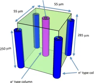
A 3D sensor has an array of n- and p-type electrode columns passing through the thickness of a silicon substrate, rather than being implanted on the substrates surface as in a planar sensor. These electrodes are realized by a combination of micro-machining techniques and standard detector technologies [12]. By using this structure it is possible to combine a standard substrate thickness of a few hundred micrometers with a lateral spacing between electrodes of a few tens of micrometers. The depletion and charge collection distances are thereby dramatically reduced, without reducing the sensitive thickness of the sensor. This implies that the device has extremely fast charge collection and a low operating voltage even after a high irradiation dose. The short collection distance and the electric field pattern in the device also reduce the amount trapping that takes place. These features
make 3D sensors potentially very radiation hard; in [13] it is shown that a 285 µm thick
double-sided 3D sensor irradiated to 10161 MeV neutron equivalents/cm2 biased at 350 V
collects 20,000 electrons. Hence, 3D sensors are a promising technology for inner layers of vertex detectors at the LHC upgrades, which require operation beyond this fluence.
The double-sided 3D sensor [14] used in the testbeam measurements described here is a modification of the traditional same-side 3D design [15]. In the same-side 3D devices the n- and p-type columns penetrate through the full thickness of the substrate, and the columns for both electrode types are etched from the same side and a handle wafer, wafer-bonded to the sensor wafer, is required in the processing. The double-sided device has the columns etched from opposite sides of the wafer for each type of column doping.
3
CANBERRA Industries, Semiconductor NV Belgium. 4
This removes the necessity to have a handling wafer and improves production yield and lowers fabrication costs.
The double-sided 3D sensor used in this beam test was designed by the University
of Glasgow and IMB-CNM and fabricated at IMB-CNM5. The geometry of the sensor,
with electrode columns passing through the thickness of the wafer from the front and
back sides, is illustrated in Figure 3. The 5 µm radius columns are produced using deep
reactive ion etching, and filled with 3 µm thickness polysilicon around the pore walls.
The columns are doped by diffusion through the polysilicon with Boron (p-type columns) or Phosphorous (n-type columns), and the inside of the columns passivated with Silica. The back surface is coated with metal for biasing and readout electrodes deposited on the front-surface. Hole and electron collecting devices were fabricated. The device used here is a hole collecting double-sided 3D n-type sensor with an n-type substrate and
p-doped columns connected to the electronic readout. The columns have a depth of 250µm,
whereas the substrate is 285±15µm thick. The region between the n- and p-type columns
depletes at only a few volts. There is a lower field region in the sensor directly above a column which requires the sensor to be biased to around 10 V to be fully active [16]. The device was solder bump-bonded by VTT to a Timepix readout chip. A lower grade Timepix readout chip was used for this R&D project with some inactive pixel columns (see later). The electrical characteristics of the double sided 3D devices measured in the laboratory are reported in [13] and [14], and the device used here had a leakage current
of 3.8µA at 20 V at room temperature.
5
Charge calibration of DUT
For the data described in this paper, the standard threshold setting and the mean THL DAC values returned by the equalisation scans described in Section 2 are shown in Table 5.
Noise Floor Noise edge Threshold Set Threshold Set
(DAC steps) (DAC steps) (DAC steps) (electrons)
D04-W0015 460 438 400 ∼1520
Table 1: Planar Sensor DUT Threshold settings. The nominal threshold in electrons is given by the difference between the set threshold and noise floor, multiplied by the expected 25.4 electrons per DAC step [17].
In order to correctly interpret the DUT data in the analyses which follow, a charge calibration of the planar sensor DUT was performed. The first aim of this charge cali-bration was to verify that the threshold indeed corresponded to the nominal value shown
5
!!∀!#∀
!!∀!#∀
∃%∀&∋()∀∗+,−#∃.∀
[image:13.595.141.458.130.411.2](%∀&∋()∀∗+,−#∃∀
Figure 3: Design of a single pixel cell in an n-type bulk double-sided 3D sensor, showing the electrode columns partially etched from the top and bottom surfaces of the sensor. The vertical scale has been compressed.
in Table 5. The second aim of the charge calibration was to be able to obtain the re-lationship between raw ToT values and charge deposited in each pixel. As explained in Section 2, the response of the Timepix is in principle a linear function of the input charge. In practice, however, there is a deviation from this behaviour, giving a global offset for each hit pixel with a value dependent on the threshold. In addition, there exists a strongly
non-linear behaviour for charges within about 3000 e− of the threshold. This behaviour
so is explained in detail here. For the 3D sensor DUT, a detailed charge calibration was not performed, however the conclusions from the calibration of the planar sensor DUT can be extrapolated to this device to infer the operational threshold.
The first part of the calibration proceeded using the testpulse function available in the Timepix and controlled via the Pixelman interface. The analog input of each pixel features
a built-in capacitor of 7.5 fF [6], and a step voltage of 1 mV therefore corresponds to 46.9 e−
injected charge [6]. The voltage of the pulse sent to the chip is generated by an analog
multiplexer6 mounted on the board, which switches the output from a reference voltage.
The precise relationship between the programmed voltage and the voltage received by the chip varies according to the USB readout system linked to the chip in question, and must be checked by measurement at the output of the multiplexer. For the planar sensor DUT the following relationship is obtained:
H =HNOM∗0.972−26.7, (1)
where H is the true test pulse height in mV, andHNOM is the nominal test pulse height.
In the ideal case, the calibration would now proceed by sending one testpulse per shutter to each pixel, and measuring the ToT and efficiency numbers for each testpulse height. In the case of the Timepix chip this is not possible, as the first testpulse sent gives a lower value than expected in the pixel array, an effect which is thought to be due to the settling time of the DACs in the setup used. This effect can be washed out by sending a large number of testpulses, however in this case the efficiency (“counting”) measurement and the ToT measurement must be done in two separate steps, as described below. In addition note that it is important to send the testpulses one at a time to individual pixels within an 8 by 8 array, with a suitable wait period between each testpulse, or the results can be misleading.
The response was first studied in counting mode, in which case no ToT information is provided by the chip. One thousand test pulses were sent per frame, and the mean number of counts per pixel measured. Three thresholds were studied, at DAC values of 380, 400, and 420, corresponding to nominal thresholds of roughly 2030, 1520, and 1020 electrons. For each pixel, a curve can be constructed of the number of counts (efficiency) as a function of the programmed testpulse voltage. Fitting an error function to the curve gives the threshold for each pixel at the 50 % efficiency point, as well as the noise of that pixel. Figure 4 shows the average efficiency of each point, with error bars indicating the RMS spread, together with the average of the 65k curves derived and fitted in this way. The programmed testpulse values are corrected to the true values using Equation 1 and
finally to electrons using the 46.9e− per mV scaling given above. In this way the average
thresholds corresponding to 420, 400, 380 DAC counts were determined to be 1030, 1550,
and 2050 e− respectively. The average pixel noise was measured to be 122 electrons, with
an RMS spread of about 3 electrons. These calibrated threshold values can be seen to be very close to the nominal ones.
The CPU time involved in performing these fits is considerable, however it is also possible make a fast derivation of the average thresholds by plotting the average efficiency
6
0 20 40 60 80 0
0.2 0.4 0.6 0.8 1 1.2
Average Efficiency
Test Pulse [mV] THL = 380
THL = 400
[image:15.595.91.533.102.311.2]THL = 420
Figure 4: Average efficiency curves obtained with the counting mode calibration. The points show the experimental data, with the applied testpulse voltage on the x axis, and the error bars indicate the RMS scatter. The curves are the averaged curves of the individual pixel fits, as described in the text.
of all pixels a function of applied testpulse voltage and fitting with a single error function. This gives results within ten electrons of the individual pixel fits, however it should be noted that in this case the measured noise is a combination of the individual pixel noise and the threshold spread, which contributes about thirty electrons in quadrature to the measured spread. These data can also be used as an indirect cross check of the testpulse
capacitor value, due to the fact that each DAC step is expected to correspond to 25.4 e−,
as reported in [17] from a measurement with sources of a different Timepix chip. The differences in thresholds between the three measurements 20 DAC steps apart can be seen to correspond very well to this expected value. Finally, note that at the lowest threshold an efficiency rise is visible at very low values of applied testpulse voltage. Due to the offset shown in Equation 1, low values of applied testpulse voltage become negative. Each testpulse generates negative and positive pulses in the pixel array, corresponding to the rising and falling edge of the testpulse. When the testpulse reverses sign, the pixels show a response corresponding to the oppositely signed edge, and this response is mirrored about the 26.7 mV offset given in Equation 1.
function”:
f(x) = ax + b− c
x−t, (2)
where a and b represent the slope and intercept of the line describing the behavior well above threshold, while t and c parameterize the non-linear behavior close to threshold [19]. In practice, electronic noise, in combination with the fact that fifty pulses are sent per shutter, smoothes the sharpness of this turn-on. We therefore fitted the measured
cal-ibration data with a convolution of the surrogate function with a Gaussian whose σ is
constrained to the one extracted for the corresponding pixel from the efficiency curves derived in counting mode. Figure 5 shows the calibration curves of the DUT for the three thresholds studied. Each data point is averaged over the 65k pixels. Near the origin of the graph one can see the edge of the response for negative pulses. It is also possible to extract the so called “minimum detectable charge”, corresponding to the intercept of
the surrogate fits with the x axis, corrected according to Equation 1 and converted into
electrons. This number is close to the threshold values quoted above, but is expected to be slightly lower due to the fact that many pulses per shutter are sent. Table 2 shows the averages of the individual pixel parameters describing the fitted surrogate functions. The parameters take into account the correction described in Equation 1.
Table 2: Summary of the surrogate function fit parameters from the “ToT” testpulse scans at three different thresholds, averaged over the individual pixel fits
THL a b c t Minimum Detectable Charge (e−)
420 0.194 34.4 195 15.3 957
400 0.201 24.8 174 25.9 1480
380 0.206 17.6 150 36.4 1980
As in the case of the counting mode measurements, the average parameters can also be obtained in a fast way by fitting the same function to the curve of the average ToT value as a function of testpulse. The numbers obtained are very close to the numbers shown in Table 2. Apart from the threshold behaviour, the main characteristic exhibited by these fits is a positive offset of the linear part of the curve, which results in a strong difference seen in the pixel spectra depending on the number of pixels per cluster. The calibration data can be used to calculate the detected charge in units of electrons, given a measured ToT, using the following “inverse surrogate function”:
qin(e−) = 46.9∗
t∗a + ToT−b +p
(b + t∗a−ToT)2 + 4∗a∗c
2∗a . (3)
which simplifies in the linear regime (above the threshold region) to:
qin(e−) = 46.9∗
ToT−b
0 200 400 600 0
20 40 60 80 100 120 140
Average ToT [/25 ns]
Test Pulse [mV] THL = 380
THL = 400
THL = 420
0 20 40 60 80
[image:17.595.91.533.103.311.2]0 5 10 15 20 25 30 35 40
Figure 5: Average test pulse response of the DUT in ToT mode, for three different thresholds. The points represent show the pulse response averaged over the 65k pixels in the DUT, as a function of the programmed testpulse voltage, with error bars indicating the RMS scatter. The curves represent averages of the individual pixel fits to the surrogate function, as described in the text. The Ikrum setting, which determines the conversion gain, was 5.
The parameters used can be those of the individual pixels, or the average fitted curves. In the latter case, there is an additional spread of less than 5%, for charge deposits around the value expected from a minimum ionising particle.
As a cross check of the studies described above, the response of the DUT to a 55Fe
source was measured, which features a 5.9 keV X-ray line, producing a charge deposition of
1640 e− in Silicon. The DUT was exposed to this source and the response measured with
the device configured in counting mode is shown in Figure 6. The main curve shows the measured efficiency curve, while the insert shows its derivative. The latter curve exhibits a clear peak at a threshold of 403 DAC counts. From this study it can be inferred that
a threshold of 400 corresponds to 1560 e−, consistent with the result obtained from the
test pulse calibration.
6
Treatment of telescope data
6.1
Clustering algorithm
6.1.1 Cluster finding
A cluster is defined as a group of adjacent hits surrounded by empty pixels. For two
hits to be considered adjacent, they must simply have a difference of 1 in their x or y
Threshold [DAC steps]
370 380 390 400 410 420 430
Mean Counts
0 0.1 0.2 0.3 0.4 0.5 0.6 0.7 0.8 0.9
Threshold [DAC steps]
370 380 390 400 410 420 430
Slope
[image:18.595.105.521.105.312.2]0 0.005 0.01 0.015 0.02 0.025 0.03 0.035
Figure 6: Average efficiency curve obtained by operating the Timepix ASIC in counting mode exposed to a 55Fe source in counting mode.
and recursively searching for adjacent hits; each time an adjacent hit is found it is added to the cluster and the search for adjacent hits repeated. The search stops when no further adjacent hits can be added to the cluster. The position of the cluster in local coordinates is assigned by making a charge weighted average of the individual pixel positions in the
row and column directions.
6.1.2 Telescope cluster properties
The distribution of ToT values in the individual pixels, and the distribution summed over the clusters, are shown in Figure 7 for a typical telescope plane. There is a small amount of noise below the Landau-like cluster peak which occurs due to interactions from
showers in the North Area pion beam; if it is required that clusters are within 100 µm
of a reconstructed track (where that device is excluded from the track fit) this noise is removed, as can be seen on the right hand plot.
In Figure 8 the total cluster charge of one, two, three, and four pixel clusters is shown
for a sample telescope plane, angled at 9◦ in the horizontal and perpendicular directions.
ToT values 0 50 100 150 200 250 300 350 400 0
0.01 0.02 0.03 0.04 0.05
0.06 Pixel TOT Values
Cluster TOT Values
ToT values 0 50 100 150 200 250 300 350 400 0
0.01 0.02 0.03 0.04 0.05
0.06 Pixel TOT Values
[image:19.595.100.531.108.310.2]Cluster TOT Values
Figure 7: The signals in individual pixels (dashed), and the signals in clusters (solid) after the clustering algorithm, shown on the left plot for a sample telescope plane. There is a small amount of noise below the Landau peak around 50. If the clusters are required to be within 100 µm of a track this noise is removed, as shown on the right hand plot. The curves are normalised to unit area.
paper it remains uncorrected in the telescope data. For the purposes of the tracking, the candidate telescope clusters have to pass only one cut, namely that the ToT is greater than 80 and less than 350 counts.
6.2
Tracking
The track reconstruction proceeds in two stages, a pattern recognition followed by a track fit. A global event cut of 5000 hits in the whole dataset is applied to reject a very small sample of saturated events. A reference sensor is chosen towards the centre
of the telescope and the global x and y of clusters in the other planes are compared
with this. The resulting distribution for all clusters is shown in Figure 9 for an adjacent plane and for the most remote plane. It can be seen that even in the most remote plane,
the track related clusters are all contained within a window of ±100 µm. Clusters are
ToT values
0 50 100 150 200 250 300 350 400
0 200 400 600 800 1000 1200
One Pixel Clusters Two Pixel Clusters Three Pixel Clusters Four Pixel Clusters
Figure 8: ToT of clusters from a sample plane in the telescope. The curves are normalised to each other for illustrative purposes. The difference in the MPV between each population is due to the positive offset introduced in each pixel by the Timepix gain curve. The relative population of one, two, three, and four pixel clusters is dependent on the device angle and is discussed in Section 7. The solid black vertical lines show the positions of the applied cuts.
x [mm]
-0.5 0 0.5
4000 5000 6000 7000 8000 9000 10000 11000 12000
Difference in global x C03-W0015
x [mm]
-0.5 0 0.5
3500 4000 4500 5000 5500 6000 6500 7000 7500
Difference in global x E05-W0015
x [mm]
-0.5 0 0.5
4000 5000 6000 7000 8000 9000 10000 11000 12000 13000
Difference in global y C03-W0015
x [mm]
-0.5 0 0.5
3500 4000 4500 5000 5500 6000 6500 7000 7500 8000
[image:20.595.121.526.105.311.2]Difference in global y E05-W0015
Figure 9: The global x and y of clusters in a given telescope plane compared to the x and y
of clusters in the reference plane. The left hand plots show these for a telescope plane next to the reference, the right hand plots show them for the telescope plane farthest from the reference.
about 100k clusters reconstructed in each plane, and approximately 64k tracks. Note that due to time alignment effects with the edges of the SPS spills some frames are empty. Typically the number of tracks reconstructed per spill was about 750.
6.3
Telescope alignment
Instead, a software alignment was used, with the only input being the rough z positions and inclinations of the planes. The coordinate system is the right handed one introduced
in Section 3: xis perpendicular to the beamline, parallel to the floor,yis perpendicular to
the beamline, perpendicular to the floor, andzis along the beamline. The free parameters
adjusted for the alignment are then (x,y,z, θx,θyand θz) whereθx,y,zare rotations about
the x,y,z axes. Physically the planes of the telescope are positioned with the sensors
away from the beam, rotated about the x and y axes by 9◦, e.g. (0,0,z,9◦,9◦,0). A
multistep offline procedure is used to refine the sensor positions. The first step roughly
aligns the planes by minimising the global x and y positions of the clusters in each
plane relative to a reference plane; allowing only x, y and θz to vary. With the sensors
now roughly aligned, tracks are fitted to the clusters, only accepting tracks with a slope
less than 0.005 radians. A χ2 is formed for each track from the sum of the residuals
divided by the expected error in each plane. The minimisation proceeds by varying the
positions of all telescope planes individually in all coordinates except z, and iterating
three times. In a final step, the procedure is repeated but the telescope planes are also
allowed to move in z. New tracks are produced and extrapolated to the DUT position.
The DUT is always excluded from the pattern recognition and the track fitting, to ensure a completely independent measurement. In the final step of the procedure the DUT is
aligned by selecting all clusters within a cut, typically 100 µm, and adjusting all 6 free
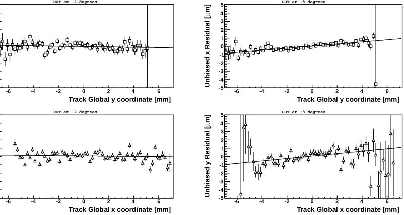
parameters of the DUT. The quality of the alignment can be probed by plotting the means of the resulting unbiased residuals at the DUT as a function of various parameters. The most sensitive parameters are found to be the orthogonal coordinate of the track to the residual plotted. The distribution is shown in Figure 10 for two sample runs with the
DUT at angles of -2◦ and 8◦: these distributions are typical. The variation of the mean
of the residual across the width of the chip is below ±1 µm; for most of the residuals
measured the effect is negligible, and for the most precise measurement angles of the
DUT the resolutions extracted in Section 7 are approximately 0.2 µm worse than what
could be achieved with an optimal alignment.
6.4
Track pointing precision
After the pattern recognition a straight line track fit is performed on the clusters selected in the telescope. For the majority of the analyses, it is required that each track has a cluster from each of the six planes. Due to the fact that the planes equipped with Medipix2 sensors are expected to have lower resolution than the Timepix planes, the track fit takes into account the errors in order to weight the clusters appropriately in the fit. The distributions of the biased residuals are studied to extract the resolution of the individual planes and the pointing resolution of the telescope at the position of the DUT. Simplifying
the expression such that the telescope planes are arranged symetrically around z = 0, it
can be shown, following the formalism developed in [20], that the predicted position of
the track at plane n is given by
ypred(n) =
X
i
Track Global y coordinate [mm]
-6 -4 -2 0 2 4 6
m]
µ
Unbiased x Residual [ -5-4
-3 -2 -1 0 1 2 3 4
5 DUT at -2 degrees
Track Global y coordinate [mm]
-6 -4 -2 0 2 4 6
m]
µ
Unbiased x Residual [ -5-4
-3 -2 -1 0 1 2 3 4
5 DUT at +8 degrees
Track Global x coordinate [mm]
-6 -4 -2 0 2 4 6
m]
µ
Unbiased y Residual [ -5-4
-3 -2 -1 0 1 2 3 4
5 DUT at -2 degrees
Track Global x coordinate [mm]
-6 -4 -2 0 2 4 6
m]
µ
Unbiased y Residual [ -5-4
-3 -2 -1 0 1 2 3 4
[image:22.595.125.526.101.315.2]5 DUT at +8 degrees
Figure 10: An illustration of the quality of the alignment for two different runs. The unbiased residual at the DUT is shown, where the DUT is excluded from the pattern recognition and from the track fitting. The variation of the mean of the residuals across the length and height of the chip is illustrated, for a run close to perpendicular, where the DUT resolution was close to 9 µm, and a run close to the optimal angle, where the DUT resolution was close to 4 µm.
where
A(zn,i) =
X
j
(zj)2+ zn·zi
(σj)2·(σi)2
X
j
1 σj2
X
j
z2
j
σ2j
, (6)
and zn is the z position at plane n, and σn the error assigned to plane n. The expected
track pointing error is then given by:
σpred(zn)=
s X
i
(σi·A(zn,i))2. (7)
The quality of the residuals in the telescope is illustrated in Figure 11, which shows
an example of the fitted residuals in the x coordinate for the six telescope planes. It can
be seen that the shapes are quite gaussian. The biased residuals extracted in each plane
inxand yfor a typical run are shown in table 3. The distribution of the biased residuals
can be used together with the formulas above to extract the expected pointing resolution at the centre of the telescope.
There is an additional error introduced by multiple scattering, although the impact is small enough that it is still acceptable to perform a straight line fit. Each station contains
Device name C03-W15 K05-W19 D09-W15 M06-W15 I02-W19 E05-W15
σx (µm) 3.3 9.4 3.9 3.8 9.3 3.2
σy (µm) 3.4 9.4 4.0 3.8 9.2 3.2
Table 3: Biased residuals measured in the telescope for a typical run. Variations between
runs are of the order of less than 0.1 µm.
thick sensor, 1.6 mm of epoxy in the PCB and a total of 87 µm of copper layers in the
PCB. The effect of this is assessed by simulating the setup, applying an extra scattering to the points, and performing a straight line fit. The result of the simulation is shown in Figure 12. The simulation gives a reasonable fit to the data, and predicts that the pointing
resolution at the position of the DUT is 2.3µm. The dominant uncertainty on this number
comes from the fact that the data are not a perfect match to the simulation. This was investigated by varying the resolution of the telescope until the simulation matched perfectly the internal and external planes. The biggest deviation induced in the pointing
resolution was 0.1µm. Additional uncertainties coming from remaning misalignments and
the lack of perfect knowledge of the material of each plane are negligible in comparison.
7
Analysis of the DUT
7.1
Description of datasets
In total about 200 runs were taken over a two week data taking period, each lasting about 50 minutes. The majority of the runs had 1000 frames, with the shutter open for 0.01 s, and a mean number of tracks of approximately 70 per frame. Nominal settings were defined, with a threshold DAC of 400 and Ikrum 5, and in general one parameter was varied at a time during each investigation. The beam intensity and the shutter open time were varied for specialised investigation of particular effects, such as alignment or time-walk. After major telescope interventions, and before taking any data set where the DUT was nominally perpendicular to the beam, a quick “angle scan” was taken. The cluster widths were analysed online in a similar way to that described in Section 7.2 to ensure that the DUT was indeed close to perpendicular. The principal datasets taken with the planar sensor:
• Angle scans: Using the motion stage the DUT was rotated about theyaxis,
caus-ing the clusters to spread in thexdirection along the pixel columns. Approximately
30 different angles were taken, concentrating on the region between zero and the
optimal angle of around 9◦, which is most relevant for LHCb, increasing to a largest
angle of 18◦, and including negative angles to investigate the symmetry around the
perpendicular point. As a final step the DUT was rotated by 45◦ about the z axis,
x position [mm]
-0.02 0 0.02
0 200 400 600 800 1000 1200
global x residuals on C03-W0015
x position [mm]
-0.02 0 0.02
0 50 100 150 200 250 300 350 400 450
global x residuals on K05-W0019
x position [mm]
-0.02 0 0.02
0 200 400 600 800 1000
global x residuals on D09-W0015
x position [mm]
-0.02 0 0.02
0 200 400 600 800 1000
global x residuals on M06-W0015
x position [mm]
-0.02 0 0.02
0 50 100 150 200 250 300 350 400 450
global x residuals on I02-W0019
x position [mm]
-0.02 0 0.02
0 200 400 600 800 1000 1200
[image:24.595.94.530.231.519.2]global x residuals on E05-W0015
Figure 11: Fitted residuals in thexcoordinate for the six telescope planes. The middle column
Telescope Plane
1 2 3 4 5 6 7
m]
µ
Biased Residuals [
[image:25.595.205.417.102.312.2]2 3 4 5 6 7 8 9 10
Figure 12: The simulation of the straight line track fit in telescope planes 1-3 (downstream of the device under test) and planes 5-7 (upstream of the device under test) shown as a solid line, and compared to the biased residuals measured in the data for the x (open circles) and y (open squares) projections.
sensor between pixels offset by one in both the column and row direction, with a constant telescope extrapolation precision.
• Shaping scans: The Ikrum parameter was varied from 5 up to 80 in order to
investigate the effect of the shaping time on the cluster landau distributions and the DUT resolution.
• Threshold scans: The threshold DAC was varied from a lowest value of around 750 electrons through to the highest possible value of around 6000 electrons. These data were used to investigate the pulse shape and the DUT efficiency. A similar scan was performed with the beam off, to investigate the noise as a function of threshold DAC.
• HV scans: The HV was varied between 5 and 200 V to investigate the cluster characteristics resolution of the DUT. These scans were performed at three different
angles: 0◦, 10◦, and 18◦.
• Time-walk: In order to investigate the time-walk the shutter open time was
de-creased to 250µs and long data runs were acquired with the Timepix in ToA mode.
Rotation Stage Angle [degrees]
-20 -15 -10 -5 0 5 10 15 20
Ratio(Width/Height)
0 0.5 1 1.5 2 2.5
Rotation Stage Angle [degrees]
-20 -15 -10 -5 0 5 10 15 20
Fraction
0 0.2 0.4 0.6 0.8
1 Fraction of 1,2,3 and 4-pixel clusters (THL=400 dac;HV=100 V)
Fraction of 1-pixel clusters Fraction of 2-pixel clusters Fraction of 3-pixel clusters Fraction of 4-pixel clusters
Figure 13: The left plot shows the distribution of the ratio of row width to column width in the 55×55µm2 planar sensor DUT; right plot shows percentage of various sizes of clusters as a function of nominal angle.
For the 3D sensor a subset of these datasets were taken, principally angle scans in the normal direction, and data at three different bias voltages.
7.2
Establishing the orientation of the DUT in the beam
Although the rotation stage can move and reproduce the angle of the DUT with very high accuracy (see Section 3), there is an uncertainty on the absolute calibration of the angle due to the uncertainty of placing the entire telescope perpendicularly in the beam line. Even though the translations and rotations of the planes relative to one another can be determined very precisely with the alignment, the overall angle with respect to the beam remains a weakly constrained parameter. For this reason a wide range of angles were scanned on both sides of the nominal perpendicular position of the DUT. Cluster characteristics independent of the tracking and alignment such as row width, column width, and fraction of 1 pixel clusters were then used to determine by symmetry arguments the position of the true perpendicular point relative to the nominal perpendicular point of the rotation stage. In order to improve the accuracy of these measurements the cluster
cleaning described in Section 6.1 was applied. Distributions of these quantities as a
function of nominal angle are shown in Figure 13. The plots show the ratio of the row width of the clusters (i.e. size in rows) to their column width (i.e. size in columns), and the fraction of various sizes of clusters as a function of angle. The plots show clear minima and maxima around the perpendicular position, and by fitting with polynomials the true position of the perpendicular can be extracted.The fits are performed in the
central region of ±5◦, and the results of the fits are shown in Table 4. The dispersion of
the beam was measured to be 0.007◦ in the direction of rotation in the stage, so adds a
Scan Minimum Angle
Cluster Size -0.205
Cluster Row Width -0.306
Fraction of 1-pixel Cluster -0.273
Ratio (Row/Column) -0.366
Table 4: The DUT angle at which each quantity is minimized.
angle of the beam relative to the nominal perpendicular point of the rotation stage was
θtrue angle =θnominal angle−0.29◦±0.06◦, (8)
and this correction is applied in subsequent plots. The error on this angle comes from the errors on the polynomial functions fitted to Figure 13, in which the errors on the individual measured points are around the permille level and therefore negligible. Essentially the entire error comes from the limited number of angles for which the measurement was performed.
7.3
Extracting the resolution of DUT
In the sections which follow the resolution of the DUT is quoted for varying conditions (track angle, HV). The resolution is always extracted in the same manner. The tracks are fitted through the telescope, as described in Sections 6.2 and Section 6.4 with the DUT excluded from the pattern recognition and from the track fit. The tracks are extrapolated to the plane of the DUT and a global residual formed between the tracks and all clusters
in the DUT. In order to investigate the resolution in x, clusters with a residual of less
than 100 µm in y are selected, and vice versa. The resulting histograms are fitted with
single Gaussians. The resolution is extracted by subtracting in quadrature the 2.3 µm
contribution from the track pointing precision. The error on the precision was estimated by dividing the datasets into two and comparing the resolution, by varying the binning of
the histograms, and by varying the cut on theyof the cluster. In addition there is slightly
larger error for the perpendicular fits, where the histograms become less Gaussian due to
the more binary nature of the resolution. It should be noted that the 0.1 µm error on the
track pointing resolution is not the dominant contribution to the error on the resolution
measurements, which are in all cases 4 µm or above.
8
Cluster characteristics of the sensors
applied. The sharp peak in the individual pixel charge as well as the importance of pixels with a low amount of charge is apparent. The track intercept point for associated clusters are shown as a function of position within the pixel cell for one, two, three, and four pixel clusters in Figure 15. The four pixel clusters, which are slightly favoured over three pixel clusters, occupy the corners of the pixel cell, with the three pixel clusters slightly inset.
8.1
Planar sensor Landau distributions
The extensive literature related to predictions of energy loss in thin silicon detector is reviewed by Bichsel in [21]. It is well known that to describe the width of the observed straggling function the effects of atomic binding must be included. Several methods have been proposed to do this. One approach is to make a n-fold convolution of the single collision cross-section derived from data on optical absorption and other measurements. An example of such an approach is discussed in detail in [21]. No analytic form for this function exists. However, in a subsequent paper Bichsel has provided tabulated data for
the cumulative probability distribution as a function of βγ which allows the expected
distribution to be generated using a Monte Carlo simulation.
An alternative approach are the so called ’mixed’ methods. In these a straggling function, obtained from a simple model of the collision spectrum, is convolved with a distribution that accounts for the atomic binding [22], [23], [24]. The simplest example of this method is to convolve a Landau distribution with a Gaussian. The resulting function is sometimes referred to as the Blunck-Leisegang function in the literature. The Landau
MPV and scale ξ are constrained by the theoretical relation
M P V(keV) =ξ[12.325 + ln ξ
I], (9)
where
ξ = 0.017825×t (µm), (10)
andtis the detector thickness in micron [21]. These formulae include density effects which
lead to an 8% increase in the MPV for highly relativistic particles compared to a MIP of
77.6 keV. The σ of the convolution Gaussian is predicted to be [22], [24]
σB = 5.72keV. (11)
Bichsel [21] has questioned the validity of this approach and shown that depending on the
assumptions made in the calculation values of σB up to a factor larger can be obtained.
To obtain good agreement between the Blunck-Leisegang and Bichsel functionsσB should
be set to 7.3 keV.
In Fig. 8.1 the charge collection distribution for all cluster sizes is compared to the results of three fits:
• A fit to the Bichsel function described above. Since the model itself has no free
parameters only the overall normalization is left free in the fit. Since the tail of
the distribution is expected to be dominated by the effect of δ-rays and not well
Number of Pixels per cluster
5 10 15 20
Number of Entries
1 10 2 10
3 10
4 10
Raw TOT counts
0 100 200 300 400
Number of Entries
0 500 1000 1500 2000 2500 3000 3500
4000 Single Pixel hits
One Pixel Clusters
Two Pixel Clusters
Three Pixel Clusters
Four Pixel Clusters
Calibrated charge [electrons]
0 20000 40000 60000
Number of Entries
0 1000 2000 3000 4000 5000 6000
7000 Single Pixel hits
One Pixel Clusters
Two Pixel Clusters
Three Pixel Clusters
[image:29.595.135.462.118.627.2]Four Pixel Clusters
x [mm]
0 0.01 0.02 0.03 0.04 0.05
y [mm]
0 0.01 0.02 0.03 0.04 0.05
ADC vs x-y position 1hit, D04-W0015
x [mm]
0 0.01 0.02 0.03 0.04 0.05
y [mm]
0 0.01 0.02 0.03 0.04 0.05
ADC vs x-y position 2hit, D04-W0015
x [mm]
0 0.01 0.02 0.03 0.04 0.05
y [mm]
0 0.01 0.02 0.03 0.04 0.05
ADC vs x-y position 3hit, D04-W0015
x [mm]
0 0.01 0.02 0.03 0.04 0.05
y [mm]
0 0.01 0.02 0.03 0.04 0.05
[image:30.595.157.459.286.580.2]ADC vs x-y position 4hit, D04-W0015
Figure 15: Cluster position distributions within the pixel cell. From left to right, the track incident point is shown in the case of associated one, two, three, and four pixel clusters.
electrons
20000
30000
40000
50000
0
5000
10000
15000
20000
25000
dataParametric fitBlunck-Leisegang function Bichsel function
Figure 16: Distribution of collected charge after charge calibration. The results of the fits described in the text are superimposed.
• A fit to a Landau convolved with a Gaussian with the parameters MPV, ξ and σB
fixed to the values given by Equation 9 - 11. As in the fit to the Bichsel function only the normalization is left free.
Table 5: Predicted and fitted Landau parameters.
Parameter Predicted value [e−] Fitted [e−]
MPV 23400 23410 ±10
ξ 1690 1820±10
σB 1580 1830±10
Table 6: Deposited charge for different cluster sizes.
.
Cluster size MPV [e−]
1 24029
2 24145
3 24214
4 24975
free. The resulting fitted parameters, compared with the predicted values from Equations 9 to 11 are displayed in Table 5.
Additional broadening effects due to electronic noise and imperfections in the gain cali-bration are small and can be ignored. To convert the theoretical estimates from keV to electrons a value of 3.62 eV for the energy necessary to create an electron-hole pair in Si [25] was used. It can be seen that though the Bichsel function describes the shape of the core of the distribution well it underestimates the MPV by around 3%. The tail of the distribution is relatively poorly described. On the other hand the Blunck-Leisegang function agrees well in terms of the MPV but underestimates the observed width of the
distribution. To describe properly theσB of the Gaussian needs to be increased from 1580
to 1830 electrons. This is in agreement with the value for σB proposed in [21].
Studies have also been performed dividing the data according to the cluster size. Fits to the parametric form described above are shown in Fig 8.1. The MPV returned by the fit are given in Table 6. It can be seen that the MPV increases slightly with increasing cluster size. This is most likely explained by the relatively high readout threshold DAC
of 1500e− which was applied and means that some charge is lost. This hypothesis is
supported by the fact that if the track information is used to select one-strip clusters where the impact point point is predicted to be close to the centre of the pixel, the
deposited charge increases from 24070 to 24479e− in better agreement with the numbers
seen for multistrip clusters.
In addition, as the cluster size increases the distribution of the deposited charge is observed to broaden. This can be explained by the fact that multi-strip clusters are more
likely to occur if a high energy δ-ray is produced.
electrons 0 20000 40000 60000 0
5000 10000 15000 20000 25000 30000 35000
One Pixel Clusters Two Pixel Clusters Three Pixel Clusters Four Pixel Clusters All Clusters combined
electrons 0 20000 40000 60000 0
0.01 0.02 0.03 0.04 0.05 0.06
0.07 One Pixel Clusters Two Pixel Clusters Three Pixel Clusters Four Pixel Clusters All Clusters combined
Figure 17: Distribution of collected charge after charge calibration for different cluster sizes. The results of fits to the parametric form described in the text are described. The right hand plot shows the same distributions but normalized to unit area, and with a zoomed x-axis.
8.2
Double sided 3D sensor Landau Distributions
The Landau distributions in the 3D sensor show a more complex shape due to the ge-ometry of the structures within the sensor. The raw ToT distributions are illustrated in Figure 8.2 for tracks at perpendicular and angled incidence. For tracks at perpendicular incidence there is a clear double peak structure, originating from tracks which pass be-tween the columns and deposit charge in the full silicon thickness, and tracks which pass through the length of a column and deposit charge in a small fraction of the thickness below. For tracks passing through the sensor at larger angles of incidence, the distri-bution represents a more uniform Landau shape. In both cases the distridistri-bution is seen to be separated from the noise floor, but closer to the threshold than in the case of the planar sensor. The detailed characteristics of the Landau distribution are discussed more extensively in the companion paper [1].
9
Efficiency and noise as a function of threshold
To measure the efficiency of the DUT, tracks were reconstructed using all six telescope planes. The intersection point of each track with the plane of the DUT was calculated, and clusters within 0.2 mm of this point were assumed to result from that track. However, if there was another track within 0.6 mm of the track in question, both tracks were ignored
to avoid associating clusters to the wrong track. The range of 0.2 mm is at least 10
Charge (ToT counts)
0 50 100 150
0 1000 2000 3000 4000 5000 6000
7000 All Clusters One Pixel Clusters Two Pixel Clusters Greater than Two Pixel Clusters
Charge (ToT counts)
0 50 100 150
0 1000 2000 3000 4000 5000
All Clusters One Pixel Clusters Two Pixel Clusters Greater than Two Pixel Clusters
Figure 18: Raw ToT distributions in the 3D double sided sensor for perpendicular tracks (left) and tracks with 10 degrees incident angle (right).
9.1
Planar sensor efficiency and noise results
The efficiency was calculated as a function of threshold for three different angles of the DUT, and is shown in Figure 19. For most thresholds the efficiency is measured to be
99.5%, with a significant drop at higher thresholds. At low threshold levels analogue
noise can cause individual pixels to be momentarily insensitive to external signals as the digital part of the pixel only responds to positive transitions across the threshold during the period when the shutter is open. Thus a high noise rate will increase the chance of the discriminator level already being above threshold when the shutter is opened, causing the overall efficiency of the device to fall.
The possibility of associating clusters to tracks incorrectly, and thereby overestimating the efficiency, was considered. The probability of associating a random cluster to a track where no real cluster existed was evaluated. It dominates the uncertainty in Figure 19 for low thresholds, but falls rapidly and becomes negligible at thresholds above 1000 electrons. The plot in Figure 19 has statistical uncertainties and this systematic uncertainty added in quadrature.
The noise was also evaluated as a function of threshold for runs taken without beam, and is plotted in Figure 20. It is high for very low thresholds, as expected, then falls to zero, or almost zero, for most thresholds under test.
9.2
3D sensor efficiency results
Threshold (electrons)
0 5000 10000
Efficiency
0.65 0.70 0.75 0.80 0.85 0.90 0.95 1.00
°
DUT angle -0.29
°
DUT angle 10
°
DUT angle 18
Threshold (electrons)
1000 2000 3000 4000 5000 6000
Mean hits per event
0 50 100 150 200 250
Threshold (electrons) 550 600 650 700 750 800 850
Mean hits per event
0 50 100 150 200 250
Figure 19: Efficiency (fraction of tracks
with associated clusters) of the 55×55µm2
[image:34.595.95.288.109.245.2]planar DUT as a function of threshold.
Figure 20: Noise (mean number of hits per event in runs without beam) as a function of threshold.
obtained per pixel, and those pixels more than four standard deviations from the mean were flagged as dead or noisy. This identified a total of 640 pixels (including the two dead columns). This map was used in the analysis and all extrapolated tracks within three pixels of a dead or noisy pixel on the 3D sensor were excluded from the analysis. Furthermore, all extrapolated tracks were required to be within the active area of the 3D sensor; the extrapolated track position was required to be seven columns from the edge of the sensor.
The double sided 3D sensor was biased to 20 V. This voltage ensures that both the inter-column region and the regions beneath the columns and the front and back-planes of the sensor are biased [14]. The Timepix chip threshold was set to approximately 1000 electrons.
Figure 21 shows the efficiency of the 3D sensor as a function of the rotation angle of the sensor. The uncertainties on the efficiencies were estimated from the mis-identification
rate. At a rotation angle of 10◦ the sensor is fully efficient, with an overall efficiency
measured as 99.8%.
As the efficiency variation across a unit pixel cell of the 3D sensor at perpendicular incidence is the main topic of the companion paper [1], only a brief description is provided here. As discussed in the introduction, the 3D sensor has a series of inactive columns, and for a perpendicular beam no charge would be collected in the centre of these columns.
However, the columns in the double sided 3D sensor have 50 µm of silicon above them
which will collect charge of around 4000 electrons when the sensor is biased at more than a few volts. As the threshold of the sensor in this study is 1000 electrons, the columns in the centre of the sensor are expected to be reasonably efficient, as seen in Figure 21, where
the efficiency in a region of 6.25µm radius around the centre columns is shown. However,