Contents lists available atScienceDirect
Diamond & Related Materials
journal homepage:www.elsevier.com/locate/diamond
Thin
fi
lm diamond membranes bonded on-demand with SOI ring resonators
Paul Hill
a,b,*, Erdan Gu
a, Martin D. Dawson
a, Michael J. Strain
aaInstitute of Photonics, University of Strathclyde, Technology and Innovation Centre, University of Strathclyde, 99 George St., Glasgow G1 1RD, United Kingdom of Great
Britain and Northern Ireland
bDiamond Science and Technology, Centre for Doctoral Training, University of Warwick, Gibbet Hill Road, Coventry CV4 7AL, United Kingdom of Great Britain and
Northern Ireland
A B S T R A C T
The hybrid integration of single-crystal (SC) diamond membranes with on-chip optical devices has the potential to service many applications, spanning non-linear optics to quantum photonics with embedded diamond colour centres. Limited dimensions of high optical quality diamond however restrict the size and number of devices that can be fabricated on a single chip, which impedes the use of diamond in large photonic integrated circuitry. Here we show the fabrication and integration of a 1μm thick SC diamond membrane with a silicon photonic device. The quality of the diamond-silicon interface is measured using SEM and optical techniques. Silicon microring resonators are measured after integration with the diamondfilm and show a low excess loss of 0.4 dB and a group index dispersion that is dependent on the mode confinement in the diamond layer.
1. Introduction
Diamond is attractive as a material for use in high-performance on-chip photonic devices. It boasts a large Raman gain (~10 cm/GW@1μ m), a wide bandgap (5.5 eV@RT), and impressive thermal properties such as its high thermal conductivity (2 × 10³Wm−1K−1) and small
thermo-optic coefficient (~10−5K−1) [1,2]. It has a large Kerr
non-linearity and also plays host to several promising defect centres. The large bandgap of diamond corresponds to a transparency spanning ul-traviolet wavelengths into the deep infrared, and its high refractive index of ~2.4 gives good optical confinement and thus enables na-noscale photonic structures. Current single crystal diamond material is only available in small mm scale pieces, making fabrication of mono-lithic large scale integrated circuits a significant challenge. To harness diamond for integrated photonic applications, a method by which thin film material can be integrated with other optical devices is required. In this work we present a hybrid integration technique based on the bonding of a flexible diamond platelet to pre-fabricated integrated photonic devices on a different material. The host devices in this work are fabricated on the silicon platform. The well-established character-istics of silicon photonic devices allow the probing of the diamond-si-licon bond interface. Nevertheless, the method is equally applicable across a wide range of material platforms. The choice of host integrated photonic platform will be dictated by the target application, for ex-ample, silicon may be used for non-linear optical applications in the telecommunications and Mid-IR bands [2-4], whilst a range of III-V
semiconductors or SiN, which are transparent in the visible and near-IR, would be compatible with coupling to diamond colour centres for quantum applications [5-8]. Integration of diamond with established photonic circuitry is limited due to the difficulty with which it is pro-cessed. Many recent efforts have been made such as by fabricating thin GaP membranes and then transferring them to bulk diamond where single mode resonators are then fabricated [8-11]. GaP presents a high refractive index, mechanically durable material, with low optical ab-sorption (2.3 eV bandgap [12]) that satisfies waveguiding criteria for some of the defect centres in diamond. Another recent approach is to use diamond resonators fabricated on a SiO2substrate with SU8
spot-size converters extending the diamond guides for end-fire injection via lensedfibre [2,4,13-15]. This approach gives a low input loss (1 dB/ facet), a waveguide propagation loss of 0.34 dB cm−1 and an index difference that gives the majority mode overlap within the diamond structure. Another method whereby suspended diamond windows are fabricated for subsequent patterning and transfer from a rigid diamond frame has been demonstrated by utilising a CVD overgrowth technique that shows very good uniformity [16,17]. Other diamond photonic devices have also been fabricated, most notably, diamond nanopillars that show optimal coupling of the pillar mode with native NV emissions [18,19] and 2D photonic crystal structures in diamond with cavity modes close to the zero phonon lines of the most promising colour centres (NV−and SiV−) [15,20-24]. Angled etching of bulk diamond chips masked by Si/SiO2 to create suspended structures such as pho-tonic crystals or microresonators have also shown great potential for
https://doi.org/10.1016/j.diamond.2018.07.020
Received 19 March 2018; Received in revised form 4 July 2018; Accepted 23 July 2018
*Corresponding author at: Institute of Photonics, University of Strathclyde, Technology and Innovation Centre, University of Strathclyde, 99 George St., Glasgow
G1 1RD, United Kingdom of Great Britain and Northern Ireland. E-mail address:paul.hill@strath.ac.uk(P. Hill).
Diamond & Related Materials 88 (2018) 215–221
Available online 26 July 2018
0925-9635/ © 2018 The Authors. Published by Elsevier B.V. This is an open access article under the CC BY license (http://creativecommons.org/licenses/BY/4.0/).
colour centre integration [25-30]. Common challenges in most of these works however are in overcoming the severe constraints on circuit in-tegration owing to the limited dimensions (~mm2) of available
elec-tronic grade diamond and also with the potential for scaling. Here we propose the fabrication of thin single-crystal diamond membranes using dry etching, that can be transferred onto established photonic circuitry using liquid mediated capillary bonding. A target thickness of diamond is chosen such that it has an increasedflexibility whilst remaining ro-bust to minimal handling during transfer. This promotes deformation of the diamond over the device it has to be bonded with. By this approach established fabrication methods can be used for large wafer-scale de-vices where the diamond is transferred afterwards as a passive com-ponent over the required devices. In this work a 1μm thick SC diamond membrane was fabricated and transferred onto Si ring resonator de-vices. Silicon was chosen as a platform for diamond integration as it provides low-loss, highly confining waveguide devices that are well understood and could be used for non-linear applications. This tech-nique can however be used with any planar waveguide technology, such as GaN which has a refractive index more closely matching that of diamond at wavelengths for NV−colour-centre emissions.
2. Device design & fabrication
The Silicon devices in this work were fabricated on a silicon on insulator (SOI) wafer with a 220 nm core layer on a 2μm buried oxide layer. The waveguides were designed to be 500 nm wide and were patterned using a 200 nm thick e-beam curable, silica-like, hydrogen silesquioxane (HSQ) epoxy. SU8 resist was used for spot size conversion tapers between the guides and external injection fibre. The ring re-sonators were designed to have a bend radius of 50μm in a racetrack geometry to give control of the cross coupling coefficient, i.e. the amount of light that will couple to the resonator from the injection waveguide, using a straight coupling section of 41.2μm [31]. Devices were prepared with both the HSQ mask in place and HSQ mask re-moved, to show the effect of mode overlap in the material stack. The devices with the cap removed, were treated using a CHF3reactive ion
etch (RIE) which etches the SiO2substrate also - thus the Si devices
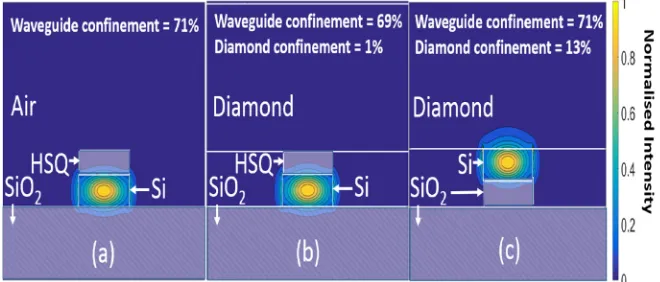
were left on a plinth of the substrate which is shown inFig. 1. Standard single mode silicon waveguides at telecommunication wavelengths have an effective index larger than that of diamond thus confining the mode more strongly to the former. Finite difference eigenmode (FDE) simulations (Fig. 1) were used to show this whilst also highlighting that an increasing thickness of diamond membrane had negligible effect on the mode overlap between the two materials. As such, the thickness of diamond was instead dictated by the requirement of membrane fl ex-ibility to promote larger areas of bonding to the target device. The confinement of the modal power was simulated for three distinct cases, in each case the fundamental transverse electric (TE) mode at a
wavelength 1.535μm was calculated. The cases were as follows, the silicon device alone with the HSQ cap; the diamond bonded to the si-licon, buffered with the HSQ cap; andfinally the diamond bonded to a device with the HSQ removed using RIE. These three cases are depicted in the mode simulations shown inFig. 1. The simulations showed that for the Silicon device with its HSQ cap present there was a 71% con-finement of the modal power within the Si waveguide. This dropped slightly when bonded with diamond to 69% and confinement to the diamond was shown to be less than 1 % of the power. For the devices where the HSQ cap had been removed before the diamond was bonded, a 71% modal power confinement to the Si was found but an increase to 13% confinement was observed within the diamond. The diamond membranes in this work were fabricated using Element 6’s commer-cially available electronic grade SC diamond chips with dimensions 4 × 4 × 0.3 mm3. The chips were laser diced and mechanically po-lished into 8 separate samples with approximate dimensions and roughness of 2 × 2 × 0.03 mm3and 2 nm r.m.s. respectively. The
dia-mond plates were cleaned in a solution of H2SO4:H2O2with a ratio of
3:1 (Piranha) to remove any organic contaminants and then thinned using an ArCl2 inductively coupled plasma (ICP) RIE [32] to 1μ m
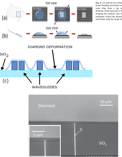
thickness at their thinnest for increasedflexibility. The diamond etch rate was approximately 65 nm/min and showed a reduction in surface roughness to < 1 nm r.m.s. as has been reported previously for this etch process [32]. Monitoring of the diamond thickness was achieved by white light optical profiling (vertical scanning interferometry). The resultant diamond profile was wedged as is common using this fabri-cation method [33], showing an approximately 4μm thickness diff er-ence across a sample length of 2 mm after polishing. Measurements taken intermediately between staged etches showed a variation of < 0.2μm in the wedge between the start and end of the thinning process. It was found that the thinner end of the diamond membrane more readily deformed over the devices with larger areas bonded than that of the thicker end. The diamondfilm was integrated with the target silicon devices by using a liquid mediated capillary bonding method. The target device was prepared with a droplet of isopropyl alcohol and the diamond brought into contact and transferred from a wetted corner of cleanroom wipe. Capillary forces as the liquid evaporates brings the membrane into close contact with the device promoting adhesion. Having been pre-thinned to a target thickness of around 1μm at its thinnest end, and with care in alignment, the diamond membrane de-forms over the devices as shown schematically inFig. 2. Nothing other than the capillary forces detailed were used in adhering the diamond to the silicon device.
3. Membrane integration with photonic devices
[image:2.595.37.367.593.734.2]To probe the quality of this interface a number of complementary techniques were used: scanning electron microscopy (SEM), analysis of
white light interference patterns, and optical transmission spectra. SEM images were taken to directly observe the deformation with the devices from a stage-tilted view directed towards one of the resonator's bus waveguides as shown in Fig. 3. It can be seen that there is planar contact between the diamond and the top of the Si waveguide as well as contact with the silica substrate approximately 10μm either side of the device. This shows a good diamond-silicon interface and demonstrates a minimum pitch at which devices could be spaced before full deforma-tion of the diamond to the substrate would occur - in this case devices that were spaced approximately < 20μ m apart would prevent a
[image:3.595.42.468.50.595.2]diamond deformation large enough for contact with the substrate. Bonding over straight waveguides such as this gave consistent results. SEM is however unsuitable for investigating the interface at the site of the resonator due to the opacity of diamond using this technique. Analysis of optical interference fringes was therefore used instead to map the membrane height across the device. Intimate contact between the waveguide and the diamond membrane can be inferred from this mapping as shown inFig. 4. Interference patterns can be seen due to constructive or destructive interference of light reflected from the sample surface and the air-diamond interface. Assuming a collimated Fig. 2.(a) and (b) are schematics of the diamond mem-brane bonding procedure onto a processed silicon pho-tonic chip, from a top and side view respectively. Bonding of the materials is facilitated by capillary action bringing the surfaces into contact. (c) A cross sectional schematic of how the diamond membrane conforms over and bonds with the target Si device.
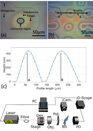
monochromatic light source we can calculate the height of the mem-brane separation from the device substrate using the wavelength of the light and the number of interference fringes counted from the contact point of the diamond and silica substrate. Height values,d, were cal-culated for each maxima and minima point of the interference fringes as
= d nλ
4, where n is an integer number. Additionally, points at the fringe
full-width-half-maxima were used to calculate height values equal to mλ
8, where m is an odd integer number. This data can be seen inFig. 4
which also shows an approximate height morphology using interpola-tion between the known points; the black vertical lines denote the po-sitions of the Si waveguides. The calculated height profile shows a central contacted region within the racetrack with the height of the membrane located directly above the waveguides varying with the asymmetry of the bond. The height of the membrane then reaches a maximum over a position that may not correspond to the position of the waveguides as is demonstrated inFig. 4. As the diamond across the bus waveguide only requires deformation across one axis in this case, the material bonds back to the substrate over distances of ~10μm. In the case of the racetrack resonator the diamond is required to deform over two axes limiting the local gradient with complex dependencies on membrane thickness and the locations of surrounding surface-contacted regions.
4. Optical probe measurements
The optical quality of the bond for use in integrated optical appli-cations was also investigated. To do this we used an end-fire rig with a lensed single modefibre and coupled it to the end facet of a bus wa-veguide for a resonator bonded beneath the diamond. A schematic of the optical setup is shown inFig. 5. All of the measurements reported were taken from an all-pass ring resonator with characteristics defined inSection 2earlier and transmission spectra taken at telecommunica-tion wavelengths. By curvefitting the transmission spectra shown in Fig. 7to the analytical model of an all-pass ring resonator [34], values for coupling coefficients, group index values, and distributed losses could be extracted. The power transmission intensity is described by the following equation:
= = − +
− +
T I I
a ra ϕ r ar ϕ ra
2 cos 1 2 cos ( )
pass
input
2 2
2
(1) whereais the single-pass amplitude transmission, and defined in terms of the power attenuation coefficient (α) of the system as follows: a2=exp(−αL). r is the amplitude self-coupling coefficient and its
[image:4.595.38.357.54.501.2]complimentary parameter is the amplitude cross-coupling coefficient defined as k. For a lossless system,r2+k2= 1 andk2=κthe power Fig. 4.(a) An optical image of a diamond membrane bonded over a Si resonator device showing interference fringes, a contacted region, and waveguides. (b) Optical image showing the line profile on which fringe analysis was conducted to calculate the height profile over the Si device, where A and B point to either end of the wave-guide resonator. (c) A height profile calculated from the fringe intensity over the line profile as shown in (b) with the black lines signifying the waveguide positions of the racetrack labelled again as A and B.
Fig. 6.Schematic of a racetrack resonator showing power cross coupling, transmission, and loss parameters.
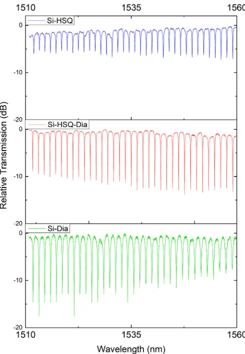
[image:5.595.332.533.283.440.2]Fig. 7.The normalised transmission spectra for (a) the as-fabricated Si device and when bonded with the diamond pre (b) and post (c) removal of the HSQ mask cap.
[image:5.595.40.285.315.669.2]Fig. 8.Extracted, and simulated group index values for the Si ring resonator alone, and when bonded with the 1μm diamond membrane with and without an HSQ cap. The measured results show a group index shift and gradient in agreement with the simulated values.
Fig. 9.A cross-sectional mode simulation showing the TE modal power dis-tribution at a wavelength of 1.535μm for a diamond membrane 70 nm above a Si waveguide with no HSQ cap.
[image:5.595.309.555.492.670.2]cross-coupling coefficient - a, r, and k are depicted inFig. 6.ϕis the single-pass phase shift, which is the product of the propagation constant and round trip length,βandLrespectively. The measurement data is fitted to the analytical solution using a least squares method, withκand
αas free parameters. The group index (ng=n−λ0dλdn
0, and the Q factor
=
(
Q f)
f Δ
0 can also be calculated from the measured resonant
wave-lengths and linewidths. The free spectral range is the wavelength spa-cing between adjacent resonances and is approximated by the equation,
λ n Lg
02, whereλ0is the wavelength of light,n
gis the group index, andLis
the length for 1 round trip of the cavity. The measurements were taken for three different cases detailed earlier to demonstrate an increasing mode interaction with the diamond and the transmission spectra are shown inFig. 7. From the spectra inFig. 7it can be seen that the free spectral range differs between the cases and therefore so does the re-sulting group index which is shown inFig. 8. It can be seen from the plot that the group index measurements match that of the FDE model calibrated to the as-fabricated Si waveguide case. In the case of the diamond bonded to the Si devices with the HSQ cap present, the group index measurements shift downwards and are also in agreement with simulations. The gradient of the group index is also seen to change from a positive to negative trend when bonded with the diamond as the si-mulations predicted. In the case for the diamond bonded to the device with the cap removed, the group index is reduced further but does not reach the simulated values. The measured results of the resonator do not match the simulated group index values for a hybrid diamond-si-licon device due to varying degrees of contact across the racetrack re-sonator. This is in agreement with analysis of the optical image dis-cussed earlier inSection 3. The deformation of the diamond membrane over the resonator device, which has a complex surrounding geometry as shown inFig. 4, has a contact point that is off-centre and interference fringes that are asymmetric. As a result the diamond-silicon contact is
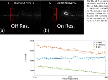
not fully consistent around the resonator. The result of this non-trivial surface geometry is equivalent to a diamond membrane with an average air gap in the order of 10s of nanometres and thus a less than simulated modal overlap, with a higher measured group index. A si-mulation of an average 70 nm air gap between the diamond and Si interface over the full resonator shows reasonable matching with the experimental results. To compare this case with the earlier confinement simulations inFig. 1a corresponding TE mode calculation at a wave-length of 1.535μm with the 70 nm gap present is shown inFig. 9where the confinement to the Si device is 70% and the diamond 6%. A second property of the resonator that allows assessment of the diamond-silicon interface is the power cross coupling coefficient and is shown inFig. 10. This is a dimensionless value used to characterise the interaction of the resonator with the bus waveguide. InFig. 1it can be seen that in the case of the diamond bonded with the HSQ cap still in place the con-finement has been shown not to change greatly, howeverFig. 10shows a reduction in power cross coupling coefficient. This can be explained by the effective index of the two interfaced materials, the device now clad with diamond rather than air. The presence of the diamond re-duces the overall effective index difference between the bus waveguide and resonator and thus reduces slightly the cross coupling coefficient compared with that of the as fabricated case. It can also be seen in Fig. 10that in the presence of the bonded diamond, with no HSQ cap, that the coupling coefficient has increased relative to the as fabricated Si device. Also as the injection wavelength is increased a larger cou-pling coefficient is observed. Both of these factors are explained by a larger mode overlap between the Si and the diamond membrane which increases with larger wavelengths and facilitates an increased power transfer between the bus guide and resonator. Thesefigures show that the membrane, after the HSQ has been removed, is in close enough proximity to the Si device to facilitate optical interaction between the two. Using an infrared (IR) camera positioned above the hybrid Si-Fig. 11.(a) A top scattering image of a 1μm diamond membrane bonded to a Si ring resonator offresonance. The red dashed line marks where the edge of the diamond is, and the red box highlights the scattering at this edge. (b) The resonator was tuned into resonance, and again with the red lines and box highlighting the edge of the diamond and scattering respectively. (For interpretation of the references to colour in this figure legend, the reader is referred to the web version of this article.)
[image:6.595.46.456.56.362.2]diamond device, scattered light was observed, with the diamond bonded, whilst the device was on and offresonance shown inFig. 11. It can be seen that the amount of vertical scattering is not discernibly different when measured from the Si waveguide alone or from the Si waveguide underneath the diamond suggesting the hybrid device had a low additional propagation loss. When the laser is tuned to a wave-length that is resonant with the racetrack cavity, the scattered light at the diamond edge is contrasted more clearly due to a large reduction in propagating light through the bus waveguide. This point source of scattered light at the diamond edge is also not noticeably different to that of the Si device's propagation losses showing that this interface does not add a large amount of optical loss. The added distributed losses of the ring itself which were extracted by the curvefitting method as detailed above, corroborated thesefindings and showed an added loss of 0.4 dB per round trip. Finally we measured loaded Q-factors for the three cases detailed before and found mean averaged values of 22.3k for the silicon device alone, 30.8k for the Si-HSQ-Dia, and 10.8k for the Si-Dia. The data has been plotted with trend lines inFig. 12. The wa-velength dependent loaded Q-factor is dominated by the inverse re-lationship with power cross coupling coefficients of each device case.
5. Conclusion
In conclusion we have shown that thin, free-standing SC diamond membranes can be integrated with photonic devices fabricated on more mature platforms. The mechanical and optical qualities of the bond were evaluated using SEM, optical interference calculations, and transmission spectra before and after the diamond was bonded. Group index dispersion measurements were conducted and compared with simulated values and found to be in good agreement, demonstrating an optical interaction with the diamond membrane. A low added loss of 0.4 dB per turn was achieved and a Q-factor of around 10k for the hybrid diamond-silicon resonator was found. By choosing relevant host-substrate materials, this integration technique could be used for a wide range of applications spanning several wavelength ranges.
Acknowledgements
We would like to thank C. Klitis and M. Sorel for providing the silicon devices. The research data associated with this paper are available at: https://doi.org/10.15129/7da6a6a3-b298-4e4a-b720-94a699017f61. Funding information
This work was supported by the EPSRC [EP/P013597/1], the National Quantum Information Technology Hub [EP/M013243/1], and Fraunhofer UK [EP/L015315/1].
References
[1] I. Aharonovich, A.D. Greentree, S. Prawer, Diamond photonics, Nat. Photonics 5 (2011) 397–405.
[2] P. Latawiec, V. Venkataraman, M.J. Burek, B.J.M. Hausmann, I. Bulu, M. Lončar, On-chip diamond Raman laser, Optica 2 (2015) 924.
[3] F. Gao, J. Van Erps, Z. Huang, H. Thienpont, R.G. Beausoleil, N. Vermeulen, Directional coupler based on single-crystal diamond waveguides, IEEE J. Sel. Top. Quantum Electron. 24 (2018) 1–9.
[4] B.J.M. Hausmann, I. Bulu, V. Venkataraman, P. Deotare, M. Lončar, Diamond nonlinear photonics, Nat. Photonics 8 (2014) 369–374.
[5] M.W. McCutcheon, M. Loncar, Design of a silicon nitride photonic crystal nano-cavity with a quality factor of one million for coupling to a diamond nanocrystal, Opt. Express 16 (2008) 19136.
[6] D. Englund, B. Shields, K. Rivoire, F. Hatami, J. Vučković, H. Park, M.D. Lukin, Deterministic coupling of a single nitrogen vacancy center to a photonic crystal cavity, Nano Lett. 10 (2010) 3922–3926.
[7] N. Thomas, R.J. Barbour, Y.C. Song, M.L. Lee, K.M.C. Fu, Waveguide-integrated single-crystalline GaP resonators on diamond, Opt. Express 22 (2014) 13555–13564.
[8] M. Gould, S. Chakravarthi, I.R. Christen, N. Thomas, S. Dadgostar, Y. Song, M.L. Lee, F. Hatami, K.-M.C. Fu, Large-scale GaP-on-diamond integrated photonics
platform for NV center-based quantum information, J. Opt. Soc. Am. B 33 (2016) B35.
[9] M. Gould, E.R. Schmidgall, S. Dadgostar, F. Hatami, K.M.C. Fu, Efficient extraction of zero-phonon-line photons from single nitrogen-vacancy centers in an integrated GaP-on-diamond platform, Phys. Rev. Appl. 6 (2016) 2–7.
[10] P.E. Barclay, K.M.C. Fu, C. Santori, A. Faraon, R.G. Beausoleil, Hybrid nanocavity resonant enhancement of color center emission in diamond, Phys. Rev. X 1 (2011) 1–7.
[11] P.E. Barclay, K.M.C. Fu, C. Santori, R.G. Beausoleil, Chip-based microcavities cou-pled to nitrogen-vacancy centers in single crystal diamond, Appl. Phys. Lett. 95 (2009) 93–96.
[12] M.B. Panish, Temperature dependence of the energy gap in GaAs and GaP, J. Appl. Phys. 40 (1969) 163.
[13] P. Latawiec, V. Venkataraman, A. Shams-Ansari, M. Markham, M. Lončar, Integrated diamond Raman laser pumped in the near-visible, Opt. Lett. 43 (2018) 318.
[14] B.J.M. Hausmann, B. Shields, Q. Quan, P. Maletinsky, M. McCutcheon, J.T. Choy, T.M. Babinec, A. Kubanek, A. Yacoby, M.D. Lukin, M. Loncar, Integrated diamond networks for quantum nanophotonics, Nano Lett. 12 (2012) 1578–1582. [15] B.J.M. Hausmann, I.B. Bulu, P.B. Deotare, M. McCutcheon, V. Venkataraman,
M.L. Markham, D.J. Twitchen, M. Lončar, Integrated high-quality factor optical resonators in diamond, Nano Lett. 13 (2013) 1898–1902.
[16] A.H. Piracha, P. Rath, K. Ganesan, S. Kühn, W.H.P. Pernice, S. Prawer, Scalable fabrication of integrated nanophotonic circuits on arrays of thin single crystal diamond membrane windows, Nano Lett. 16 (2016) 3341–3347.
[17] A.H. Piracha, K. Ganesan, D.W.M. Lau, A. Stacey, L.P. McGuinness, S. Tomljenovic-Hanic, S. Prawer, Scalable fabrication of high-quality, ultra-thin single crystal diamond membrane windows, Nanoscale 8 (2016) 6860–6865.
[18] T.M. Babinec, B.J. Hausmann, M. Khan, Y. Zhang, J.R. Maze, P.R. Hemmer, M. Lončar, A diamond nanowire single-photon source, Nat. Nanotechnol. 5 (2010) 195–199.
[19] E. Neu, P. Appel, M. Ganzhorn, J. Miguel-Sanchez, M. Lesik, V. Mille, V. Jacques, A. Tallaire, J. Achard, P. Maletinsky, Photonic nano-structures on (111)-oriented diamond, Appl. Phys. Lett. 104 (2014) 4.
[20] J.L. Zhang, S. Sun, M.J. Burek, C. Dory, Y.-K. Tzeng, K.A. Fischer, Y. Kelaita, K.G. Lagoudakis, M. Radulaski, Z.-X. Shen, N.A. Melosh, S. Chu, M. Lončar, J. Vučković, Strongly cavity-enhanced spontaneous emission from silicon-vacancy centers in diamond, Nano Lett. 18 (2018) 1360–1365.
[21] M.J. Burek, C. Meuwly, R.E. Evans, M.K. Bhaskar, A. Sipahigil, S. Meesala, B. Machielse, D.D. Sukachev, C.T. Nguyen, J.L. Pacheco, E. Bielejec, M.D. Lukin, M. Lončar, Fiber-coupled diamond quantum nanophotonic interface, Phys. Rev. Appl. 8 (2017) 024026.
[22] A. Sipahigil, R.E. Evans, D.D. Sukachev, M.J. Burek, J. Borregaard, M.K. Bhaskar, C.T. Nguyen, J.L. Pacheco, H.A. Atikian, C. Meuwly, R.M. Camacho, F. Jelezko, E. Bielejec, H. Park, M. Lončar, M.D. Lukin, An integrated diamond nanophotonics platform for quantum-optical networks, Science 354 (2016) 847–850.
[23] L. Li, T. Schröder, E.H. Chen, M. Walsh, I. Bayn, J. Goldstein, O. Gaathon, M.E. Trusheim, M. Lu, J. Mower, M. Cotlet, M.L. Markham, D.J. Twitchen, D. Englund, Coherent spin control of a nanocavity-enhanced qubit in diamond, Nat. Commun. 6 (2015) 6173.
[24] A. Faraon, C. Santori, Z. Huang, V.M. Acosta, R.G. Beausoleil, Coupling of nitrogen-vacancy centers to photonic crystal cavities in monocrystalline diamond, Phys. Rev. Lett. 109 (2012) 033604.
[25] M.J. Burek, N.P. De Leon, B.J. Shields, B.J. Hausmann, Y. Chu, Q. Quan, A.S. Zibrov, H. Park, M.D. Lukin, M. Lončar, Free-standing mechanical and photonic nanostructures in single-crystal diamond, Nano Lett. 12 (2012) 6084–6089. [26] I. Bayn, S. Mouradian, L. Li, J.A. Goldstein, T. Schröder, J. Zheng, E.H. Chen,
O. Gaathon, M. Lu, A. Stein, C.A. Ruggiero, J. Salzman, R. Kalish, D. Englund, Fabrication of triangular nanobeam waveguide networks in bulk diamond using single-crystal silicon hard masks, Appl. Phys. Lett. 105 (2014).
[27] H.A. Atikian, P. Latawiec, M.J. Burek, Y.-I. Sohn, S. Meesala, N. Gravel, A.B. Kouki, M. Lončar, Freestanding nanostructures via reactive ion beam angled etching, APL Photonics 2 (2017) 051301.
[28] S. Mouradian, N.H. Wan, T. Schröder, D. Englund, Rectangular photonic crystal nanobeam cavities in bulk diamond, Appl. Phys. Lett. 111 (2017).
[29] N.H. Wan, S. Mouradian, D. Englund, Two-dimensional photonic crystal slab na-nocavities on bulk single-crystal diamond, Appl. Phys. Lett. 112 (2018). [30] M.J. Burek, Y. Chu, M.S. Liddy, P. Patel, J. Rochman, S. Meesala, W. Hong, Q. Quan,
M.D. Lukin, M. Loncar, High quality-factor optical nanocavities in bulk single-crystal diamond, Nat. Commun. 5 (2014) 1–7.
[31] M.J. Strain, C. Lacava, L. Meriggi, I. Cristiani, M. Sorel, Tunable Q-factor silicon microring resonators for ultra-low power parametric processes, Opt. Lett. 40 (2015) 1274.
[32] C.L. Lee, E. Gu, M.D. Dawson, I. Friel, G.A. Scarsbrook, Etching and micro-optics fabrication in diamond using chlorine-based inductively-coupled plasma, Diam. Relat. Mater. 17 (2008) 1292–1296.
[33] Y. Tao, C. Degen, Facile fabrication of single-crystal-diamond nanostructures with ultrahigh aspect ratio, Adv. Mater. 25 (2013) 3962–3967.