On-chip implementation of the probabilistic
quantum optical state comparison amplifier
D
AVIDW. C
ANNING,
1R
OSSJ. D
ONALDSON,
1,*S
EBABRATAM
UKHERJEE,
1,3R
OBERTJ. C
OLLINS,
1L
UCAM
AZZARELLA,
2U
GOZ
ANFORLIN,
1J
OHNJ
EFFERS,
2R
OBERTR. T
HOMSON,
1 ANDG
ERALDS. B
ULLER11Scottish Universities Physics Alliance, Institute of Photonics and Quantum Sciences, School of Engineering
and Physical Sciences, Heriot-Watt University, David Brewster Building, Edinburgh EH14 4AS, UK
2Scottish Universities Physics Alliance, Department of Physics, University of Strathclyde, John Anderson
Building, 107 Rottenrow, Glasgow G4 0NG, UK
3Current address: Department of Physics, The Pennsylvania State University, University Park, PA 16802,
USA
Abstract: Propagation losses in transmission media limit the transmission distance of optical signals. In the case where the signal is made up of quantum optical states, conventional deterministic optical amplification schemes cannot be used to increase the transmission distance as the copying of an arbitrary and unknown quantum state is forbidden. One strategy that can offset propagation loss is the use of probabilistic, or non-deterministic, amplification schemes - an example of which is the state comparison amplifier. Here we report a state comparison amplifier implemented in a compact, fiber-coupled femtosecond laser-written waveguide chip as opposed to the large, bulk-optical components of previous designs. This pathfinder on-chip implementation of the quantum amplifier has resulted in several performance improvements: the polarization integrity of the written waveguides has resulted in improved visibility of the amplifier interferometers; the potential of substantially-reduced losses throughout the amplifier configuration; and a more compact and environmentally-stable amplifier which is scalable to more complex networks.
Published by The Optical Society under the terms of theCreative Commons Attribution 4.0 License. Further distribution of this work must maintain attribution to the author(s) and the published article’s title, journal citation, and DOI.
1. Introduction 1.1. Background
The no-cloning theorem forbids the copying of an unknown quantum state [1] and gives rise to a minimum bound on the amount of noise that an ideal deterministic amplifier must necessarily add to a signal [2]. It also places a fundamental limit on the amount of information that an eavesdropper can extract from a signal composed of non-orthogonal states which is the foundation on which the security of quantum communications protocols is built [3]. For any communications protocol, classical or quantum, to be implemented in real-world applications, information carriers must be distributed over lossy communication channels and measured using imperfect detectors. Propagation loss and detector inefficiency both serve to reduce the maximum transmission range and decrease the communication rate. In the classical channels of fiber optic telecommunications networks, these loss mechanisms can be mitigated using deterministic amplification of the signal at periodic intervals throughout the channels. This solution is ineffective in the quantum domain - where the information carriers are single-photons or, more often, weak coherent states - as even
#373277 https://doi.org/10.1364/OE.27.031713
Research Article Vol. 27, No. 22 / 28 October 2019 /Optics Express31714
the minimum added noise of the ideal amplifier makes the amplified state useless for quantum communications purposes [4].
Probabilistic amplification aims to avoid the minimum noise requirement on an ideal determin-istic linear amplifier by removing the requirement that the amplifier works every time [5]. The first probabilistic amplifier was devised by Ralph and Lund [6] based on Pegg et al.’s quantum scissors device [7]. It was implemented experimentally soon after their proposal [8,9] and probabilistic amplification has since developed into a burgeoning field of research. Ralph and Lund’s amplifier is an example of aphase-insensitiveprobabilistic amplifier. Further work on quantum scissors style schemes followed [10–14] and other phase-insensitive probabilistic amplifiers have been proposed and implemented based on photon addition and subtraction [15–17], noise addition followed by photon subtraction [16–19], and weak measurement [20,21]. Phase-insensitive probabilistic amplifiers are fundamentally limited to operating at very low success probability in order to achieve high fidelity, however,phase-sensitiveprobabilistic amplifiers are subject to less stringent bounds [5]. Phase-sensitive probabilistic amplification schemes have been proposed based on unambiguous state discrimination [22] and state comparison amplification [23–25]. Most probabilistic amplification schemes generally try to herald successful amplification events via success criteria (measured by the amplifier), although non-heralded schemes have also been proposed such as the use of a non-heralded probabilistic amplifier to improve a signal nulling binary receiver [26].
In addition to the fundamental challenges, there are also practical challenges that quantum communications technologies must address; a commercially viable implementation of a quantum-enhanced device would ideally be scalable, modular, and standardized. Inspired by integrated electronics, there has been intense interest in recent years towards re-scaling quantum information protocols from bulk optical systems to the miniaturized area of integrated optical devices [27–29]. Integrated photonic components are inherently more compact and have the potential to be produced en masse in commercial fabrication facilities for relatively low cost.
There are a variety of different platforms that are being investigated for fabrication of integrated optical devices and each have their own benefits and drawbacks. The advanced infrastructure that has already been developed for the electronics industry makes it attractive to use silicon or III-V compound semiconductor systems. These techniques produce highly compact devices but they suffer from high propagation losses [28], and, while the technology for coupling electrical signals on- and off-chip is advanced, the same cannot be said for coupling of light which remains a non-trivial task due to the large size of a single-mode fiber core in comparison to the resultant waveguides [30]. These drawbacks are improved (at some cost) by using glass waveguides such as etched silica-on-silicon or writing waveguides directly into glass using femtosecond laser writing (FLW).
1.2. Femtosecond laser writing
FLW [31–33] is a laser-based manufacturing technique enabling fabrication of three-dimensional micro-optic structures inside transparent dielectric materials. Due to nonlinear absorption processes, focused sub-picosecond laser pulses can permanently change the refractive index of the material allowing the direct inscription of optical waveguides. The unique capabilities of this fabrication technique can facilitate the future development of many fields including telecommunication, astrophotonics, and nonlinear dynamics, as well as help us to understand various intriguing phenomena in photonic networks [34–36].
birefringence and optical axis orientation [42]. In parallel with the technological developments described above, proof of principle quantum devices have been demonstrated using laser-written components, including quantum devices for state tomography [39], Hadamard [40] and CNOT [43] quantum logic gates, and integrated quantum memories in rare-earth-doped crystals [44].
FLW is a comparatively recent innovation and does not yet have the mature infrastructure of silicon and III-V manufacturing. However, it has the advantage that it can be used to create truly three-dimensional waveguide structures. Additionally, when using an appropriate beam-shaping method, FLW can produce waveguides with a circular cross-section [45], and therefore reduced birefringence, making the resulting waveguides highly suitable for applications that require the preservation of polarization and phase [28]. This fabrication technique provides excellent control over the shape of the fundamental mode, allowing for better mode matching and reduced on-chip coupling losses. Additionally, research has commenced into automation of the waveguide inscription process [46], offering the prospect of commercial manufacturing of multiple waveguide units in the future
No single platform currently provides the full range of capabilities required for all quantum information tasks and, for the moment, it is important to choose the platform that best suits the purposes of the device. We chose to implement the first on-chip implementation of the state comparison amplifier (SCAMP) using a FLW manufactured chip as the low birefringence of the waveguides ensured phase stability (crucial for state comparison of phase encoded states), the comparatively low coupling loss from fiber to the device maximized the effective intensity gain of the on-chip implementation, and the fast turnaround for creating prototypes aids investigation. This paper reports the first step towards fully on-chip state comparison amplification, which has been achieved by implementing the fundamental core beamsplitters of the amplifier in compact on-chip integrated directional couplers fabricated using FLW.
1.3. State comparison amplification
The SCAMP is a probabilistic amplifier operating on a known set of coherent state signals of arbitrary dimension. A case of interest for quantum communication is when the alphabet is composed of the states having the same mean photon number|α|2and whose phase belongs to
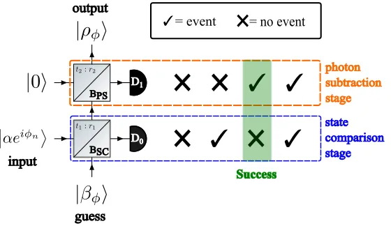
the setAN ={φn}, where 1≤n≤N,n∈Z+and 0≤φn=2Nπ(n−1)<2π[23]. The amplifier consists of two stages: astate comparisonstage, and aphoton subtractionstage. In what we will refer to in what follows as thestandardSCAMP setup [24], the state comparison stage consists of a single state-comparison operation and the photon subtraction stage consists of a single photon subtraction operation; this setup is summarized schematically in Fig.1.
Theinputsignal state which is to be amplified,|αeiφni, has phase chosen uniformly at random
fromAN, with αbeing real, and is incident at one input of a beamsplitter (with amplitude transmission and reflection coefficients given byt1andr1respectively and denoted BSCin the
figure). At the other input aguesscoherent state is incident,|βφi, the amplitude of which is that of the input modified by a factor oft1/r1:
|βφi=|t1eiφα/r1i with φ∈ AN (1) where the phaseφis chosen uniformly at random over the alphabet since there is noa priori
knowledge on the probability distribution for the input signal. This beamsplitter combined with a single-photon detector (operating in Geiger mode) monitoring one of the output arms, D0, forms
the state comparison stage. In the case that the phase of the guess has been chosen correctly the state incident on the state comparison detector, D0, is the vacuum state and the state output
into the other mode is the input state amplified by a factor of 1/r1, i.e. |αeiφn/r1i. On the other
Research Article Vol. 27, No. 22 / 28 October 2019 /Optics Express31716 photon subtraction stage state comparison stage output input guess BSC BPS
✓
❌
❌
✓
❌ ❌
✓ ✓
Success ❌= no event ✓= eventD1
D0
Fig. 1. Schematic representation of the standard SCAMP. When the phase of the input is guessed correctly the output of the SCAMP is the input state perfectly amplified by the nominal gain,g=r1t2. The output is post-selected based on D0registering no click and D1
registering a click to indicate the likelihood that the guess was correct.
was correct. This motivates the inclusion of the photon subtraction stage where the output of the state comparison stage is interfered with the vacuum at a second, highly transmitting, beamsplitter (with amplitude transmission and reflection coefficients given byt2andr2 respectively, with t2 r2, and denoted BPSin the figure) [23]. One output mode is again monitored by a second
single-photon detector D1. The intensity of light incident on D1is greatest for a correct guess
meaning that a correct guess is more likely to cause a detection event at D1than an incorrect
guess. Thus, a second success criterion can be defined as the condition that a detection event is registered at D1.
The other output of BPSis taken to be the output of the SCAMP, ρφ=(r12+t12ei(φ−φn))gαeiφn
E
(2)
where thenominal gainof the standard SCAMP has been defined asg=t2/r1. We note that the
output of the SCAMP is a perfect linear amplification of the input,gαeiφn, if (and only if) the
guess was correct (φ=φn) [2]. Without loss of generality we will setφn=0 for the rest of the
paper.
The running operation of the amplifier is then to condition the output signal based on having met both of the success criteria defined above. It is important to note that for all cases, except the special case where the state comparison beamsplitter is balanced (t1 =r1=1/√2) and the
phase alphabet is binary (N=2), there is still a non-zero probability of an incorrect guess that
has met the first success criterion also meeting the second criterion. Furthermore, in a practical implementation an incorrect guess could meet both criteria even in the balanced binary case as the second success criterion could be met by a detector dark count or photons incorrectly routed due to experimental imperfections. Therefore, the output of the SCAMP, conditioned on the success criteria having been met, is still a statistical mixture of the perfectly amplified target state,|gαi, and the other possible output states corresponding to incorrect guesses and can be
described by the following density operator [23]
ˆ
ρS = Õ
φ∈AN
[image:4.612.171.451.100.262.2]pφ|Sρφ ρφ (3)
Fig. 1. Schematic representation of the standard SCAMP. When the phase of the input is guessed correctly the output of the SCAMP is the input state perfectly amplified by the nominal gain,g=rt21. The output is post-selected based on D0registering no click and D1
registering a click to indicate the likelihood that the guess was correct.
In a practical system, non-unity detector efficiencies as well as the existence of the vacuum state in the coherent state superposition mean that the absence of a detection event does not allow us to infer with absolute certainty that light was not incident on the detector, i.e. that the guess was correct. This motivates the inclusion of the photon subtraction stage where the output of the state comparison stage is interfered with the vacuum at a second, highly transmitting, beamsplitter (with amplitude transmission and reflection coefficients given byt2andr2respectively, with
t2r2, and denoted BPSin the figure) [23]. One output mode is again monitored by a second
single-photon detector D1. The intensity of light incident on D1is greatest for a correct guess
meaning that a correct guess is more likely to cause a detection event at D1than an incorrect
guess. Thus, a second success criterion can be defined as the condition that a detection event is registered at D1.
The other output of BPSis taken to be the output of the SCAMP,
|ρφi =|(r12+t21ei(φ−φn))gαeiφni (2) where thenominal gainof the standard SCAMP has been defined asg=t2/r1; theintensity gain
on the signal is given by the square of this value,g2. We note that the output of the SCAMP is a
perfect linear amplification of the input,|gαeiφni, if (and only if) the guess was correct (φ=φn) [2]. Without loss of generality we will setφn=0 for the rest of the paper.
The running operation of the amplifier is then to condition the output signal based on having met both of the success criteria defined above. It is important to note that for all cases, except the special case where the state comparison beamsplitter is balanced (t1=r1=1/√2) and the
phase alphabet is binary (N=2), there is still a non-zero probability of an incorrect guess that
described by the following density operator [23]
ˆ
ρS= Õ φ∈AN
pφ|S|ρφihρφ| (3)
wherepφ|Sis the probability that the conditioned output contains the state corresponding to theφ guess. This probability can be related to the detection probability via Bayes’ rule via the formula:
pφ|S= Í pS|φpφ φ∈ANpS|φpφ
, (4)
by estimatingpS|φby:
pS|φ= 1− ˜ C0
φ Rφ
!C˜1
φ
Rφ (5)
where the ˜Ci
φare count rates corrected for the non-unity single-photon detection efficiency of the detectors and coupling losses, and the superscriptiindicates the detector. The probability,pφ, that the amplifier guess is out of phase with the input byφis again uniformly over the alphabet
since there is noa prioriknowledge on the probability distribution for the input signal. The standard SCAMP was first implemented experimentally with a nominal intensity gain g2=1.8 for evenly spaced phase alphabets of two-, four-, and eight-dimensions [24]. More recent
work demonstrates a higher gain implementation with nominal intensity gain 11.9, investigates a non-standard SCAMP setup where the photon subtraction stage consists of more than one photon subtraction (increasing fidelity at cost of success rate), and shows SCAMP performance to be robust against environmental noise [25]. It is important to note that the trueeffective intensity gainof any implementation is suppressed by the component losses.
2. Experimental method
The setup for this experiment comprised two nested fiber-based Mach-Zehnder interferometers (MZIs) and was almost identical to that of previous bulk-optical implementations of the standard SCAMP [24,25]. For brevity, the full experimental description, along with a schematic diagram, is presented in Appendix A. Where this experiment differed from previous implementations of the SCAMP was in the implementation of the state comparison beamsplitter, BSC, and the photon
subtraction beamsplitter, BPS. In previous implementations these were fiber-coupled standard
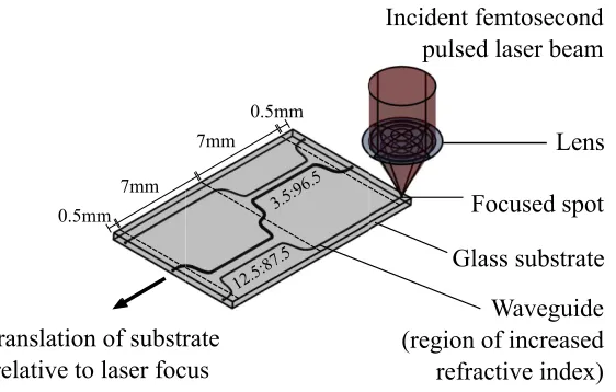
bulk optical components whereas here we made use of a FLW manufactured waveguide chip. For a systematic characterization, a complete three-waveguide-device (as illustrated schemat-ically in Fig.2) and an additional straight uncoupled waveguide were fabricated inside a 15-mm-long borosilicate glass (AF45) substrate. The glass substrate was mounted on air-bearing Aerotechx-y-ztranslation stages (ABL1000) and was translated at 6 mm/s through the focus (0.55 NA) of a 1-MHz train of circularly polarized sub-picosecond (∼350 fs) laser pulses to fabricate each waveguide. The laser inscription parameters, such as translation speed, pulse energy and numerical aperture of the focusing lens, were optimized to produce low-loss waveguides that were single-mode and well confined for light at wavelengths near 850 nm wavelength.
The total insertion (propagation+bend+input/output coupling) loss was measured after
aligning the device with commercially available V-groove arrays. The loss due to mode-mismatch was estimated to be less than 0.2 dB. The (average) on-chip loss for the waveguide(s) with one (two) directional coupler(s) was estimated to be 2.42 dB (4.58 dB). The on-chip propagation loss was estimated to be 0.017 dBmm−1and the average losses associated with the directional
couplers was estimated to be 2.28 dB per coupler.
Research Article Vol. 27, No. 22 / 28 October 2019 /Optics Express31718
Incident femtosecond
pulsed laser beam
Lens
Translation of substrate
relative to laser focus
Focused spot
Waveguide
(region of increased
refractive index)
Glass substrate
7mm 7mm 0.5mm 0.5mm 12.5: 87.5 3.5:96.5Fig. 2. Illustration of the FLW process for the waveguide chip used in this experiment. The two on-chip directional couplers are used as the implementation of the two beamsplitters, BSCand BPS, shown in Fig. 1. The symmetry of the waveguide structure allows for the chip
to be integrated in two orientations.
nominal intensity gain of 7.75 (25.09). The input-output coupling loss was estimated to be 1.70 dB on average.
The waveguide chip was integrated into the interferometric setup in both orientation 1 and orientation 2 where each orientation corresponds to an amplifier of different gain. Data was acquired for a binary (A2 ={0, π}) and a four-dimensional (A4 = {0, π/2, π,3π/2}) phase alphabet. We present the visibility for both the binary and four-dimensional phase alphabet alongside the amplifier figures of merit for the four-dimensional alphabet in the bulk of the paper. The figures of merit for the binary alphabet are presented in Appendix B.
3. Analysis and results
Following the detailed model of [25], the experimentally measured count ratesCφare related to the idealised count rates, ˜Cφ, of Eq. (5) via:
˜
Cφ=Rφ
"
1−
R
φ−Cφ Rφ
1 L#
(6)
whereRφis the laser pulse repetition rate multiplied by thea prioriprobability of an inputφ andLis the total intensity loss between the signal input and the detector (modelling imperfect detector efficiency as an additional source of loss). The corrected count rates can then be used to estimate the idealised intensity that is measured at each detector when the phase of the guess differs from the input byφ
Dφ2=ln Rφ Rφ−C˜φ
!
[image:6.612.175.456.110.289.2](7) Fig. 2.Illustration of the FLW process for the waveguide chip used in this experiment. The two on-chip directional couplers are used as the implementation of the two beamsplitters, BSCand BPS, shown in Fig.1. The symmetry of the waveguide structure allows for the chip to be integrated in two orientations.
chip is the same irrespective of which side of the chip is taken to be the input, we define two orientations of the chip. For clarity, this is the same as rotating the chip as shown in Fig.5, so that the side of the chip that was previously the input now becomes the output, and vice versa. We defineorientation 1in such a way that BSCis the (12.5):(87.5) coupler and BPSis the (3.5):(96.5)
coupler. On reversing the input direction of the chip we defineorientation 2such that BSCis
the (3.5):(96.5) coupler and BPSis the (12.5):(87.5) coupler. Consulting the nominal gain of the
standard SCAMP setup, orientation 1 (orientation 2) corresponds to a nominal intensity gain of 7.75 (25.09). The input-output coupling loss was estimated to be 1.70 dB on average.
The waveguide chip was integrated into the interferometric setup in both orientation 1 and orientation 2 where each orientation corresponds to an amplifier of different gain. Data was acquired for a binary (A2 = {0,π}) and a four-dimensional (A4 = {0,π/2,π, 3π/2}) phase
alphabet. We present the visibility for both the binary and four-dimensional phase alphabet alongside the amplifier figures of merit for the four-dimensional alphabet in the bulk of the paper. The figures of merit for the binary alphabet are presented in Appendix B.
3. Analysis and results
Following the detailed model of [25], the experimentally measured count ratesCφare related to the idealised count rates, ˜Cφ, of Eq. (5) via:
˜ Cφ =Rφ
"
1−Rφ−Cφ Rφ
1 L#
(6)
whereRφis the laser pulse repetition rate multiplied by thea prioriprobability of an inputφ
differs from the input byφ
|Dφ2|=ln Rφ Rφ−Cφ˜
!
(7)
With these definitions, various figures of merit can be estimated for the SCAMP and plotted against the input mean photon number per pulse,|α|2, which for each measurement was then
estimated from the count rates at the state comparison detector D0
|α|2= 1
2Nt2 1
Õ
φ∈AN
|D0φ|2 (8)
In order to quantify the experimental imperfection in the inner MZI we modify the description of the guess state amplitude, Eq. (1), to add a phase mismatch term,χ
|βφi =rt1
1exp{i(φ+χ)}α
(9)
We can estimate the cosine of the phase mismatch which corresponds to the visibility between a correctly guessed state and a guess state where the guess differs from the input byπ[25]
Visibility=cos(χ)= |D 0
π|2− |D00|2
|D0π|2+|D00|2 ( 10)
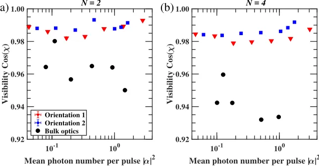
The visibilities for both orientations of the chip are presented in Figs.3(a) and3(b) alongside values for a previously published [25] equivalent bulk optical implementation of standard SCAMP. We observe an increase in the achievable visibility for all values of|α|2for both the binary and
four-dimensional phase alphabets. The increased visibility is especially pronounced in the four dimensional alphabet where we observe increased visibility on the order of 3.5%. This suggests improved polarization integrity in the waveguide chip when compared with the bulk optical components.
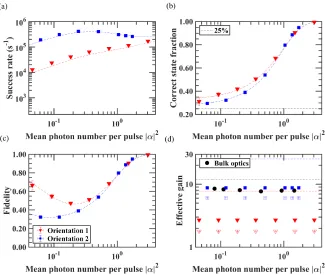
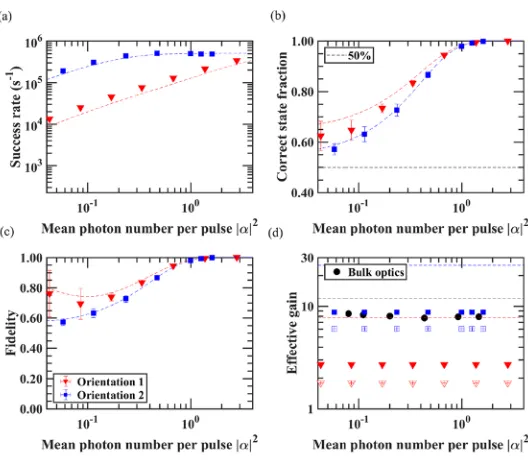
Further figures of merit for the SCAMP are presented in Figs.4(a)–4(d) for the four-dimensional phase alphabet (relevant, for example, for phase implementations of the BB84 protocol [47] or quantum digital signatures [48,49]). The equivalent results for the binary alphabet are presented in Figs.6(a)–6(d) in Appendix B. We first consider the overallsuccess rateof meeting the success criteria, that is given by:
Success Rate = Õ φ∈AN
RφpS|φ, (11)
wherepS|φhas been defined in Eq. (4). The success rate is presented in Fig.4(a), and increases with the mean photon number per pulse,|α|2, as expected.
Another two important figures of merit to asses the output quality are: thecorrect state fraction andfidelitywith respect to the target state. The correct state fraction is the probability that the output contains the correct amplified state given that the detectors indicate success, i.e.p0|Sin our notation.
The fidelity with respect to the target state is given byF=hgα|ρˆ|gαiand can be seen as the
Research Article Vol. 27, No. 22 / 28 October 2019 /Optics Express31720 With these definitions, various figures of merit can be estimated for the SCAMP and plotted against the input mean photon number per pulse,|α|2, which for each measurement was then
estimated from the count rates at the state comparison detector D0
|α|2= 1
2Nt12 Õ
φ∈AN
D0φ2 (8)
In order to quantify the experimental imperfection in the inner MZI we modify the description of the guess state amplitude, Eq. (1), to add a phase mismatch term,χ
βφ=
t1
r1exp{i(φ+χ)}α
(9)
We can estimate the cosine of the phase mismatch which corresponds to the visibility between a correctly guessed state and a guess state where the guess differs from the input byπ[25]
Visibility=cos(χ)=D 0
π2−D002
D0π2+D002
(10)
The visibilities for both orientations of the chip are presented in Fig. 3 alongside values for a previously published [25] equivalent bulk optical implementation of standard SCAMP. We observe an increase in the achievable visibility for all values of|α|2 for both the binary and
four-dimensional phase alphabets. The increased visibility is especially pronounced in the four dimensional alphabet where we observe increased visibility on the order of 3.5%. This suggests improved polarization integrity in the waveguide chip when compared with the bulk optical components.
10-1 100
Mean photon number per pulse | |2
0.92 0.94 0.96 0.98 1.00 Visibility Cos( )
N = 2
Orientation 1 Orientation 2 Bulk optics
10-1 100
Mean photon number per pulse | |2
0.92 0.94 0.96 0.98 1.00 Visibility Cos( )
N = 4
(b)
(a)
Fig. 3. Estimations of the cosine of the interferometric phase mismatch of the inner MZI. This quantity is interpreted as the visibility of the system and would equal one in a perfect system. The red triangles (blue squares) represent orientation 1 (orientation 2) of the waveguide chip. The black circles show the same quantity from a similar bulk optical experiment previously published in Ref. [25] for comparison. Each data point is the mean of 25 measurements and uncertainties were estimated by propagation of the standard error of the mean. Uncertainties are plotted for each data point but are in most cases smaller than the data point itself.
[image:8.612.143.465.98.266.2]Further figures of merit for the SCAMP are presented in Fig. 4 for the four-dimensional phase alphabet (relevant, for example, for phase implementations of the BB84 protocol [47] or
Fig. 3.Estimations of the cosine of the interferometric phase mismatch of the inner MZI. This quantity is interpreted as the visibility of the system and would equal one in a perfect system. The red triangles (blue squares) represent orientation 1 (orientation 2) of the waveguide chip. The black circles show the same quantity from a similar bulk optical experiment previously published in [25] for comparison. Each data point is the mean of 25 measurements and uncertainties were estimated by propagation of the standard error of the mean. Uncertainties are plotted for each data point but are in most cases smaller than the data point itself.
tomography detectors conditioned on success. The correct state fraction is thus given by:
p0|S =Í N0 φ∈ANNφ
, (12)
while the fidelity is given by:
F= Õ
φ∈AN Nφ
Í
φ∈ANNφ|h
gα|ρφi|2, (13)
We present thecorrect state fraction p0|Sin Fig.4(b) as a function of|α|2. As is predicted by theory we observe that for all values of|α|2the correct state fraction exceeds the best achievable
witha prioriprobability of 1/Nand increases towards unity with increasing input intensity. The fidelity is presented in Fig.4(c) and displays an initial decrease with mean photon number per pulse followed by a recovery towards unity as predicted by the theory.
Finally, it is important to quantify the true gain that is achieved by the amplifier. The nominal intensity gain,g2 =t2
2/r12, is suppressed by both the losses incurred by, and the imperfect visibility
of, the amplifier. For this reason we quantify theeffective intensity gainof the amplifier to be
g2
eff =g2LSCAMPt14+r41+2t21r12cos(χ) (14)
Fig. 4. Figures of merit for the SCAMP with four-dimensional (N=4) phase alphabet. (a)
success rate; the rate at which both of the success criteria are met. (b) correct state fraction; weighting of the target state in the output ensemble. (c) fidelity; the overlap of the output mixture with the target state. (d) effective gain; the nominal gain (g2=t22/r12, shown by the
dotted lines) suppressed by losses and imperfect visibility. The filled shapes represent the entirely on-chip gain omitting the loss incurred in taking the signal on- and off-chip. The empty shapes show the gain when accounting for on-/off-chip loss. Equivalent values for a previously published bulk optical implementation are shown for comparison [25]. In all four plots the red triangles (blue squares) represent orientation 1 (orientation 2) of the waveguide chip. In (a), (b), and (c) the dashed lines show the theoretical predictions for the associated values using the theory of Ref. [23] assuming unity detection efficiency. Data points and uncertainties are calculated as described in Fig. 3
4. Discussion
[image:9.612.144.469.187.462.2]In this paper we have presented the results of two partially on-chip implementations of the SCAMP where a coherent state signal was coupled from fiber optics onto on-chip FLW manufactured waveguides, underwent on-chip coherent state amplification, before being coupled back into fiber. We observed increased visibility due to improved polarization integrity in the on-chip implementation when compared with an otherwise equivalent implementation that used commercially available fiber-coupled bulk optical components. This improved visibility is observed at the cost of decreased effective gain due to increased losses introduced by this prototype version of the chip. The excess loss is, however, not prohibitive for the use of the amplifier on-chip as we have shown that, even accounting for coupling on and off chip, we can achieve similar gains to the bulk optical system, at a cost to fidelity, by varying transmission and reflection parameters. Strategies to recover the lost fidelity could include adding extra state comparisons (with feedforward state correction as demonstrated in [50]) or additional
Fig. 4. Figures of merit for the SCAMP with four-dimensional (N =4) phase alphabet.
(a) success rate; the rate at which both of the success criteria are met. (b) correct state fraction; weighting of the target state in the output ensemble. (c) fidelity; the overlap of the output mixture with the target state. (d) effective intensity gain; the nominal intensity gain (g2=t2
2/r21, shown by the dotted lines) suppressed by losses and imperfect visibility.
Research Article Vol. 27, No. 22 / 28 October 2019 /Optics Express31722
on-chip, and 1.72 (6.07) when on-/off-chip coupling is accounted for. For comparison, the equivalent bulk optical implementation (g2 =11.9) has mean effective intensity gain of 8.20. The
added suppression of the on-chip implementation is due to the increased on-/off-chip coupling when compared with a fiber splice, and the increased loss of the FLW manufactured directional couplers in comparison to the bulk optical components.
4. Discussion
In this paper we have presented the results of two partially on-chip implementations of the SCAMP where a coherent state signal was coupled from fiber optics onto on-chip FLW manufactured waveguides, underwent on-chip coherent state amplification, before being coupled back into fiber. We observed increased visibility due to improved polarization integrity in the on-chip implementation when compared with an otherwise equivalent implementation that used commercially available fiber-coupled bulk optical components. This improved visibility is observed at the cost of decreased effective intensity gain due to increased losses introduced by this prototype version of the chip. The excess loss is, however, not prohibitive for the use of the amplifier on-chip as we have shown that, even accounting for coupling on and off chip, we can achieve similar gains to the bulk optical system, at a cost to fidelity, by varying transmission and reflection parameters. To be clear, we do not mean to say that fidelity is affected intrinsically by switching from bulk optics to the FLW chip. However, equivalent effective intensity gain can be achieved for the chip by compensating for any extra loss (when compared with bulk optics) by implementing a higher nominal intensity gain which, in turn, causes a decrease in fidelity as predicted by [23]. To quantify this for our particular chip, orientation 2 achieves an effective intensity gain of 6.07 from a nominal intensity gain of 25.09, whereas the similar effective intensity gain of 8.20 in [25] was achieved with a nominal intensity gain of 11.9. Strategies to recover the lost fidelity could include adding extra state comparisons (with feedforward state correction as demonstrated in [50]) or additional photon subtractions at a cost to the success rate. Our results clearly illustrate that any future technological improvements in coupling light on and off of integrated photonic platforms, as well as in minimizing bending loss introduced by the directional couplers would directly translate to an enhanced effective intensity gain in the SCAMP.
The amplifier could be further miniaturised by implementing any of the following on-chip alongside the waveguides: phase modulation of the guess signal [51], the stability tuning of the optical path length, dynamic tuning of the transmittance and reflectance of the directional couplers (coarse tuning could provide re-configurable gain), or on-chip integration of the single-photon detectors [52].
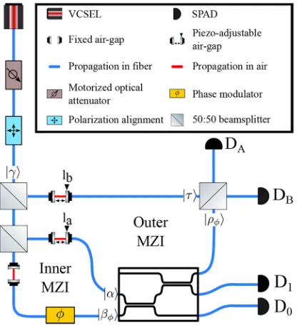
Fig. 5.A schematic representation of the experimental setup used in the partially on-chip SCAMP experiment. Note the symmetry of the chip on rotation by 180 degrees. By reversing the input and output ports of the chip it is possible to implement a SCAMP with a different nominal gain.
Appendix A. Experimental setup
The experimental setup is shown schematically in Fig.5. The initial source of coherent light, |γi, was a fiber-coupled vertical cavity surface-emitting laser (VCSEL) diode with a central
wavelength of 848.2 nm, spectral linewidth (full width at half maximum) of 0.11 nm, and pulsed at a repetition rate of 1 MHz with pulse duration of 300 ps. This light was attenuated to a low mean photon number per pulse by a motorized optical attenuator before, using stress induced birefringence (via polarization controllers), the light emitted by the laser was aligned with the transmission axis of a 1000:1 extinction ratio fiber-coupled linear optical polarizer.
The light was then coupled into one input pigtail of a commercially available fiber-coupled bulk optical beamsplitter. This beamsplitter and all subsequent bulk optical components were fiber-coupled to fiber that was single-mode and polarization maintaining at the operational wavelength. The beamsplitter split the light into two identical lower amplitude weak coherent states at a balanced beamsplitter on entering the outer MZI. The state on the upper arm was retained as a reference state for the purpose of comparing the output state of the SCAMP with the idealized output state, or target state.
The state on the lower arm was again split by a second balanced beamsplitter on entering the inner MZI where the upper arm provided the input signal,|αi, which maintained a constant
phase, and the lower arm was modulated by a phaseφto form the guess signal. The phase
modulation was performed with a lithium niobate phase modulator which varied the phase in a cyclical fashion from the discrete set of phasesAN. Each of the four detectors, D0, D1, DA, and
DB, was a commercial thick-junction silicon single-photon avalanche diode (SPAD) operating in
Research Article Vol. 27, No. 22 / 28 October 2019 /Optics Express31724
During initial setup a timing calibration procedure was performed on each interferometer to ensure high performance prior to loss balancing being performed between the arms of both interferometers. Next, in order to loss balance the inner MZI, each arm of the inner MZI was blocked in turn and the intensity at D0was matched using the screw attenuator labelledla. This
corresponds to ensuring that the guess amplitude,βφ, is related to the signal amplitude,αby the expression given in Eq. (9). Then, in order to loss balance the outer MZI, each arm of the outer MZI was blocked in turn, while ensuring the intensity at D0was minimized (corresponding to a
correct guess,φ=0) and the intensity at DAand DBwas matched using the screw attenuator
labelledlb. This calibration procedure allows us to infer the relation of|τi, to the target amplified
state|gαi.
The experiment was operated at various values of|α|2by varying the intensity of|γiusing the
motorized attenuator. Custom software dynamically tuned the optical length differences (via piezo-adjustable air-gaps) to maximize the observed visibility calculated between theφ=0 and
φ=πpulses at D0and the cross-visibility between theφ=0 pulses at DAand DB. Minimum
thresholds for these values were set at 97% and 90% respectively and a measurement would be discarded if they were not reached. Each data point plotted in this paper is an average of twenty-five individual single second integration measurements that achieved, or exceeded, these thresholds.
[image:12.612.174.438.345.575.2]Appendix B. Figures of merit for the binary phase alphabet
Fig. 6.Figures of merit for the SCAMP with binary (N=2) phase alphabet. Conventions
are the same as in Figs.4(a)–4(d). Data points and uncertainties are calculated as described in Fig.3
Funding
Data availability
The data associated with this work can be downloaded from the Heriot-Watt data archive at https://doi.org/10.17861/ce38b87b-001a-480f-b03c-f0be6e5dc3bd
Acknowledgments
S.M. and R.R.T. thank Debaditya Choudhury for assistance in experimental aspects.
Disclosures
The authors declare no conflicts of interest.
References
1. W. Wootters and W. Zurek, “A Single Quantum Cannot Be Cloned,”Nature299(5886), 802–803 (1982). 2. C. M. Caves, “Quantum limits on noise in linear amplifiers,”Phys. Rev. D26(8), 1817–1839 (1982).
3. V. Scarani, H. Bechmann-Pasquinucci, N. J. Cerf, M. Dušek, N. Lütkenhaus, and M. Peev, “The security of practical quantum key distribution,”Rev. Mod. Phys.81(3), 1301–1350 (2009).
4. N. Gisin, G. Ribordy, W. Tittel, and H. Zbinden, “Quantum cryptography,”Rev. Mod. Phys.74(1), 145–195 (2002). 5. S. Pandey, Z. Jiang, J. Combes, and C. M. Caves, “Quantum limits on probabilistic amplifiers,”Phys. Rev. A88(3),
033852 (2013).
6. T. C. Ralph and A. P. Lund, “Nondeterministic Noiseless Linear Amplification of Quantum Systems,” inAIP Conf. Proc., vol. 1110 (2009), pp. 155–160.
7. D. T. Pegg, L. S. Phillips, and S. M. Barnett, “Optical State Truncation by Projection Synthesis,”Phys. Rev. Lett.
81(8), 1604–1606 (1998).
8. G. Y. Xiang, T. C. Ralph, A. P. Lund, N. Walk, and G. J. Pryde, “Heralded noiseless linear amplification and distillation of entanglement,”Nat. Photonics4(5), 316–319 (2010).
9. F. Ferreyrol, M. Barbieri, R. Blandino, S. Fossier, R. Tualle-Brouri, and P. Grangier, “Implementation of a Nondeterministic Optical Noiseless Amplifier,”Phys. Rev. Lett.104(12), 123603 (2010).
10. J. Jeffers, “Nondeterministic amplifier for two-photon superpositions,”Phys. Rev. A82(6), 063828 (2010). 11. N. Gisin, S. Pironio, and N. Sangouard, “Proposal for Implementing Device-Independent Quantum Key Distribution
Based on a Heralded Qubit Amplifier,”Phys. Rev. Lett.105(7), 070501 (2010).
12. C. I. Osorio, N. Bruno, N. Sangouard, H. Zbinden, N. Gisin, and R. T. Thew, “Heralded photon amplification for quantum communication,”Phys. Rev. A86(2), 023815 (2012).
13. S. Kocsis, G. Y. Xiang, T. C. Ralph, and G. J. Pryde, “Heralded noiseless amplification of a photon polarization qubit,”Nat. Phys.9(1), 23–28 (2013).
14. N. Bruno, V. Pini, A. Martin, and R. T. Thew, “A complete characterization of the heralded noiseless amplification of photons,”New J. Phys.15(9), 093002 (2013).
15. J. Fiurášek, “Engineering quantum operations on traveling light beams by multiple photon addition and subtraction,”
Phys. Rev. A80(5), 053822 (2009).
16. P. Marek and R. Filip, “Coherent-state phase concentration by quantum probabilistic amplification,”Phys. Rev. A
81(2), 022302 (2010).
17. A. Zavatta, J. Fiurášek, and M. Bellini, “A high-fidelity noiseless amplifier for quantum light states,”Nat. Photonics
5(1), 52–56 (2011).
18. M. A. Usuga, C. R. Müller, C. Wittmann, P. Marek, R. Filip, C. Marquardt, G. Leuchs, and U. L. Andersen, “Noise-powered probabilistic concentration of phase information,”Nat. Phys.6(10), 767–771 (2010).
19. J. Jeffers, “Optical amplifier-powered quantum optical amplification,”Phys. Rev. A83(5), 053818 (2011). 20. D. Menzies and S. Croke, “Noiseless linear amplification via weak measurements,” arXiv:0903.4181 [quant-ph]
(2009).
21. J. Ho, A. Boston, M. Palsson, and G. Pryde, “Experimental noiseless linear amplification using weak measurements,”
New J. Phys.18(9), 093026 (2016).
22. V. Dunjko and E. Andersson, “Truly noiseless probabilistic amplification,”Phys. Rev. A86(4), 042322 (2012). 23. E. Eleftheriadou, S. M. Barnett, and J. Jeffers, “Quantum Optical State Comparison Amplifier,”Phys. Rev. Lett.
111(21), 213601 (2013).
24. R. J. Donaldson, R. J. Collins, E. Eleftheriadou, S. M. Barnett, J. Jeffers, and G. S. Buller, “Experimental Implementation of a Quantum Optical State Comparison Amplifier,”Phys. Rev. Lett.114(12), 120505 (2015). 25. R. J. Donaldson, L. Mazzarella, R. J. Collins, J. Jeffers, and G. S. Buller, “A high-gain and high-fidelity coherent
state comparison amplifier,”Commun. Phys.1(1), 54 (2018).
26. M. Rosati, A. Mari, and V. Giovannetti, “Coherent-state discrimination via nonheralded probabilistic amplification,”
Phys. Rev. A93(6), 062315 (2016).
Research Article Vol. 27, No. 22 / 28 October 2019 /Optics Express31726
28. A. Orieux and E. Diamanti, “Recent advances on integrated quantum communications,”J. Opt.18(8), 083002 (2016). 29. F. Flamini, N. Spagnolo, and F. Sciarrino, “Photonic quantum information processing: a review,”Rep. Prog. Phys.
82(1), 016001 (2019).
30. L. Vivien and L. Pavesi,Handbook of Silicon Photonics(Taylor & Francis, 2016).
31. K. M. Davis, K. Miura, N. Sugimoto, and K. Hirao, “Writing waveguides in glass with a femtosecond laser,”Opt. Lett.21(21), 1729–1731 (1996).
32. R. R. Gattass and E. Mazur, “Femtosecond laser micromachining in transparent materials,”Nat. Photonics2(4), 219–225 (2008).
33. D. Choudhury, J. R. Macdonald, and A. K. Kar, “Ultrafast laser inscription: perspectives on future integrated applications,”Laser Photonics Rev.8(6), 827–846 (2014).
34. J. Bryant, R. R. Thomson, and M. J. Withford, “Focus issue introduction: recent advances in astrophotonics,”Opt. Express25(17), 19966–19967 (2017).
35. M. Tillmann, B. Dakić, R. Heilmann, S. Nolte, A. Szameit, and P. Walther, “Experimental boson sampling,”Nat. Photonics7(7), 540–544 (2013).
36. S. Mukherjee, D. Mogilevtsev, G. Y. Slepyan, T. H. Doherty, R. R. Thomson, and N. Korolkova, “Dissipatively coupled waveguide networks for coherent diffusive photonics,”Nat. Commun.8(1), 1909 (2017).
37. L. A. Fernandes, J. R. Grenier, P. R. Herman, J. S. Aitchison, and P. V. S. Marques, “Femtosecond laser fabrication of birefringent directional couplers as polarization beam splitters in fused silica,”Opt. Express19(13), 11992–11999 (2011).
38. A. M. Streltsov and N. F. Borrelli, “Fabrication and analysis of a directional coupler written in glass by nanojoule femtosecond laser pulses,”Opt. Lett.26(1), 42–43 (2001).
39. G. Corrielli, A. Crespi, R. Geremia, R. Ramponi, L. Sansoni, A. Santinelli, P. Mataloni, F. Sciarrino, and R. Osellame, “Rotated waveplates in integrated waveguide optics,”Nat. Commun.5(1), 4249 (2014).
40. R. Heilmann, M. Gräfe, S. Nolte, and A. Szameit, “Arbitrary photonic wave plate operations on chip: Realizing Hadamard, Pauli-X, and rotation gates for polarisation qubits,”Sci. Rep.4(1), 4118 (2015).
41. A. Crespi, R. Osellame, R. Ramponi, V. Giovannetti, R. Fazio, L. Sansoni, F. De Nicola, F. Sciarrino, and P. Mataloni, “Anderson localization of entangled photons in an integrated quantum walk,”Nat. Photonics7(4), 322–328 (2013). 42. L. A. Fernandes, J. R. Grenier, P. R. Herman, J. S. Aitchison, and P. V. S. Marques, “Stress induced birefringence
tuning in femtosecond laser fabricated waveguides in fused silica,”Opt. Express20(22), 24103–24114 (2012). 43. A. Crespi, R. Ramponi, R. Osellame, L. Sansoni, I. Bongioanni, F. Sciarrino, G. Vallone, and P. Mataloni, “Integrated
photonic quantum gates for polarization qubits,”Nat. Commun.2(1), 566 (2011).
44. G. Corrielli, A. Seri, M. Mazzera, R. Osellame, and H. de Riedmatten, “Integrated Optical Memory Based on Laser-Written Waveguides,”Phys. Rev. Appl.5(5), 054013 (2016).
45. M. Ams, G. Marshall, D. Spence, and M. Withford, “Slit beam shaping method for femtosecond laser direct-write fabrication of symmetric waveguides in bulk glasses,”Opt. Express13(15), 5676–5681 (2005).
46. Y. Wang, L. Hermann Negri, I. Chiamenti, I. Abe, and H. J. Kalinowski, “Automated System for Femtosecond Laser Writing of Photonic Structures,”J. Control. Autom. Electr. Syst.29(2), 153–162 (2018).
47. R. J. Hughes, G. L. Morgan, and C. G. Peterson, “Quantum key distribution over a 48 km optical fibre network,”J. Mod. Opt.47(2-3), 533–547 (2000).
48. R. J. Collins, R. Amiri, M. Fujiwara, T. Honjo, K. Shimizu, K. Tamaki, M. Takeoka, E. Andersson, G. S. Buller, and M. Sasaki, “Experimental transmission of quantum digital signatures over 90 km of installed optical fiber using a differential phase shift quantum key distribution system,”Opt. Lett.41(21), 4883–4886 (2016).
49. R. J. Collins, R. Amiri, M. Fujiwara, T. Honjo, K. Shimizu, K. Tamaki, M. Takeoka, M. Sasaki, E. Andersson, and G. S. Buller, “Experimental demonstration of quantum digital signatures over 43 dB channel loss using differential phase shift quantum key distribution,”Sci. Rep.7(1), 3235 (2017).
50. R. J. Donaldson, L. Mazzarella, U. Zanforlin, R. J. Collins, J. Jeffers, and G. S. Buller, “Quantum state correction using a measurement-based feedforward mechanism,”Phys. Rev. A100(2), 023840 (2019).
51. J. Thomas, M. Heinrich, P. Zeil, V. Hilbert, K. Rademaker, R. Riedel, S. Ringleb, C. Dubs, J.-P. Ruske, S. Nolte, and A. Tünnermann, “Laser direct writing: Enabling monolithic and hybrid integrated solutions on the lithium niobate platform,”Phys. Status Solidi A208(2), 276–283 (2011).
52. F. Najafi, J. Mower, N. C. Harris, F. Bellei, A. Dane, C. Lee, X. Hu, P. Kharel, F. Marsili, S. Assefa, K. K. Berggren, and D. Englund, “On-chip detection of non-classical light by scalable integration of single-photon detectors,”Nat. Commun.6(1), 5873 (2015).
53. U. Zanforlin, R. J. Donaldson, R. J. Collins, and G. S. Buller, “Analysis of the effects of imperfections in an optical heterodyne quantum random-number generator,”Phys. Rev. A99(5), 052305 (2019).
54. D. Malik, G. Kaushik, and A. Wason, “Performance evaluation of hybrid optical amplifiers in WDM system,”J. Opt.