Theses Thesis/Dissertation Collections
8-2015
Reliable Low-Latency and Low-Complexity Viterbi
Architectures Benchmarked on ASIC and FPGA
Vineeta Pannalal Singh
Follow this and additional works at:http://scholarworks.rit.edu/theses
This Master's Project is brought to you for free and open access by the Thesis/Dissertation Collections at RIT Scholar Works. It has been accepted for inclusion in Theses by an authorized administrator of RIT Scholar Works. For more information, please [email protected].
Recommended Citation
RELIABLE LOW-LATENCY ANDLOW-COMPLEXITYVITERBIARCHITECTURES
BENCHMARKED ON ASICANDFPGA
by
Vineeta Pannalal Singh
A Gradute Paper Submitted
in
Partial Fulfillment
of the
Requirements for the Degree of
MASTER OFSCIENCE
in
Electrical Engineering
Approved by:
PROF.
(GRADUATEPAPERADVISOR- DR. MEHRANMOZAFFARI-KERMANI)
PROF.
(DEPARTMENTHEAD- DR. SOHAILA. DIANAT)
DEPARTMENT OFELECTRICAL ANDMICROELECTRONICENGINEERING
COLLEGE OFENGINEERING
ROCHESTER INSTITUTE OF TECHNOLOGY
ROCHESTER, NEW YORK
Declaration
I hereby declare that except where specific reference is made to the work of others, the contents
of this dissertation are original and have not been submitted in whole or in part for
consider-ation for any other degree or qualificconsider-ation in this, or any other University. This dissertconsider-ation
is the result of my own work and includes nothing which is the outcome of work done in
collaboration, except where specifically indicated in the text.
Vineeta Pannalal Singh
I would like to thank my advisor Dr. Mehran Mozaffari-Kermani for his guidance and
feed-back which helped in the successful completion of my graduate research. Special thanks to
Professor Mark Indovina for his valuable help. I also thank Dr. Reza Azarderakhsh for his
Abstract
The Viterbi algorithm is commonly applied in a number of sensitive usage models including
decoding convolutional codes used in communications such as satellite communication,
cellu-lar relay, and wireless local area networks. Moreover, the algorithm has been applied to
auto-matic speech recognition and storage devices. In this thesis, efficient error detection schemes
for architectures based on low-latency, low-complexity Viterbi decoders are presented. The
merit of the proposed schemes is that reliability requirements, overhead tolerance, and
per-formance degradation limits are embedded in the structures and can be adapted accordingly.
We also present three variants of recomputing with encoded operands and its modifications
to detect both transient and permanent faults, coupled with signature-based schemes. The
in-strumented decoder architecture has been subjected to extensive error detection assessments
through simulations, and application-specific integrated circuit (ASIC) [32nm library] and
field-programmable gate array (FPGA) [Xilinx Virtex-6 family] implementations for
bench-mark. The proposed fine-grained approaches can be utilized based on reliability objectives
Contents v
List of Figures vii
List of Tables viii
1 Introduction 1
1.1 Viterbi Algorithm . . . 1
1.2 Fault Diagnosis . . . 3
1.2.1 Faults and Degrdation . . . 4
1.2.2 Fault Detection Techniques . . . 6
1.3 Objectives . . . 8
1.4 Thesis Outline . . . 9
2 Preliminaries 10 2.1 Binary Grouping (BBG) Approach . . . 10
2.2 Look-ahead-based Low-Latency Architectures . . . 11
2.3 Alternative to Look-ahead Approach . . . 12
3 Proposed Reliable Architectures 14 3.1 Unified Signature-based Scheme for CSA and PCSA Units within BMP . . . 14
Contents vi
4 Benchmarks and Assessments 28
4.1 Simulations for Fault Injection Models . . . 28
4.2 ASIC and FPGA Implementations . . . 29
5 Conclusions 33
5.1 Future Work . . . 33
1.1 Viterbi decoder block diagram. . . 2
2.1 Overall layered structure including theP1 processor architecture. . . 13
3.1 Sequential branch metric computation unit including CSA (PCSA) structures. 15 3.2 The CSA signature-based error detection approach (the shaded adders are vari-ants of the original ones with the proposed error detection schemes). . . 16
3.3 Signature-based PCSA error detection (the shaded adders include the pro-posed error detection schemes). . . 17
3.4 Self checking adder in the proposed scheme. . . 19
3.5 A variant of self checking adder utilized in the devised approach. . . 21
3.6 Recomputing with encoded operands for CSA. . . 23
3.7 PCSA error detection through recomputing with encoded operands. . . 25
List of Tables
4.1 Area, delay, and power consumption benchmark on ASIC for CSA
architec-ture. . . 29
4.2 PCSA area, delay, and power consumption benchmark on ASIC. . . 30
4.3 CSA benchmark through Xilinx Virtex-6 (xc6vlx75t-3ff484 device) FPGA
family. . . 30
4.4 Xilinx Virtex-6 FPGA implementations for PCSA. . . 31
4.5 Throughput, efficiency, and energy consumption benchmark on ASIC for CSA
and PCSA. . . 31
4.6 Xilinx Virtex-6 FPGA implementations for throughput and efficiency
Introduction
1.1
Viterbi Algorithm
The Viterbi algorithm was introduced in 1967 as an efficient method for decoding
convo-lutional codes [1], widely used in communication systems [2].This algorithm is utilized for
decoding the codes used in various applications including satellite communication, cellular,
and radio relay. It has proven to be an effective solution for a lot of problems related to
digital estimation. Moreover, the Viterbi decoder has practical use in implementations of
high-speed (5 to 10 Gb/s) serializer-deserializers (SERDESs) which have critical latency
con-straints. SERDESs can be further used in local area and synchronous optical networks of 10
Gb/s. Furthermore, they are used in magnetic or optical storage systems such as hard disk
drive or digital video disk [3].
The Viterbi algorithm process is similar to finding the most-likely sequence of states,
re-sulting in sequence of observed events and, thus, boasts of high efficiency as it consists of
finite number of possible states [4–7]. It is an effective implementation of a discrete-time
fi-nite state Markov process perceived in memoryless noise and optimality can be achieved by
following the maximum-likelihood criteria [8]. It helps in tracking the stochastic process state
1.1 Viterbi Algorithm 2
Branch metric unit
(BMU)
Branch metric
precomputation (BMP)
Add-compare-select
(ACS)
R
Survivor path memory
unit (SMU)
Output
signal
Input
[image:12.595.78.519.122.310.2]signal
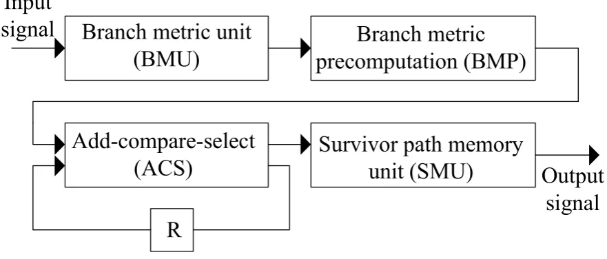
Figure 1.1: Viterbi decoder block diagram.
top-level architecture for Viterbi decoders is shown in Fig.1.1. As seen in this figure, Viterbi
decoders are composed of three major components: branch metric unit (BMU),
add-compare-select (ACS) unit, and survivor path memory unit (SMU). BMU generates the metrics
corre-sponding to the binary trellis depending on the received signal, which is given as input to ACS
which, then, updates the path metrics. The survival path is updated for all the states and is
stored in the additional memory. SMU is responsible for managing the survival paths and
giv-ing out the decoded data as output. BMU and SMU units happen to be purely forward logic.
ACS recursion consists of feedback loops; hence, its speed is limited by the iteration bound
[11]. Hence, the ACS unit becomes the speed bottleneck for the system. M-step look-ahead
technique can be used to break the iteration bound of the Viterbi decoder of constraint length
K[12–18]. A look-ahead technique can combine several trellis steps into one trellis step, and ifM>K, then throughput can be increased by pipelining the ACS architecture, which helps in solving the problem of iteration bound, and is frequently used in high-speed communication
systems. Branch metric precomputation (BMP) which is in the front end of ACS is resulted
due to the look-ahead technique and it dominates the overall complexity and latency for deep
steps and combines binary trellis of multiple-steps into a single complex trellis of one-step.
BMP dominates the overall latency and complexity for deep look-ahead architectures. Before
the saturation of the trellis, only add operation is needed. After the saturation of the trellis, add
operation is followed by compare operation where the parallel paths consisting of less metrics
are discarded as they are considered unnecessary.
Although Viterbi algorithm architectures are used commonly in decoding convolutional
codes, in the presence of very-large-scale integration (VLSI) defects, erroneous outputs can
occur which degrade the accuracy in decoding of convolutional codes.
1.2
Fault Diagnosis
A fault in a system can be defined as a deviation from the expected working of the system
which can be due to a defect of some components of the circuit. They can be temporary or
permanent. Permanent faults are called as Solid or Hard faults and can result due to the
wear-ing out or breakwear-ing of components. Temporary faults can be referred to as soft faults and these
faults can be classified as intermiitent or transient as it occurs only at certain intervals of time.
An intermittent fault occurs when the component is developing a permanent fault. A transient
fault can result due to some external disturbance like power supply fluctuations. Depending
upon the effect of faults, they can be classified as parametric or logical. A parametric fault
causes a change in speed, voltage or current as it alters the circuit parameter magnitude, while
a logical fault ends up changing the Boolean function originally realized by the circuit. Delay
fault which results due to slow gates is an important parametric fault and it leads to problems
of critical races or Hazards. Fault extent can be local or distributed. A distributed fault
af-fects multiple variables, whereas a local fault afaf-fects single variable. The clock malfunction
is an example of a distributed fault while a logical fault is an example of a local fault. With
the VLSI technology developing, the number of components on a single chip are increasing
1.2 Fault Diagnosis 4
research area.
1.2.1
Faults and Degrdation
Depending on the behavior of the system, logical faults represent the behavior of the system
modeled. Logical faults has three important classes:
A) Stuck-at-faults: A single stuck-at-fault happens when either one of the inputs or the
output of the logic gate is fixed at either a logic 1 (stuck-at-1) or a logic 0 (stuck-at-0). They
can be denoted by abbreviations as s-a-1 and s-a-0 respectively. This fault model is a good
representation for types of defects such as open circuits and short circuits. The stuck-at model
can also represent multiple faults which results when multiple signal lines are stuck at logic 0
or logic 1.
B) Bridging faults: Bridging faults occur when two or more than two signal lines are
accidentally connected together. They can be classified as:
i) Input Bridging: This bridging fault results when a definite number of primary input lines
are shorted.
ii) Feedback Bridging: This happens when there exists a short between an input and an
output line. This fault causes the circuit to either oscillate or convert to a sequential circuit.
It may occur between two or more signal lines or between the terminals of the transistor. In
CMOS circuits, depending upon the bridging resistance and the physical location, faults end
up manifesting as either stuck-open or stuck-at faults.
iii) Non-feedback Bridging: This category includes all the other remaining types of
exist-ing bridgexist-ing faults apart from the above two types. If two lines happen to be physically close
to each other, the probability of them getting bridged is higher. In a positive logic, bridging
fault is assumed to behave as wired-AND with the dominant logic value being 0. In a negative
logic, bridging fault is assumed to behave as wired-OR with the dominant value being 1.
processes, the probability of appearance of smaller defects which causes partial short or open
in a circuit, increases. Due to these defects, the circuit fails in meeting the timing specifications
without altering the logic function of the circuit. The transition of the signal might get delayed
from 1 to 0, or vice versa due to a small defect. This is called as delay fault. They are of two
types:
i) Gate Delay Fault: It helps in modeling defects which causes the propagation delay of the
faulty gate to exceed the worst case value specified. It can be used to model isolated defects
but not distributed defects.
ii) Path Delay Fault: It can be used to model both isolated and distributed defects. This
fault occurs when the propagation delay exceeds its specified limit along a circuit path.
D) Transition and Intermittent Faults:These can be classified as Temporary faults.
Ma-jority of the malfunctioning in the digital circuits results due to the temporary faults and these
are also difficult to detect and isolate. Transient faults are the non-recurring temporary faults
which occurs due to the fluctuations of the power supply or the circuit exposure to some
exter-nal radiation likeα-particle radiation. As there is no physical damage to the hardware, these
faults cannot be repaired and thus are major souce of failures. Intermittent faults results due
to poor designs, loose connections, or due to components which are partially defective. They
happen due to the deteriorating or aging of the components, external environmental conditions
like vibration, humidity, temperature etc. Intermittent faults is based on the protection of the
system from the physical environment through cooling, filtering, shielding etc.
In digital systems, errors can happen through variouis causes including alpha particles
from package decay, cosmic rays creating energetic neutrons and protons, and thermal
neu-trons. In advanced process technologies, errors can occur due to device shrinking, reduced
power supply voltages, and higher operating frequencies which increase the probability of
transient errors which can significantly affect reliability of computations. In addition, single
ener-1.2 Fault Diagnosis 6
getic protons and neutrons, thermal neutrons, random noise, or signal integrity problems all
resulting in device errors.
Degrdation in digital circuits can happen in many ways such as:
• Time-Dependent Dielectric Breakdowncauses the leakage current affecting the transis-tor gates to increase, it results in short circuit.
• The phenomenon of Electromigration causes the metal ions to migrate thus leading to voids and holes in interconnect. These can cause open or short circuits which can cause
faults.
• The Hot-carrier effect (HCE) can cause the threshold voltage in CMOS transistors to increase and also results in the degradtion of electron mobility.
1.2.2
Fault Detection Techniques
The process of determining whether the circuit contains a fault or not is called as fault
de-tection [19–22]. As it is important to counteract such natural faults in order to achieve fault
immunity and reliability, error detection has been an important part of a number of hardware
architectures in different domains, including various arithmetic unit sub-components [23,24].
In previous work, reliable architectures have been devised to counteract natural or malicious
faults [25], e.g., cryptographic architectures immune to faults through concurrent error
detec-tion [26–38]. The different fault detecdetec-tion strategies can be classified as follows:
A) Concurrent Error Detection:It helps in detecting the faults in the circuit concurrently
with the normal operation of the circuit by making use of additional logic. It results in an error
if the resulting output is found different than the predicted output by the checker unit [39,
40].The error coverage can be improved greatly using the methods of duplication or including
parity check registers in the circuit. For improving the error coverage, the trade-off with area
twice, once with the original operands and the second time using encoded operands such that
different outputs are obtained. The checker will raise the error indication flaf incase of a
mismatch between the two ouputs. The operands can be encoded using different methods like
Recomputing with Shifted Operands (RESO), Recomputing with Rotated Operands(RERO),
also by a slight modification of the RESO model [41–43].
B) Off-Line Fault Detection: This method helps in identifying faults in FPGAs and
ASICs when they are not in operation with the use of additional circuitry. It helps in
detect-ing manufacturdetect-ing defects. Automated-Test-Pattern-Generator (ATPG) and Built-in-Self-Test
(BIST) are some examples of off-line test circuits. The fault detection process does not
in-volve the original circuitry. It connects the device under test between a pattern generator and
an output response analyzer. In order to obtain full error coverage, it is important to check the
logic and interconnects and the configuration network. For the FPGAs [44, 45], the need of
a large number of test configurations has been eliminated as the additional testing circuitry is
built into the development boards by most of the recent consumer grade FPGAs [46]. BIST
does not interfere with the normal FPGA operation, and also covers clock networks and PLLs
which are complicated systems.
C) Roving Fault Detection: This method helps in pointing out the faulty location in the
FPGA circuit. It checks for defects in the FPGA by scanning it entirely and replaces those
defects with a test function. It basically helps in adapting the BIST techniques with minimum
increase in the area. In the roving detection, the entire FPGA is split equally into a number
of regions where one region carries out the BIST testing while the others undergo normal
operations. The speed of the roving method depends on the speed of the roving cycle as well
as on the operation time. It has been reported that the latency of the best roving methods is
1.3 Objectives 8
1.3
Objectives
In this thesis, we explore two approaches for two variants of sub-parts in the Viterbi
algo-rithm. Specifically, we note that both area/power consumption and throughput/efficiency
degradations need to be minimized with respect to the proposed approaches; thus, we
ex-plore signature-based approaches resulting in better efficiency at the cost of area/power
con-sumption, and recomputing with encoded operands to achieve permanent and transient
er-ror detection. For detecting the erer-rors in the ACS unit, we utilize three variants, i.e.,
re-computing with shifted operands (RESO) [47], proposed modified RESO which has slightly
less fault resilience effectiveness; yet, lower induced overhead, and recomputing with
ro-tated operands (RERO) [48]. Our architectures also include hardware redundancy techniques
through signature-based detection. Specifically for the adder components, we utilize a
num-ber of variants of self-checking based on two-rail encoding. The architectures to which the
schemes have been applied consist of two types of low-latency and low-complexity structures
of Viterbi decoders [3] with slight modifications.
We summarize the contributions of this thesis as follows:
• We propose error detection methods for the modified Viterbi decoder with the
consider-ation of objectives in terms of performance metrics and reliability. The error detection
approaches along with the modifications help achieving high error coverage and through
the proposed improvements, performance boost can be achieved. Variants of
recomput-ing with encoded operands on a number of architectures within the modified Viterbi
decoder as well as signature-based approaches (including modified self-checking based
on two-rail encoding) are presented as well. The mechanisms for making the proposed
structures immune to faults have not been presented before.
• We have extensively simulated the proposed error detection architectures and the
show that the reliability of the proposed architecture can be ensured.
• Finally, our proposed error detection Viterbi decoders incorporating the error detection
approaches are implemented on application-specific integrated circuit (ASIC) [32nm
li-brary] and field-programmable gate array (FPGA) [Xilinx Virtex-6 family]. The results
indicate that the architectures can be reliably used. The proposed approaches can be
utilized based on reliability objectives and performance/implementation metrics
degra-dation tolerance.
1.4
Thesis Outline
The structure of the thesis is as follows:
• CHAPTER 2: This chapter briefly explains the balanced binary grouping approach, the
look-ahead low-latency based architectures and provides an alternative to look-ahead
approach.
• CHAPTER 3: This chapter describes the proposed reliable architectures using unified
signature-based scheme and recomputing with the encoded operands for the CSA and
PCSA units.
• CHAPTER 4: The ASIC and FPGA benchmarks for the proposed architectures are
presented in this chapter.
• CHAPTER 5: The conclusions and possible future work are briefly discussed in this
Chapter 2
Preliminaries
The preliminaries for the Viterbi decoder are presesented in this chapter.
2.1
Binary Grouping (BBG) Approach
This section focuses only on branch metric computation, leaving aside the operations of
compare-and-discard. An optimal approach of BBG is taken into consideration in order to
remove all redundancies which are usually responsible for longer delay and extra complexity,
since various paths share common computations. Branch metrics computation is said to be
carried out sequentially for a conventional Viterbi decoder. When two consecutive
binary-trellis steps are combined, for each state, there are two incoming and two outgoing branches,
and the computational complexity is 4×N. As the results do not depend on the order of the trellis combination, the way the trellis steps are grouped and combined helps in determining
the computational complexity. The combination in a backward nested procedure can be
ex-plained as follows. The mainM-step trellises are divided into two groups consisting ofm0and
m1trellis steps. The binary decomposition on each subgroup goes on till it becomes a single trellis step. The decomposition helps in removing maximum possible redundancy and, thus,
involved in the BBG approach are less as compared to the ones in the intuitive approach.
2.2
Look-ahead-based Low-Latency Architectures
This approach is a highly-efficient design approach based on the BBG scheme for a general
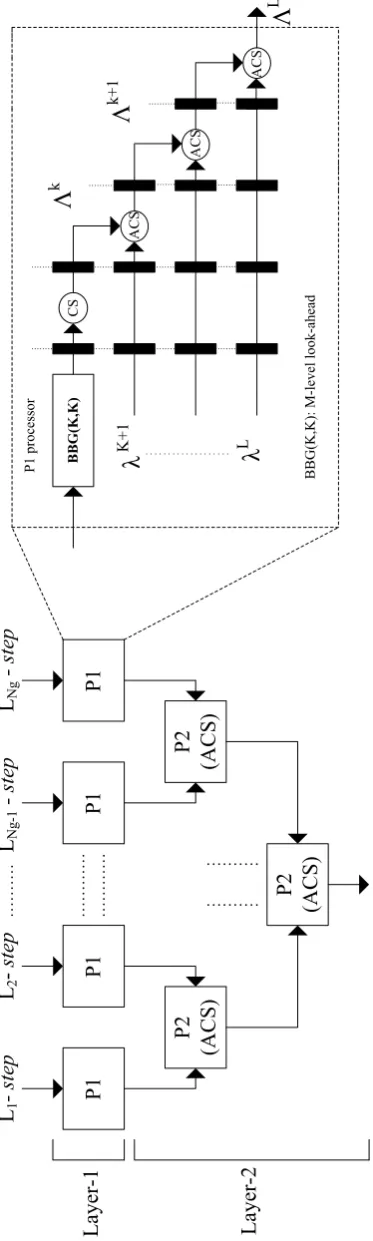
Mwhich provides less or equal latency, and also has much less complexity compared to other existing architectures [3]. For constraint lengthK and M-step look-ahead, the execution of BMP is done in a layered manner. AnM-step trellis is a bigger group consisting of MK sub-groups with a trellis ofK-step. Thus, the total numbers of P1 processors needed are MK and each P1 is responsible for computingK-step trellises. Accordingly, we have the complexities and latencies of P1 and P2 asComp.P1=N(∑ki=22i) +N2,Comp.P2=N2(N−1) +N3, and
Lat.P1,P2=K, whereN=2k−1is the number of trellis states. For P1 processors, the complex-ity of add operation isN∑ki=22iand that of the “compare” operation is N2. Similarly, for P2 processors, the complexity of add operation isN2(N−1)and that of the compare operation is
N3. For both P1 and P2 processors, the latency is same, i.e., K; however, the complexity of P2 is larger than that of P1. As the BBG approach is very efficient in computing the branch
metrics, more operations of trellis combination can be allotted into BBG-based P1 processors
in order to reduce the number of P2 processors as they are expensive in terms of complexity.
The trellis StepsL, which is computed in the P1 processors, has the constraint of being less than 2×Kin order to make sure that the latency feature is not lost. The number of groupsNg can be determined byNg=2⌊log2(MK)⌋.
The overall layered structure of the Viterbi algorithm is shown in Fig. 2.1 (in this figure,
i,j∈[1,N]and l∈[1,K]). As seen in this figure, within two layers (shown by Layer 1 and Layer 2 in Fig. 2.1), we haveNgsteps, going throughP1 andP2 processors. In eachL-level
2.3 Alternative to Look-ahead Approach 12
the final equivalent complex trellis. This figure also shows theP1 processor architecture based on the BBG algorithm. In Layer 1, although P1 leads to longer latency, as the depth of Layer
2 is reduced as well, latency penalty in not incurred.
2.3
Alternative to Look-ahead Approach
As the state nodes are connected pairwise, there are a total ofN2 connections, consisting of 2(M−K+1)parallel paths. The number of parallel paths increases exponentially with respect to
M, thereby, increasing the complexity. Generally, the exponential increase of parallel paths is avoided by a compare operation performed in each binary-trellis steps combination, thus,
the parallel paths with less metrics are always discarded. Nonetheless, each of such
add-compare operations results in a substantial amount of latency. The complexity efficiency of
look-ahead depends on constraint length of Viterbi decoder. For larger constraint lengths,
latency reduction is achieved at the expense of prohibitive computational complexity which
P 1 P 1 P 2 (ACS) P 1 P 1 P 2 (ACS) P 2 (ACS)
Layer-1 Layer
[image:23.595.208.395.111.733.2]-2 L1 -step L2 -step LNg -1 -step LNg -step BBG( K,K) CS A CS ACS ACS λ K + 1 Λ k Λ k + 1 λ L Λ L P 1 processor BBG (K ,K): M -level look -ahead
Chapter 3
Proposed Reliable Architectures
It is well-known that in different variants of concurrent error detection, either redundancy in
hardware, i.e., increase in area/power/energy consumption, e.g., through error detection codes
such as hamming codes, or redundancy in time, adding negligible area overhead at the expense
of higher total time (throughput and latency), is performed.
In this thesis, we utilize recomputing with encoded operands, where, the operations are
redone for different operands for detecting errors. During the first step, operands are applied
normally. In the recomputed step, the operands are encoded and applied and after decoding,
the correct results can be generated. Moreover, through signature-based schemes, we propose
schemes through which both transient and permanent errors can be detected.
3.1
Unified Signature-based Scheme for CSA and PCSA Units
within BMP
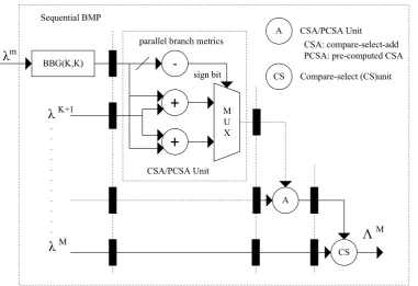
The sequential branch metric computation unit is shown in Fig. 3.1. In order to make the
ACS structure fast, parallelization of add and compare operations within the ACS itself is done
of states is doubled and the channel response is extended by an extra bit. For a complex trellis
to haveP-level parallelism, there should be 2P parallel paths for each branch. For the initial
K−1 steps, there is no compare operation, but for the remainingM−K+1 steps, the add operation is followed by a compare operation which helps in eliminating parallelism. Add and
compare operations need to be performed sequentially. For this algorithm, as seen in Fig.3.1,
the order of operations from add-compare is changed to compare-add and that is attributed as
a carry-select-add (CSA) unit. The pre-computed CSA (PCSA) is its speed-optimized variant,
the details are not presented for the sake of brevity (the PCSA architecture is preferred only
for largeKand smallMvalues).
+
+
BBG(K,K)
ȜK+1
-M U X
CSA/PCSA Unit sign bit parallel branch metrics
A
CS
ȜM ȁ
M A
CS
CSA/PCSA Unit
Compare-select (CS)unit Sequential BMP
Ȝm CSA: compare-select-add
[image:25.595.108.490.327.588.2]PCSA: pre-computed CSA
Figure 3.1: Sequential branch metric computation unit including CSA (PCSA) structures.
We utilize signature-based prediction schemes for the CSA and PCSA units. We note
that even a single stuck-at fault in such units may lead to erroneous (multi-bit) result (the
error may also propagate to the circuitry which lies ahead of the affected location, with the
3.1 Unified Signature-based Scheme for CSA and PCSA Units within BMP 16
parity, cyclic redundancy check, and the like, to name a few) are employed in our proposed
scheme for all the registers. Moreover, self-checking adders based on dual-rail encoding are
included for the adder modules.
M U X
M U X
Adder Adder P
P
P
P P
P P
Register ȁp1m(i,p) Register ȁp2m(i,p)
Register ȁp,jm
Register ȁp,km
Register ȁp1m+1(i,j) Register ȁp1m+1(i,k)
Subtractor
[image:26.595.76.521.179.611.2]CSA_Error
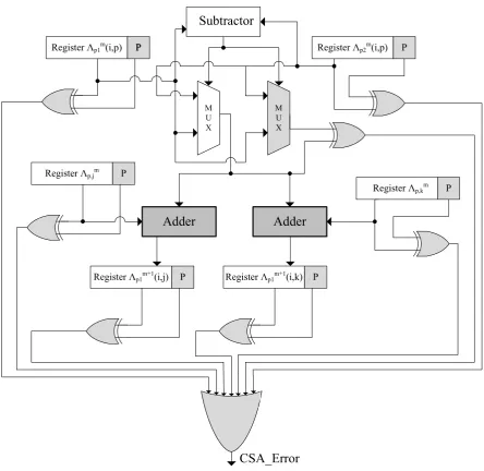
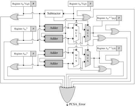
Figure 3.2: The CSA signature-based error detection approach (the shaded adders are variants
of the original ones with the proposed error detection schemes).
As shown in Figs. 3.2 and 3.3, respectively, in the CSA unit, there exists a single
the results of the original and the duplicated multiplexers are compared using an XOR gate
whose output is connected as one of the inputs to the OR gate. The input and output registers
are incorporated with additional signatures, e.g., single-bit, multiple-bit, or interleaved parity,
cyclic redundancy check, to detect faults (in figures, “P” denotes parity but it could be a
cho-sen signature based on the overhead tolerance and reliability constraints). An OR gate for the
units is required to derive the error indication flags. The OR gate raises the error indication
flags (CSA_Errorin case of the CSA unit andPCSA_Errorin case of the PCSA unit) in case an error is detected.
P P
P
P
P P
Register ȁp1m(i,p) Register ȁp2m(i,p)
Register ȁp,jm
Register ȁp,km
Subtractor
PCSA_Error Adder
Adder
M U X
M U X
Adder
Adder
M U X
M U X
P Register ȁp1m+1(p,j)
[image:27.595.76.522.301.655.2]Register ȁp1m+1(i,k)
Figure 3.3: Signature-based PCSA error detection (the shaded adders include the proposed
3.1 Unified Signature-based Scheme for CSA and PCSA Units within BMP 18
The CSA signature-based error detection approach (the shaded adders are variants of the
original ones with the proposed adders included in both CSA and PCSA units, we have used
self-checking adders as shown in Fig.3.4(some previous works include [35,36,49–52]). As
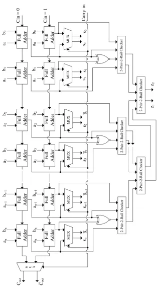
shown in this figure, the adders are cascaded to implement a self-checking adder of arbitrary
size. It consists of five two-pair two-rail checkers and also four full adders and two
multi-plexers are repeatedntimes. For the normal operation, no additional delay has resulted due to self-checking feature. The checker has two pairs of inputs driven in such a way that in the
fault free scenario, the outputs are equal pairwise. This is performed using XNOR gates and
appropriate connections. There are two outputs from the checker and the outputs are also in
two-rail form as the inputs. Even if one of the inputs of the checker has a fault, the output is
not in two-rail form and, thus, an error indication flag is raised to indicate that a fault has been
M U X F u ll A d d er F u ll A d d er F u ll A d d er F u ll A d d er M U X M U X 2 -P ai r- 2-R ai l C he ck er an bn an-1
bn-1
an bn an-1 bn-1
sࡄn
sn
sn-1
sࡄn-1
F u ll A d d er F u ll A d d er F u ll A d d er F u ll A d d er M U X M U X 2 -P ai r- 2-R ai l C he ck er a3 b3 a2 b2 a3 b3 a2 b2
sࡄ3
s3
s2
sࡄ2
F u ll A d d er F u ll A d d er F u ll A d d er F u ll A d d er M U X M U X 2- Pair-2-Ra il Che cker a1 b1 a0 b0 a1 b1 a0 b0
sࡄ1
s1
s0 sࡄ0
2-P air -2-Rail C hecke r 2-P air -2-Rail C hecke r z1 z2 Co u t C
ࡄout
[image:29.595.142.456.104.679.2]C in = 0 C in = 1 C ar ry -i n
3.1 Unified Signature-based Scheme for CSA and PCSA Units within BMP 20
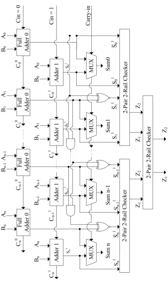
The adders as shown in Fig.3.5can also be implemented in both CSA and PCSA designs
using the modified self-checking adder [53].In this variant, twon-bit ripple carry adders are used to precompute the sum bits with complemented values of carry-in, i.e., 0 and 1, and the
original value of carry-in is used to select the actual sum bits. We employ this new adder [24]
in the architectures and evaluate its performance and efficiency. Fig. 3.5 shows the design
module of this variant for self-checking carry-select adder; the area overhead of which is
found to be in the range of 20%-35% based on the input bit-size. An important modification
done in this new adder is the inputs given to the two-pair two-rail checker. For carrying out the
A d d er 1 A d d er 1 A d d er 1 A d d er 1 2 -P ai r 2 -R ai l C h ec k er 2 -P ai r 2 -R ai l C h ec k er 2 -P ai r 2 -R ai l C h ec k er M U X M U X M U X M U X F u ll A d d er 0 F u ll A d d er 0 F u ll A d d er 0 F u ll A d d er 0 C ar ry -i n C in = 1 C in = 0 A0 A1 An -1 An B0 B1 Bn -1 Bn C0 0 C1 0 Cn -1 0 Cn 0 A0 B0 A1 B1 C0 1 C1 1 Cn -1 1 Cn 1 S u m 0 S u m 1 S u m n -1 S u m n Z1 Z2 Z1 Z2 Sn 1 S ࡄn 1 Sn -1 1 S
ࡄn-1
1 S1 1 S ࡄ1 1 S0 1 S ࡄ0 1 Sn 1
Sn-1
[image:31.595.126.471.105.682.2]1 S1 1 S0 1 Z1 Z2 Bn -1 An -1 Bn An
3.2 Recomputing with Encoded Operands for CSA and PCSA 22
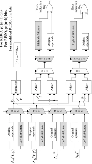
3.2
Recomputing with Encoded Operands for CSA and PCSA
In this section, the error detection CSA and PCSA architectures are designed through
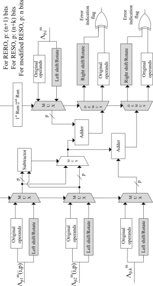
recom-puting with encoded operands, e.g., RERO, RESO, and variants of RESO, as shown in Figs.
3.6 and3.7 with the locations of error detection modules shaded. Since this approach takes
more number of cycles for completion, to alleviate the throughput degradation, the
architec-ture is pipelined in the following fashion. First, pipeline registers are added to sub-pipeline
the architectures, assisting in dividing the timing into sub-parts. The original operands are fed
in during the first cycle. Nonetheless, during the second cycle, the second half of the circuit
M U X M U X M U X
Adder
Adder
D E M U X
1 st Run /2 nd Run Right shift /Rotate Right shift /Rotate
D E M U X
M U X
Subtractor
Original operands Original operands
Left shift /Rotate Left shift /Rotate Left shift /Rotate
Original operands Original operands Original operands
Λp1
m (i,p)
Λp2
m (i,p) Λ
p,k
m
p p
Original ope
rands
M U X
[image:33.595.149.449.115.673.2]L eft shift/Rotate Error indication flag Λp,j m p p F or RERO, p: (n +1) bits For RESO, p: (n+k) bits For modified RESO , p: n bits Error indication flag
3.2 Recomputing with Encoded Operands for CSA and PCSA 24
For the CSA and PCSA architectures in Figs. 3.6 and 3.7, we also employ RESO and a
RESO variant scheme for fault diagnosis. Both CSA and PCSA units consist of four inputs,
each of them are passed in its original form and in the left shifted or rotated form to one of
the multiplexers. If the select lines of these multiplexers are set to the first run, the original
operands are passed without any change. If these are set to second run, the second (modified,
i.e., left shifted/rotated) operands are passed. For the CSA unit, the inputs are fed to the
subtractor and also to the multiplexer whose select line is set by the comparator. This serves
as the design of compare-select unit. The output of the multiplexer is replicated and asserted
as one of the inputs to two adders included in the design. The outputs of both of the adders are
the outputs of the CSA unit. These are passed through the demultiplexers and the outputs of
the demultiplexers are compared using an XOR gate, and the error indication flag is raised in
case of an error. For the PCSA unit, the first two inputs are fed to the comparator which acts
as the select line for the two multiplexers driven by the four adders used in the design. The
other two inputs in combination with the previous inputs are given to the adders. The outputs
of the two multiplexers are the outputs of the PCSA unit and to ensure that they are error-free,
M U X M U X M U X M U X
Adder Adder
M U X D E M U X
1 st Run /2 nd Run Right shift /Rotate Right shift /Rotate
D E M U X
M U X
Subtractor Adder
Original operands Original operands
Left shift/ Rotate Left shift/ Rotate Left shift/ Rotate Left shift/ Rotate
Original operands Original operands Original operands Original operands
Λ
p1m
(i,p)
Λ
p2m
(i,p)
Λ
p,jm
Λ
p,k m p p p p AdderFor
RERO
,
p:
(n+1)
bits
F
or
RESO,
p:
(n+k)
bits
For
modified
RESO
,
p:
n
bits
Error indicationflag Error
indication
[image:35.595.145.459.115.672.2]flag
3.2 Recomputing with Encoded Operands for CSA and PCSA 26
We have utilized RESO which performs the recomputation step with shifted operands, i.e.,
all operands are shifted left or right bykbits (this method is efficient in detectingkconsecutive logic errors andk−1 arithmetic errors). For CSA and PCSA architectures in Figs. 3.6 and 3.7, let us assume g(x,y) is the result of the operation which is stored in a register. The same operation is performed again withxandy shifted by certain number of bits. This new result g′(x,y) is stored and the original result g(x,y) can be obtained by shifting g′(x,y) in the opposite direction. Another used method in the proposed scheme is a modified version
of the RESO scheme and this modification is that the bits that shift out are not preserved.
This signifies that the total number of bits required for operation is only “n” bits and, hence, becomes more advantageous in terms of hardware cost than RESO and RERO methods, as
pointed out in Figs. 3.6and3.7. In modified RESO, only (n−k) LSBs ofg(x)are compared with the shifted (n−k) LSBs ofg′(x). This approach is a compromise between the area/power consumption and the error coverage.
In order to execute the RERO method, we have added low hardware overhead to the initial
design. RERO is used for detecting errors concurrently in the arithmetic units. Considering
two n-bit rotations R and R−1, suppose the input to an arithmetic function is x and g(x) is the output such thatg(x) =R−1×(g(R(x))). The result ofg(x) computation happens to be the result of first run and R−1×(g(R(x))) computation happens to be the second run. For both the CSA and PCSA units, we have used the RERO scheme in Figs. 3.6 and 3.7. The
first challenge in RERO for in Figs. 3.6and3.7 is to avoid the interaction between the MSB
and LSB of the original operand during the recomputation operation. The second challenge
in RERO for CSA and PCSA architectures is to ensure performance enhancements through
sub-pipelining to increase the frequency and alleviate the throughput overhead as part of the
FPGA and ASIC implementations. Finally, let us present a general approach for alleviating
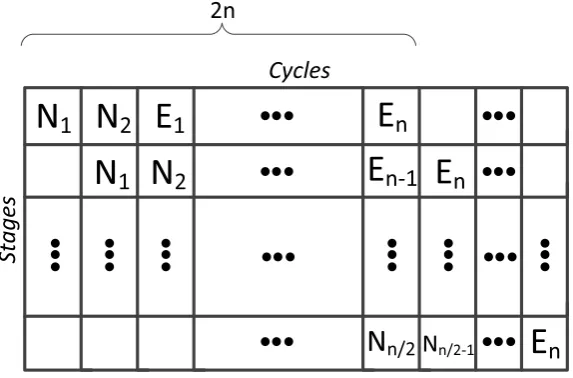
the throughput degradations of the proposed schemes. Suppose a number of pipeline registers
segments of the pipelined stages by∆1-∆n. In a typical assertion, the original input can be first
applied (to∆1) and in the second cycle, while the second half (∆2) of the architecture executes
the first input, the encoded variant of the first input is fed. This trend can be scaled tonstages for normal (N) and encoded (E) operands.
N
2E
1N
1N
2E
nE
n-1E
nStages
Cycles
E
n 2nN
1 [image:37.595.155.442.212.401.2]N
n/2Nn/2-1Figure 3.8: Compromise in asserting the encoded operands (can be tailored based on reliability
constraints).
We have shown in Fig. 3.8an approach based on which a compromise for the assertions
is performed. Depending on the requirements, one can fulfill various reliability constraints.
As seen in Fig. 3.8, a number of cycles are considered with the normal operands shown by
N1−Nnand the encoded operands shown byE1−En. Let us assume thatN1is asserted at the beginning (first stage and first cycle). We have a number of options in the second cycle, e.g.,
asserting the second normal operand (N2)or the first encoded operand (encoded variant ofN1
which isE1). Fig.3.8shows the former option as an example. In the third cycle, many options exist, among which assertingE1has been chosen to depict in Fig. 10. This trend continues and after 2ncycles, one has En,En−1, ...,Nn/2 as the entries to various stages. Such an approach ensures lower degradation in the throughput at the expense of more area overhead and can be
Chapter 4
Benchmarks and Assessments
In what follows, we present the results of our error simulations. Then, both ASIC and FPGA
implementation results are presented for benchmark.
4.1
Simulations for Fault Injection Models
The fault coverage of the proposed architectures has been assessed by subjecting them to a
fault model which considers permanent, transient, and single/multiple-bit stuck-at faults. The
proposed error detection schemes are capable of detecting both permanent and transient faults.
We inject faults at different locations and monitor the error indication flags. The fault model
applied for evaluating the proposed error schemes has been realized through linear feedback
shift registers (LFSRs) to generate pseudo-random test patterns.
For single stuck-at faults for signature-based schemes of CSA and PCSA blocks, the
cov-erage is 100 percent (which can be analytically proved as well) and simulations are performed
extensively to confirm that. In the signature-based schemes of CSA and PCSA blocks,
perma-nent and transient faults can be detected and the blocks predicting the signatures are included
in different sub-parts of the architecture. For multiple stuck-at faults, the fault coverage
Table 4.1: Area, delay, and power consumption benchmark on ASIC for CSA architecture. Architecture Area (µm2) Gate equi. (GE) Delay (ns) Power (µW) Area over. Delay over. Power over.
CSA 486.17 319 1.24 90.64 - -
-CSA_RESO (+ 2 bits) 603.84 396 1.51 98.60 24.20% 21.77% 8.78%
CSA_RERO (+1 bit) 547.17 359 1.26 91.04 12.55% 1.61% 0.44%
CSA_M_RESO 488.66 320 1.26 90.89 0.51% 1.61% 0.28%
For RERO, RESO, and modified RESO, the architectures of CSA and PCSA require two
runs for detecting transient and permanent faults. The simulation results obtained show that for
RESO, 99.612% fault coverage is obtained for 99,675 injected faults for CSA, and 99.740%
fault coverage for 99,727 injected faults for PCSA. Moreover, for RERO, the fault coverage is
99.861% for 99,724 injected faults for CSA, and 99.901% for 99,742 injected faults for PCSA.
Lastly, for modified RESO, the fault coverage of 99.485% is obtained for 99,779 injected
faults for CSA, and 99.631% is the fault coverage for 99,679 injected faults for PCSA. In the
following section, it is shown that such fault coverage is at the expense of acceptable overheads
on ASIC and FPGA platforms.
4.2
ASIC and FPGA Implementations
We present the ASIC implementation results for TSMC 32-nm library and the FPGA
imple-mentation results for Virtex-6 family (xc6vlx75t-3ff484 device) using Xilinx ISE 14.7.
For ASIC, we use Synopsys Design Compiler, and all the design constraints are set the
same for different architectures for fair comparison. Moreover, medium map and optimization
efforts are used for all the designs. The overhead results for ASIC are obtained for of the
area [µm2], the NAND-gate equivalency (denoted as gate equivalent [GE] and used as the
architecture area over that of a two-input NAND gate in 32nm TSMC which is 1.524864
µm2), the delay (ns), the power consumption (µW) at the typical chosen frequency of 50
MHz, the throughput (Gbps), and the efficiency (which is defined as the throughput over area, i.e.,Gbps/µm2).
architec-4.2 ASIC and FPGA Implementations 30
Table 4.2: PCSA area, delay, and power consumption benchmark on ASIC.
Architecture Area (µm2) Gate equi. (GE) Delay (ns) Power (µW) Area over. Delay over. Power over.
PCSA 590.8 387 0.85 88.99 - -
-PCSA_RESO (+ 2 bits) 731.6 480 1.01 109.54 23.83% 19.39% 23.09%
PCSA_RERO (+ 1 bit) 661.7 434 0.93 100.86 12.00% 9.93% 13.34%
PCSA_M_RESO 594.7 390 0.87 89.88 0.66% 2.25% 1.00%
Table 4.3: CSA benchmark through Xilinx Virtex-6 (xc6vlx75t-3ff484 device) FPGA family. Architecture Slices Delay (ns) Slice overhead Delay overhead
CSA 14 0.79 -
-CSA_RESO 16 0.89 14.29% 12.52%
CSA_RERO 16 0.85 14.29% 7.46%
CSA_M_RESO 14 0.80 negligible 1.14%
tures. The overhead evaluation for FPGA are obtained for of the area (in terms of number of
occupied slices, knowing that slice registers and look-up tables are within), the delay (ns), the throughput (Gbps), and the efficiency (Gbpsover the number of occupied slices).
The architectures have been designed with the design entry Verilog HDL. The
implemen-tations have been carried out for the original architectures as well as error detection schemes.
The results of our benchmark on FPGA and ASIC are presented in Tables4.1, 4.2, 4.3, 4.4,
4.5,4.6.
As seen in Tables4.1and4.2, ASIC benchmark results for CSA and PCSA are presented
for the original architectures, RESO with two bits [CSA_RESO (+ 2 bits) and PCSA_RESO
(+ 2 bits)], RERO [CSA_RERO (+1 bit) and PCSA_RERO (+1 bit)], modified variant of
RESO in which no additional bit is added [CSA_M_RESO and PCSA_M_RESO], and also
for signature-based architectures [CSA_S and PCSA_S]. RESO has higher overheads (still at
most 24.20%) compared to RERO and modified RESO variants which have 12.55% [0.51%],
1.61% [1.37%], 0.44% [0.28%] (for area, delay, and power consumption of CSA) and 12.00%
[0.66%], 9.93% [2.25%], 13.34% [1.00%] (for area, delay, and power consumption of PCSA).
It is noted that for signature-based CSA, based on the summations of total two-rail checkers
(two), we have also derived the area overhead of 17.67%, the delay overhead of 2.02%, and
Table 4.4: Xilinx Virtex-6 FPGA implementations for PCSA. Architecture Slices Delay (ns) Slice overhead Delay overhead
PCSA 14 0.82 -
-PCSA_RESO 19 0.92 35.71% 12.18%
PCSA_RERO 19 0.90 35.71% 9.62%
[image:41.595.74.523.249.351.2]PCSA_M_RESO 14 0.83 negligible 1.10%
Table 4.5: Throughput, efficiency, and energy consumption benchmark on ASIC for CSA and PCSA.
Architecture Throughput (Gbps) Efficiency (Mbpsµm2) Energy (f J) Throughput deg. Efficiency deg. Energy over.
CSA 6.45 14.0 112.4 - -
-CSA_RESO (+ 2 bits) 5.30 8.7 148.8 17.83% 37.8% 32.1%
CSA_RERO (+1 bit) 6.35 11.6 114.7 1.55% 17.1% 2.1%
CSA_M_RESO 6.35 13.0 114.5 1.55% 7.1% 2.0%
PCSA 9.41 15.9 76.5 - -
-PCSA_RESO (+ 2 bits) 7.92 10.8 110.1 15.80% 32.1% 44%
PCSA_RERO (+1 bit) 8.60 13.0 93.1 8.61% 18.2% 22%
PCSA_M_RESO 9.19 15.5 78.3 2.33% 2.5% 3%
of PCSA, which takes into account four checkers, the area overhead of 21.49%, the delay
overhead of 15.57%, and the power consumption overhead of 13.62% are achieved.
Tables 4.3 and 4.4 show the results of our FPGA implementations for CSA and PCSA.
Similar to the ASIC results, we get lower overheads for RERO and modified RESO for
the FPGA implementations, i.e., 14.29% [negligible] and 7.46% [1.14%] (for area and
de-lay of CSA) and 35.71% [negligible] and 9.62% [1.10%] (for area and dede-lay of PCSA). For
signature-based CSA, we have also derived the area overhead of 14.89% and the delay
over-head of 2.78%. Moreover, for the signature-based scheme of PCSA, the area overover-head of
29.79% and the delay overhead of 1.58% are achieved.
Table4.5 shows the throughput, efficiency, and energy benchmark on ASIC for CSA and
PCSA. It can be observed that RESO (CSA and PCSA) has higher energy and throughput
over-heads, i.e., 37.8% [32.1%] and 17.83% [15.80%] (for efficiency and throughput). The
modi-fied RESO (CSA and PCSA) demonstrates the lowest overheads for efficiency and throughput,
i.e., 7.1% [2.5%] and 1.55% [2.33%] (for efficiency and throughput). Table4.6represents the
bench-4.2 ASIC and FPGA Implementations 32
Table 4.6: Xilinx Virtex-6 FPGA implementations for throughput and efficiency benchmark for CSA and PCSA.
Architecture Throughput (Gbps) [over.] Efficiency (#MbpsSlice) [over.]
CSA 10.1 721
CSA_RESO 8.9 [10.9%] 561 [22.2%]
CSA_RERO 9.4 [6.9%] 588 [18.4%]
CSA_M_RESO 10.0 [1.0%] 714 [2.4%]
PCSA 9.7 692
PCSA_RESO 8.7 [10.3%] 457 [33.9%]
PCSA_RERO 8.8 [9.3%] 467 [32.5%]
PCSA_M_RESO 9.6 [1.0%] 687 [0.7%]
markresults,theoverheadsobtainedforRESO(CSAandPCSA)areslightlyhigh,i.e.,22.2%
[33.9%] and 10.9% [10.3%] (for efficiency and throughput)and lowest for modified RESO
(CSAandPCSA),i.e.,2.4%[0.7%]and1%[1%](forefficiencyandthroughput).
Conclusions
In this thesis, we presented fault diagnosis models for the CSA and PCSA units of
low-complexity and low-latency Viterbi decoder. The simulation results for the proposed
meth-ods of RESO, RERO, modified RESO, parity and self-checking adder based designs for both
CSA and PCSA units show very high fault coverage (almost 100 percent) for the randomly
distributed injected faults. The proposed architectures has been successfully implemented on
Xilinx Virtex-6 Family and also by using the 32nm library using Synopsys Design Compiler
for the ASIC implementation. Also, the ASIC and FPGA implementation results show that
overheads obtained are acceptable. Thus the proposed models are reliable and efficient.
5.1
Future Work
This thesis work focussed on performing the fault detection on the CSA unit and the PCSA
unit. The work can be extended by performing fault detection for the different binary-trellis
groups using the parity registers and duplicating the adders.
Recomputing with encoded operands and unified signature-based scheme were used to
detect faults in this work. In future, the proposed architectures can be tested with other fault
References
[1] A. J. Viterbi, “Error bounds for convolutional codes and an asymptotically optimum
decoding algorithm,”IEEE Trans. Inf. Theory, vol. 13, no. 2, pp. 260 – 269, 1967. [2] S. Ranpara and D. S. Ha, “A low-power Viterbi decoder design for wireless
commu-nications applications,” IEEE Intl. Conf. Proceedings ASIC/SOC, pp. 377 – 381, Sep. 1999.
[3] R. Liu and K. Parhi, “Low-latency low-complexity architectures for Viterbi decoders,”
IEEE Trans. Circuits Syst. I, Reg. Papers, vol. 56, no. 10, pp. 2315 – 2324, 2009.
[4] H. Liu, Z. Wang, X. Huang, K. Z. Liu, Z. Wang, X. Huang, and K. Zhang, “High-speed
low-power Viterbi decoder design for tcm decoders,” IEEE Trans. VLSI Syst., vol. 20, no. 4, pp. 755–759, Apr 2012.
[5] K. Cholan, “Design and implementation of low power high speed Viterbi decoder,” in
Proc. Int. Conf. on Communications Technology and System, vol. 30, 2011, pp. 61–68. [6] P. Black, P. Alto, and H. Meng, “A 1-Gb/s, four-state, sliding block Viterbi decoder,”
IEEE J. Solid-State Circuits, vol. 32, pp. 797 – 805, 1997.
[7] L. Horng-Dar and D. Messerschmitt, “Algorithms and architectures for concurrent
[8] K. Arunlal and S. Hariprasad, “An efficient Viterbi decoder,”Int. Journal of Advanced Information Technology, vol. 2, no. 1, Feb 2012.
[9] J. Kong and K. Parhi, “K-nested layered look-ahead method and architectures for high
throughput Viterbi decoder,” in Proc. IEEE Workshop on Signal Processing Systems, 2003, pp. 99 – 104.
[10] G. Jung, J. Kong, G. Sobelman, and K.Parhi, “High-speed add-compare-select units
us-ing locally self-resettus-ing CMOS,” inIEEE Int. Symp.Circuits and Systems, vol. 1, 2002, pp. 889–892.
[11] K. K. Parhi,VLSI Digital Signal Processing Systems: Design and Implementation. Wi-ley, 1999.
[12] G. Fettweis and H. Meyr, “Parallel Viterbi algorithm implementation: Breaking the
ACS-bottleneck,”IEEE Trans. Commun., vol. 37, no. 8, pp. 785 – 790, 1989.
[13] V. Gierenz, O. Weiss, T. Noll, I. Carew, J. Ashley, and R. Karabed, “A 550 Mb/s radix-4
bit-level pipelined 16-state 0.25-um CMOS Viterbi decoder,” in Proc. IEEE Int. Conf. Appl.-Specific Syst., Archit. Process, 2000, pp. 195 – 201.
[14] P. Black and T. H. Meng, “A 140-Mb/s, 32-state, radix-4 Viterbi decoder,”IEEE J. Solid-State Circuits, vol. 27, no. 12, pp. 1877 – 1885, 1992.
[15] T. Gemmeke, M. Gansen, and T. Noll, “Implementation of scalable power and area
effi-cient high-throughput Viterbi decoders,”IEEE J. Solid-State Circuits, vol. 37, no. 7, pp. 941 – 948, 2002.
[16] A. Yeung and J. Rabaey, “A 210 Mb/s radix-4 bit-level pipelined Viterbi decoder,” in
References 36
[17] K. Parhi, “An improved pipelined MSB-first add-compare select unit structure for Viterbi
decoders,”IEEE Trans. Circuits Syst. I, Reg. Papers, vol. 51, no. 3, pp. 504 – 511, 2004. [18] K. Parhi and J. J. Kong, “Low-latency architectures for high-throughput rate Viterbi
de-coders,”IEEE Trans. Very Large Scale Integr. (VLSI) Syst., vol. 12, no. 6, pp. 642 – 651, 2004.
[19] H. Bar-El, H. Choukri, D. Naccache, and M. Tunstall, “The sorcerer’s apprentice guide
to fault attacks,”IEEE Proceedings, vol. 94, no. 2, pp. 370 – 382, Jan 2006.
[20] M. Karpovsky and A. Taubin, “New class of nonlinear systematic error detecting codes,”
IEEE Trans. Information Theory, vol. 50, no. 8, pp. 1818 – 1819, July 2004.
[21] M. Karpovsky, K. Kulikowski, and A. Taubin, Differential Fault Analysis Attack Re-sistant Architectures for the Advanced Encryption Standard, ser. 153, Y. D. A. K. J. Quisquater, P. Paradinas, Ed. Springer US, 2004, no. 4.
[22] M. Karpovsky, K. Kulikowski, and Z. Wang, “Robust error detection in communication
and computational channels,” inInt. Workshop on Spectral Techniques, 2007.
[23] D. Vasudevan, P. Lala, and J. Parkerson, “Self-checking carry-select adder design based
on two-rail encoding,”IEEE Trans. Circuits Syst. I, Reg. Papers, vol. 54, no. 12, pp. 2696 – 2705, Dec. 2007.
[24] M. Akbar and J.-A. Lee, “Comments on "self-checking carry-select adder design based
on two-rail encoding",”IEEE Trans. Circuits Syst. I, Reg. Papers, vol. 61, no. 7, pp. 2212 – 2214, July 2014.
[26] C.-H. Yen and B.-F. Wu, “Simple error detection methods for hardware implementation
of Advanced Encryption Standard,”IEEE Trans. Comput., vol. 55, no. 6, pp. 720 – 731, 2006.
[27] T. G. Malkin, F. Standaert, and M. Yung, “A comparative cost/security analysis of fault
attack countermeasures,” inProc. Int. Workshop, Fault Diagnosis and Tolerance in Cryp-tography, 2006, pp. 159–172.
[28] M. Mozaffari-Kermani, R. Azarderakhsh, and A. Aghaie, “Reliable and error detection
architectures of Pomaranch for false-alarm-sensitive cryptographic applications,”IEEE Trans. Very Large Scale Integr. (VLSI) Syst., 2015, to appear.
[29] G. D. Natale, M. Doulcier, M. Flottes, and B. Rouzeyre, “A reliable architecture for the
Advanced Encryption Standard,” inProc. IEEE European Test Symp., 2008, pp. 13 – 18. [30] M. Mozaffari-Kermani and A. Reyhani-Masoleh, “Concurrent structure-independent
fault detection schemes for the Advanced Encryption Standard,” IEEE Trans. Comput., vol. 59, no. 5, pp. 608 – 622, 2010.
[31] M. Mozaffari-Kermani and A. Reyhani-Masoleh, “Efficient fault diagnosis schemes for
reliable lightweight cryptographic ISO/IEC standard CLEFIA benchmarked on ASIC
and FPGA,”IEEE Trans. Ind. Electron., vol. 60, no. 12, pp. 5925 – 5932, 2013.
[32] P. Maistri and R. Leveugle, “Double-data-rate computation as a counter measure against
fault analysis,”IEEE Trans. Comput., vol. 57, no. 11, pp. 1528 – 1539, 2008.
[33] G. Bertoni, L. Breveglieri, I. Koren, P. Maistri, and V. Piuri, “A parity code based fault
References 38
[34] M. Mozaffari Kermani, R. Azarderakhsh, C. Lee, and S. Bayat-Sarmadi, “Reliable
concurrent error detection architectures for extended Euclidean-based division over
GF(2m),” IEEE Trans. Very Large Scale Integr. (VLSI) Syst., vol. 61, no. 2, pp. 995 – 1003, 2014.
[35] K. Kulikowski, Z. Wang, and M. Karpovsky, “Comparative analysis of robust fault attack
resistant architectures for public and private cryptosystems,” inProc. Int. Workshop Fault Diagnosis Tolerance Cryptography, 2008, pp. 41 – 50.
[36] M. Mozaffari-Kermani, K. Tian, R. Azarderakhsh, and S. Bayat-Sarmadi,
“Fault-resilient lightweight cryptographic block ciphers for secure embedded systems,” IEEE Embed. Systems Lett., vol. 6, no. 4, pp. 89–92, 2014.
[37] L. Breveglier, I. Koren, and P. Maistri, “An operation-centered approach to fault detection
in symmetric cryptography ciphers,” IEEE Trans. Computers, vol. 56, no. 5, pp. 635 – 649, March 2007.
[38] A. Aysu, E. Gulcan, and P. Schaumont, “Simon says: Break area records of block ciphers
on fpgas,”IEEE Embedded Systems Letters, vol. 6, no. 2, pp. 37 – 40, May 2014. [39] A. Tenca and M. Ercegovac, “A variable long-precision arithmetic unit design for
recon-figurable coprocessor architectures,” inProc. IEEE Symp. FPGAs for Custom Computing Machines, April 1998, pp. 216 – 225.
[40] M. Ercegovac and T. Lang, Division by digit recurrence in Digital Arithmetic. San Francisco: D.E.M Penrose.
[41] G. Xiaofei and R. Karri, “Recomputing with permuted operands: A concurrent error
[42] B. Johnson, J. Aylor, and H. Hana, “Efficient use of time and hardware redundancy for
concurrent error detection in a 32-bit VLSI adder,”IEEE J. Solid-State Circuits, vol. 23, no. 1, pp. 208 – 215, Feb. 1988.
[43] H. Garner, “Error codes for arithmetic operations,”IEEE Trans. on Electronic Comput-ers, vol. 15, no. 5, pp. 763 – 770, Oct. 1966.
[44] S. Durand and C. Piguet, “FPGA with selfrepair capabilities,” Int. Workshop on Field Programmable Gate Arrays.
[45] M. Berg and M. Greenbelt, “Fault tolerance implementation within SRAM based FPGA
designs based upon the increased level of single event upset susceptibility,” IEEE Int. Symp. On-Line Testing, no. 12, 2006.
[46] J. Emmert, C. Stroud, and M. Abramovici, “Online fault tolerance for FPGA logic
blocks,” IEEE Trans. Very Large Scale Integr. (VLSI) Syst., vol. 15, no. 2, pp. 216 – 226, Feb. 2007.
[47] J. Patel and L. Fung, “Concurrent error detection in ALUs by recomputing with shifted
operands,”IEEE Trans. Comput., vol. C-31, no. 7, pp. 589 – 595, 1982.
[48] J. Li and E. Swartzlander, “Concurrent error detection in ALUs by recomputing with
rotated operands,” in Proc. IEEE Int. Workshop Defect and Fault Tolerance in VLSI Systems, 1992, pp. 109 – 116.
[49] T. Jamil, “An introduction to complex binary number system,” inProc. IEEE Int. Conf. Inform. Comput., 2011, pp. 229 – 232.
References 40
[51] S. Mozafari, M. Fazeli, S. Hessabi, and S. Miremadi, “A low cost circuit level fault
detection technique to full adder design,” in Proc. IEEE Int. Conf. Electron., Circuits and Syst. (ICECS), 2011, pp. 446 – 450.
[52] F. Shih, “High performance self-checking adder for VLSI processor,” in Proc. IEEE Custom Integr. Circuits Conf, 1991, pp. 15.7/1 – 15.7/3.
[53] L. Vos, R. Jain, H. D. Man, and W. Ulbrich, “A fast adder-based multiplication unit for
customised digital signal processors,” in Proc. IEEE Int. Conf. Acoustics, Speech, and Signal Proc., vol. 11, April 1986, pp. 2163 – 2166.
[54] M. Mozaffari Kermani and R. Azarderakhsh, "Reliable hash trees for post-quantum stateless cryptographic hash-based signatures," in Proc. IEEE Int. Symp. Defect and Fault Tolerance in VLSI Systems (DFT), pp. -, Oct. 2015.
[55] M. Mozaffari Kermani and A. Reyhani-Masoleh, "Reliable Hardware Architectures for the Third-Round SHA-3 Finalist Grostl Benchmarked on FPGA Platform," in Proc. IEEE Int. Symp. Defect and Fault Tolerance in VLSI Systems (DFT), pp. 325-331, Vancouver, Canada, Oct. 2011.
[56] M. Mozaffari Kermani and A. Reyhani-Masoleh, "A High-Performance Fault Diagnosis Approach for the AES SubBytes Utilizing Mixed Bases," in Proc. IEEE Workshop Fault Diagnosis and Tolerance in Cryptography (FDTC), pp. 80-87, Nara, Japan, Sep. 2011. [57] M. Mozaffari Kermani and A. Reyhani-Masoleh, "A Lightweight Concurrent Fault Detection Scheme for the AES S-Boxes Using Normal Basis," in Proc. LNCS Cryptographic Hardware and Embedded Systems (CHES), pp. 113-129, Washington, D.C., USA, Aug. 2008 [58] M. Mozaffari Kermani and A. Reyhani-Masoleh, "A Structure-independent Approach for Fault Detection Hardware Implementations of the Advanced Encryption Standard," in
Proc. IEEE Workshop Fault Diagnosis and Tolerance in Cryptography (FDTC), pp. 47-53, Vienna, Austria, Sep. 2007.
2006.
[59] M. Mozaffari Kermani and A. Reyhani-Masoleh, "Parity-based Fault Detection Architecture of S-box for Advanced Encryption Standard," in Proc. IEEE Int. Symp. Defect
and Fault Tolerance in VLSI Systems (DFT), pp. 572-580, Washington, D.C., USA, Oct.
2006.
[60] M. Mozaffari Kermani and A. Reyhani-Masoleh, "Parity Prediction of S-box for AES,"
in Proc. IEEE Canadian Conference on Electrical and Computer Engineering (CCECE), pp.
2357-2360, Ottawa, Canada, May 2006.
[61] M. Mozaffari Kermani, N. Manoharan, and R. Azarderakhsh, "Reliable radix-4
complex division for fault-sensitive applications," IEEE Trans. Comput.-Aided Design Integr.
Circuits Syst., vol. 34, no. 4, pp. 656-667, Apr. 2015.
[62] S. Bayat-Sarmadi, M. Mozaffari Kermani, and A. Reyhani-Masoleh, "Efficient and concurrent reliable realization of the secure cryptographic SHA-3 algorithm,"
IEEE Trans. Comput.-Aided Design Integr. Circuits Syst., vol. 33, no. 7, pp. 1105-1109,
Jul. 2014.
[63] M. Mozaffari Kermani and A. Reyhani-Masoleh, "A Low-Power High-Performance Concurrent Fault Detection Approach for the Composite Field S-box
and Inverse S-box," IEEE Trans. Comput., vol. 60, no. 9, pp. 1327-1340, Sep. 2011.
[64] M. Mozaffari Kermani and A. Reyhani-Masoleh, "A Lightweight High-Performance Fault Detection Scheme for the Advanced Encryption Standard
Using Composite Fields," IEEE Trans. Very Large Scale Integr. (VLSI) Syst., vol. 19, no. 1, pp. 85-91, Jan. 2011.
[65] M. Mozaffari Kermani, "Fault Detection Schemes for High Performance VLSI
Implementations of the Advanced Encryption Standard", M.E.SC. Thesis, The University of Western Ontario.
[66] M. Mozaffari-Kermani, "Reliable and High-Performance Hardware Architectures for the Advanced Encryption Standard/Galois Counter Mode," Ph.D. Thesis, University of Western Ontario.