CMOS VLSI Correlator Design for
Radio-Astronomical Signal Processing
A thesis presented in partial fulfilment of the requirements for the
degree of
Doctor of Philosophy
in
Engineering
at Massey University, Auckland, New Zealand
Acknowledgements
I would like to acknowledge my supervisor Rezaul Hasan without whose support this work would not have been possible.
Abstract ii
Acknowledgements iii
List of figures ix
List of tables x
List of acronyms and abbreviations xi
1 Introduction 1
1.1 Telescopes with multiple antennas 1
1.2 The correlator 2
1.3 Motivation 3
1.4 Thesis outline 4
2 Digital CMAC design 6
2.1 Complex multiplication and CMAC 6
2.2 CMAC multiplier design 8
2.3 Design of digital circuit cells 9
2.3.1 Adder circuits 11
2.3.2 Memory registers 15
2.4 CMAC implementation 17
3 Multiple-accumulator CMACs for the input-buffered FX correlator 21
3.1 Architecture overview 21
3.2 Grouping SIs for multiple-accumulator CMACs 23
3.3 Quantifying memory access improvements 25
3.4 Design and evaluation of multiple-accumulator CMACs 27
3.5 Conclusion 29
4 DET flip-flops based on C-elements 30
4.1 Low-glitch LG_C flip-flop 31
4.2 Implicit-pulsed IP_C flip-flop 33
4.3 Floating-node FN_C flip-flop 34
4.4 Conditional-toggle CT_C and CTF_C flip-flops 37
4.5 Simulation methodology 39
4.6 Simulation results and comparison 44
Contents
5 Memory design for the output-buffered FX correlator 49
5.1 Sequential access memory 50
5.2 Design description 52
5.3 Testing setup 54
5.4 Test results 56
5.5 Conclusion 59
6 SerDes I/O design 62
6.1 Analog design 62
6.2 LVDS clock reference receiver 63
6.3 Phased-locked loop design 64
6.4 Serialiser 64
6.5 Scrambler 66
6.6 Predriver 66
6.7 Output driver 70
6.7.1 Feed-forward equaliser 70
6.7.2 Impedance tuning 71
6.7.3 ESD protection 71
6.8 Driver biasing 71
6.9 Conclusion 76
7 Conclusion 77
7.1 Summary 77
7.2 Suggestions for future work 78
Bibliography 79
A CMAC multiplier netlists 87
A.1 4-bit CMAC 87
A.2 8-bit CMAC 91
B List of publications 102
1.1 Diagram of two antennas receiving two signals. Although both antennas receive the sum of the two signals, the phase difference between these signals is different for different antennas. 2
2.1 A complex multiplier can calculate the cross-correlation without performing the complex conjugate operation explicitly. This can be achieved by simply relabelling the ports for one input and relabelling the outputs as explained by (2.3). In this case, the real and imaginary
parts of theGinput are swapped. 7
2.2 CMAC functional diagram following (2.2) and including accumulators. 7 2.3 Example of how a signed 4b×12b multiplication can be performed
without sign extensions. The two multiplication operands are−6, which is 1010 in 2’s complement binary, and −1212, which is 101101000100. The result is truncated to 16 bits. 8 2.4 An example of the adder tree design for the signed 8-bit
multiplica-tion using the Wallace tree (left and centre columns) and the tree method from[25]that is used in this work (right column). The Wallace tree uses 38 FAs and 15 HAs while the design method uses 39 FAs and 7 HAs. Symbol “ 1 ” indicates the addition of two
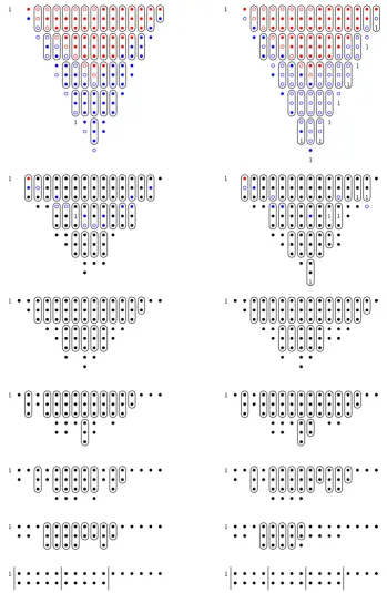
bits with a 1, which is a special case of a HA, rather than a FA. 10 2.5 Adder tree diagrams for the 4-bit CMAC for the real (left tree) and
imaginary (right tree) parts of the result of the cross-correlation operation. Red and blue colour denote partial product bits from
different multiplications. 11
2.6 Adder tree diagrams for the 8-bit CMAC for the real (left tree) and imaginary (right tree) parts of the result of the cross-correlation operation. Red and blue colour denote partial product bits from different multiplications. The vertical lines for the output of the tree denote the placements of 4-bit and 5-bit CLA sections. 12 2.7 Transistor-level schematic diagram of the FA circuit that has been
used throughout most of this work. The sum output is S and the
carry-out output is Co. 13
2.8 The conventional static FA circuit[32]. This is one of the structures that is used in the provided standard cell library. 14 2.9 A pass-transistor implementation of a FA. This is one of the
struc-tures that is used in the provided standard cell library. 14 2.10 The HA schematic diagrams of (a) the circuit that is used in the
List of figures
2.12 Schematic diagram of the LM DET flip-flop as used inside the CMACs’
accumulators. 16
2.13 Layout view of the LM DET flip-flop from Figure 2.12 as used inside
the CMACs’ accumulators. 16
2.14 The schematic diagram of the pulse generator circuit of the pulsed-latch flip-flop that is shared among several pulsed-latches. 17 2.15 Schematic diagram of the reset version of the pulsed latch. 17
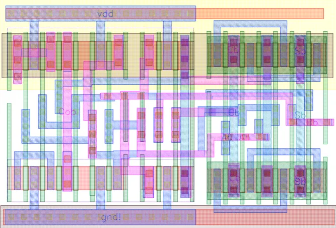
2.16 Layout of the 4-bit CMAC. 18
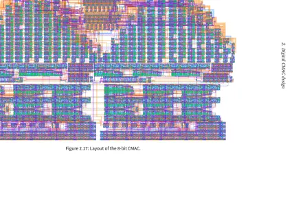
2.17 Layout of the 8-bit CMAC. 19
2.18 Layout for the imaginary part of the 4-bit CMAC. 20 2.19 Layout for the imaginary part of the 8-bit CMAC. 20
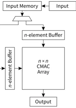
3.1 Simplified diagram of the internal structure of one processing unit
of Architecture 2 in[18]. 22
3.2 The example of how a correlation triangle is split into SIs for the case ofw=4. Numbers represent the four signal sets. (a) shows how a full integration is first split into sections. (b) shows the final pattern of SIs after auto-correlation sections are paired together
into full SIs. 22
3.3 Architecture of one multiple-accumulator CMAC witha accumulat-ors. The “Accumulator Select” circuit chooses which accumulators are read from and written into in the current processing cycle. 23 3.4 The illustration showing how (a) SIs for the case ofw=5 can be
grouped into (b) groups of 3 following the rules in Section 3.2. The arrow indicates the swapping of SIs that is performed before grouping. 24 3.5 Plot of the improvement ratioIover the one-accumulator array
againstwfor two cases ofa. 26
3.6 Comparison of the schematic diagrams of the two data storage circuits employed in the four CMAC designs: (a) standard Latch-MUX DET FF from Section 2.3.2 for one-accumulator designs and (b) custom 3-bit variant of the same circuit for three-accumulator designs. The 3-bit circuit is only twice the size of the 1-bit circuit. E1 through E4 are the locally-generated enable signals. 27
4.1 Transistor-level implementations of a C-element that are used in this work: (a) the weak-feedback and (b) the symmetric[45]
im-plementations. 31
4.2 Gate-level schematic of the new LG_C DET flip-flop using (a)
non-inverting and (b) non-inverting C-elements. 31
4.3 Operational waveforms showing the behaviour of the LG_C flip-flop. 32 4.4 Schematic diagram of a generic Latch-MUX flip-flop. 32 4.5 Operational waveforms for a generic Latch-MUX flip-flop. 32 4.6 Proposed transistor-level design of the LG_C flip-flop based on
weak-feedback C-elements shown in Figure 4.1a. 33
4.7 Transistor-level schematic diagram of the implicit-pulsed IP_C DET
flip-flop. 34
4.8 Gate-level schematic diagram of the implicit-pulsed IP_C DET flip-flop. 34 4.9 Logic waveforms showing the behaviour of the IP_C DET flip-flop. 35
flip-flop that uses 5 C-elements including weak devices for the inner
C-elements. 35
4.11 Gate-level schematic of the FN_C DET flip-flop shown in Figure 4.8 with 2 inner 3-input weak C-elements exhibiting a floating-node
behaviour. 36
4.12 Simulated signal levels of the implemented FN_C flip-flop. Floating
states are denoted as “~”. 36
4.13 Transistor-level schematic diagram of the conditional-toggle CT_C
DET flip-flop. 38
4.14 Simulated signal levels of the CT_C flip-flop implemented in the GF
28HPP technology. 38
4.15 Transistor-level schematic diagram of the improved
conditional-toggle CTF_C DET flip-flop. 38
4.17 Transistor-level schematic diagrams of the six previous DET flip-flop designs that are considered in this work for comparison with the new DET flip-flops. All circuits include input, output and clock buffering. The flip-flops are (a) LM[37], (b) EP[38], (c) LM_C
[46], (d) TSP[48], (e) CP[34]and (f) IP[43]. 41 4.18 Illustration of the procedure for measuring the worst-case minimum
D–Q delay. This plot is for a particular Monte Carlo point of the LM flip-flop. The curves are for the four cases of CK and Q transitions. The worst-case minimum D–Q delay is marked on the plot and also
on they-axis astdq. 43
4.19 Plot of the CK–Q delay versus the supply voltage for new flip-flops
and two previous LM and EP designs. 47
5.1 Architecture of the SAM memory. 50
5.2 Schematic diagrams of the sense amplifier: (a) the general diagram and (b) its transistor-level circuit.Vbis the voltage on the bitline andVpis the precharge voltage equal to 0.5VDD. 51 5.3 Top-level architecture of the fabricated chip. 52 5.4 The schematic diagram of the Clock Generator circuit. 52 5.5 The schematic diagram of the Charge Pump circuit. 53
5.6 The layout of the designed memory prototype. 54
5.7 The chip photo of the fabricated memory prototype. 55 5.8 Schematic of the test circuit with the fabricated chip. 55 5.9 Oscilloscope traces of (CH1, blue) the power supply voltage and
(CH2, red) the output voltage of the charge pump during operation
at high clock frequencies. 57
5.10 Oscilloscope traces of (CH1, blue) the VCO control voltage and (CH2, red) the output voltage of the charge pump when the VCO control voltage is varied manually. Note the different voltage scales
for the two traces. 57
5.11 Oscilloscope traces of (CH1, blue) the VCO control voltage and (CH2, red) the output voltage of the charge pump when the VCO control voltage is generated externally to be a low-frequency
List of figures
5.12 Voltage traces of (CH1, blue) the VCO control voltage and (CH2, red) the “E” signal which indicates correctness of operation as reported
by the built-in self-test circuits. 58
5.13 Correct traces of (CH1, blue) the “CK_out” and (CH2, red) the “mem_state” signals which are respectively one eighth and one
fourth of the internal clock frequency. 59
5.14 Voltage traces of (CH1) the “CK_out” and (CH2) the correctness “E” signals as reported by the chip at a low clock frequency. The
memory operates correctly. 60
5.15 Voltage traces of (CH1) the “CK_out” and (CH2) the correctness “E” signals at 773 MHz of internal VCO frequency. The “CK_out” trace does not appear to be square wave because of the 100 MHz
bandwidth limit of the oscilloscope. 60
5.16 Voltage traces of (CH1) the “CK_out” and (CH2) the correctness “E” signals when the VCO is at about 1.2 GHz. The memory works correctly. The “CK_out” trace does not appear to be a square wave because of the 100 MHz bandwidth limit of the oscilloscope. 61 5.17 Voltage traces of (CH1, blue) the “CK_out” and (CH2, red) the
correctness “E” signals as reported by the chip when the VCO is at above 1.2 GHz. This is the clock frequency for which the memory begins to fail. The “CK_out” trace does not appear to be a square wave because of the 100 MHz bandwidth limit of the oscilloscope. 61
6.1 Block-level diagram of the transmitter circuit. 62 6.2 The layout of the self-biased folded cascode differential amplifier. 63
6.3 Diagram of the LVDS clock receiver. 63
6.4 The layout of the designed clock reference input amplifier. 65 6.5 Schematic diagram of the implemented LC-tank oscillator. 66
6.6 The layout of the 3-to-1 serialiser. 67
6.7 The layout of the 11-to-1 serialiser. 68
6.8 The layout of the 66-to-1 serialiser. 69
6.9 The layout of the predriver circuit. 70
6.10 The schematic diagram of the designed SST driver. 71 6.11 The layout of the implemented SST driver. The image shows one
half of the pseudo-differential driver design. 72 6.12 The layout of the transmission gates that can be used to regulate
the driver’s impedance. 73
6.13 The layout of the bias generator circuit. 74
6.14 The layout view of the replica biasing transistors within the biasing
circuit. 75
3.1 Summary of the design information and simulation results of the 4-bit and 8-bit CMACs with one and three accumulators. 28
List of acronyms and abbreviations
AC Alternating current
ASIC Application-specific integrated circuit
CLA Carry-lookahead adder
CMAC Complex multiplier-accumulator
CML Current-mode logic
CMOS Complementary metal-oxide semiconductor
CSA Carry-save adder
CV Coefficient of variation
DAC Digital-to-analog converter
DC Direct current
DET Dual-edge-triggered
DFT Discrete Fourier Transform
DRAM Dynamic random-access memory
DTSCR Diode-triggered silicon controlled rectifier
EDA Electronic design automation
eDRAM Embedded dynamic random-access memory
ESD Electrostatic discharge
FA Full adder
FF Flip-flop
FFE Feed-forward equaliser
GF GlobalFoundries
HA Half adder
IC Integrated circuit
IDDQ Leakage current
I/O Input/output
IP Intellectual property
LVDS Low-voltage differential signalling
MC Monte Carlo
MOSFET Metal-oxide-semiconductor field-effect transistor
MSB Most significant bit
MUX Multiplexer
PDP Power-delay product
PFA Partial full adder
PLL Phase-locked loop
PRNG Pseudorandom number generator
PVT Process, voltage and temperature
RAM Random-access memory
RSD Relative standard deviation
SAM Sequential-access memory
SCR Silicon controlled rectifier
SD Standard deviation
SerDes Serialiser/deserialiser
SET Single-edge-triggered
SI Sub-integration
SST Source-series termination
VCO Voltage-controlled oscillator
Chapter 1
Introduction
This work deals primarily with the design of integrated circuits. The introductory chapter provides background information about radio astronomy, multi-element radio telescopes, radio interferometry and correlators. The chapter also presents motivations and the overview of this work.
1.1
Telescopes with multiple antennas
Radio astronomy is a field of science that deals with observations of space objects such as stars and galaxies in radio spectrum. There are different types of radio telescopes that can image these objects. Telescopes employ different imaging tech-niques depending on the number of antennas that they consist of: single-antenna telescopes measure the image directly and telescopes with multiple antennas calculate the image from the measured signals.
The two types of telescopes are related. For a single-dish telescope, the max-imum angular resolutionθis limited by the effects of diffraction and is given by the following relationship between the wavelength of the observed signalλand the diameter of the dishD[1, Ch. 6]:
θ = λ
D. (1.1)
Multi-element telescopes use signal processing techniques that allow multiple antennas to act as a single imaging instrument with the maximum resolution equivalent to that of a single-dish telescope the size of the entire antenna array[1, Ch. 9]. For example, antennas separated 10 000 km apart can produces images as large as a single dish that is 10 000 km in diameter. Thus, only a few antennas are enough to be able to generate a high-resolution image. Although increasing the number of antennas while keeping the same maximum separation does not increase the maximum resolution, using more antennas increases the total collecting area, which improves many other important characteristics of the telescope such as its sensitivity and the survey speed[2, Sec. 6.5].
The process of combining signals from multiple antennas to generate a single image is called aperture synthesis[1, Ch. 9],[2]. One of the key techniques of aperture synthesis is interferometry. The use of interferometry can be explained with the help of Figure 1.1 which shows a diagram of two antennas receiving signals from different sources. Although each antenna measures the sum of all signals, the distance that separates these antennas ensures that phase differences between these signals are different for different antennas. Interfering signals for every
Figure 1.1: Diagram of two antennas receiving two signals. Although both antennas receive the sum of the two signals, the phase difference between these signals is different for different antennas.
antenna pair allows the interferometer to extract this information and ultimately reconstruct the image. Modern telescopes use the cross-correlation operation for this purpose, which is implemented inside the correlator.
1.2
The correlator
The correlator produces a cross-correlation signal for every distinct pair of antenna signals. Every such pair is called a baseline. Every signal is also correlated with itself to produce an auto-correlation baseline. Since dual-polarisation antennas produce two signals, an array ofNsuch antennas produces 2Ninput signals for the correlator. This amounts to(2N2−N)cross-correlation baselines and 2N auto-correlation baselines making the size of the correlator scale at least quadratically withN.
The cross-correlation operation measures how similar the correlated signals are as a function of time displacement or lag. Time-domain correlation of signals s1ands2can be written as follows[3, p. 401]:
(s1?s2)[t] =
∞ X
a=−∞
s∗1[a]·s2[a+t], (1.2)
wheres∗1is the complex conjugate ofs1and the indices are time instances. In practice, sequence lengths and summation bounds are chosen to achieve a specific frequency resolution after the frequency transform. When correlating in frequency domain, the output for each frequency channel ccan be written as a complex multiplication[4, pp. 46 and 243],[5, p. 219]:
(s1?s2)[c] =s1∗[c]·s2[c]. (1.3)
Frequency channelisation itself is performed by the DFT; however, modern tele-scopes use more complicated frequency transformations[6].
cross-1. Introduction
correlates in time domain and the FX correlator that cross-correlates in frequency domain. The idea for the FX correlator was proposed in[8]. WhenNis large, the FX structure is computationally more efficient than the XF structure, which was explained in[9]and[10]for its first implementation. Whereas both X and F are proportional toN2in an XF correlator, only the X part is proportional toN2in an FX correlator while the F part is proportional to justN. This follows from the fact that the F part processes individual antenna signals in the FX correlator rather than the correlation signals for each baseline as in the XF correlator.
For each baseline, the correlator output consists of integrated data samples for allCfrequency channels. These data samples are called visibilities. Integration is performed by accumulating the correlated samplesT times for each frequency channel of each baseline.T is called the integration count and is related to the dump time of the correlatorτand the per-signal sample rateBwithT =τB.
The planned Square Kilometre Array radio telescope[11]will consist of sev-eral imaging instruments using multiple correlators with various parameters. For example, one of the modes of the SKA Mid correlator will process 8-bit data and will have the following parameters:C ≈250 000,N ≈254, B≈ 1.4 Gs/s and
τmin≈0.1 s. Other modes will use 8-bit, 4-bit and 3-bit data at different rates.
The first construction phase will see a smaller version of the SKA Mid built with N≈190 andC≈65 000[12].
This work focuses on the architecture and implementation issues of the X part of very large FX correlators when using very-large-scale integration (VLSI) technologies. These apply to correlators the size of the SKA and larger.
1.3
Motivation
Advances in computing technologies are essential to advances in science. Radio telescope interferometers are an example of this as their scientific capabilities are often limited by the processing ability of their supercomputers. The future telescope Square Kilometre Array is envisioned to be considerably larger in size and science output than any of the existing telescopes such as the ALMA[13], JVLA
[14], ASKAP[15], MWA[16]or LOFAR[17]. This scale is set to create challenges for the implementation of the telescope’s signal processing pipeline and especially its correlator.
A comparison can be made between the SKA and, for example, the LOFAR. The LOFAR consists of about 50 antenna stations, which makes it one of the largest telescopes currently in operation. The SKA Low instrument will be making observations in a similar frequency range but with about 1,000 antenna stations and with higher sensitivity and survey speed[11],[12]. The large number of stations alone will create more than a million baselines for the SKA Low’s correlator versus only a few thousand for the LOFAR. This increase is a significant challenge for the signal processing hardware as incremental improvements in computing technology will not allow existing solutions to be simply scaled up by orders of magnitude[18]. As the number of antennas increases, the correlator’s processing requirements experience quadratic growth and new methods and more efficient technologies are needed to be able to meet the technical requirements of such future telescopes. VLSI technologies deal with the creation of integrated circuits (ICs). Efficient implementation of custom signal processing circuits and tight integration between their various components can be achieved with application-specific ICs (ASICs).
on an ASIC. For example, custom circuits can be made to efficiently handle large-scale 4-bit arithmetic, which may not be possible without purpose-built hardware. Moreover, custom circuits can incorporate specific optimisations that improve their performance characteristics in a particular use case when compared against more universal designs.
High research and development costs of ASIC design are often a concern. With the SKA expected to be in operation for many decades, most of the SKA’s costs are likely to be incurred during the operation of telescope rather than its construction. The higher costs of ASIC development are thus likely to be offset by the ASICs’ reduced power dissipation and increased performance. The combination of efficiency and long-term value makes ASICs a good fit for long-term projects with demanding technical requirements, yet little effort has gone into IC design for modern correlators in modern CMOS technologies. This makes ASIC design of correlator circuits a relevant research topic.
1.4
Thesis outline
The thesis is organised into six chapters. Chapter 2 presents custom 4-bit and 8-bit CMACs that have been designed in a 28 nm CMOS technology. The presented designs are thoroughly optimised high-performance circuits suitable for use in an ASIC correlator. The designs merge the carry-save adder trees of the multipliers comprising each CMAC to minimise the use of expensive carry-lookahead adders. The circuits employ the dual-edge-triggered clocking scheme to reduce the clock power dissipation.
Chapter 3 considers the common input-buffered FX correlator construction and proposes incorporating multiple accumulators in every CMAC to reduce the utilisation of the input-buffer memory by a third. In this chapter the CMACs from Chapter 2 are adapted to include three accumulators per CMAC. The performance characteristics of such CMACs are evaluated and compared to conventional one-accumulator CMACs and are found to be at least as good. The three-one-accumulator 8-bit CMAC exhibits reduced power dissipation within its multiplier circuits due to reduced input switching activity, which more than makes up for the increased power dissipation within its accumulator circuits. This reduction in the CMAC power dissipation is in addition to the reduction in the memory.
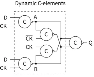
Chapter 4 continues on the topic of design of dual-edge-triggered storage elements that were used in the CMAC designs in Chapter 2 and adapted for the multiple-accumulator approach in Chapter 3. Five novel DET flip-flop designs are presented. The new designs are extensively evaluated in simulation and compared against a number of existing designs. The common features of these designs are the use of C-elements to reduce the energy dissipation due to glitches at the flip-flops’ data inputs.
1. Introduction
Chapter 6 presents the design of the full-rate 15 Gbps transmitter circuit in 28 nm CMOS. The design uses the 64b/66b line encoding scheme. The circuit includes the scrambler, the serialiser, the digital VCO with analog fine-tuning, the driver and the ancillary circuits. The driver is of the Source Series Terminated type. The driver consists of five segments for each of the four taps of the Feed Forward Equaliser and the amplitude-tuning segment. The replica biasing circuit takes as its input the FFE, impedance and amplitude parameters and sets bias voltages for all driving segments. The impedance is additionally controlled by adjusting the termination resistor to achieve better linearity. DTSCR-based ESD protection is employed with an asymmetric T-coil. The design of the LVDS 315.25 MHz reference clock input amplifier is also presented.
Finally, Chapter 7 concludes the thesis and gives an overview of potential future work. The appendix contains two sections: Appendix A details the netlists of the multiplier designs from Chapter 2 and Appendix B includes the list of publications that have been based on the work presented in this thesis.
Digital CMAC design
2.1
Complex multiplication and CMAC
Before the correlator circuits can be designed, their exact function needs to be ascertained. The key processing operation that the correlator performs is the complex multiplication as per the cross-correlation formula in (1.3). The complex multiplication of two numbersG=a+i bandH=c+idcan be written as follows:
G·H= (a+i b)(c+id) = (ac−bd) +i(ad+bc). (2.1) The complex conjugate is applied to one of the numbers before the multiplica-tion as per (1.3). This results in the following expression that the correlator circuits must implement:
G·H∗= (a+i b)(c−id) = (ac+bd) +i(bc−ad). (2.2) Although expressions (2.1) and (2.2) may look different at first glance, they are actually the same from the point of view of the implementation. This can be demonstrated by swapping the real and imaginary parts of one of the numbers before the multiplication:
(b+ia)(c+id) = (bc−ad) +i(ac+bd), (2.3)
which yields the same result as in (2.2) but with the swapped real and imaginary parts. Thus, the cross-correlation operation can be implemented with a regular complex multiplier with the outputs and some of its inputs relabelled as illustrated in Figure 2.1 in order to implement the complex conjugate.
The output from the complex multiplier is integrated using an accumulator. Strictly speaking, only the implementation of (2.1) along with an accumulator is a complex multiply-accumulator (CMAC). In this work the term CMAC is used to refer to the implementation of (2.2). This is justified because although (2.1) is mathematically different to (2.2), their implementations result in identical circuits only with different input and output port names.
2. Digital CMAC design
Re Im
Im Re Re(G)
Im(G)
Im(H) Re(H) Im(G)
Re(G)
Im(H) Re(H)
Figure 2.1: A complex multiplier can calculate the cross-correlation without per-forming the complex conjugate operation explicitly. This can be achieved by simply relabelling the ports for one input and relabelling the outputs as explained by (2.3). In this case, the real and imaginary parts of theGinput are swapped.
a c b d b c a d
Re Im
−
Re(A) Im(A)
Figure 2.2: CMAC functional diagram following (2.2) and including accumulators.
0 0 1 1 0 1 0 0 0 1 0 0 1 0 0 0 0 0 0 0 0 0 0 0
1 1 1
1 1 0 0 0 1 1 0 1 0 0 0 1
0 0 0 1
1 1 0 0 1 0 1 1 1 0 1 1
= 7272₁₀
Figure 2.3: Example of how a signed 4b×12b multiplication can be performed
without sign extensions. The two multiplication operands are−6, which is 1010 in
2’s complement binary, and−1212, which is 101101000100. The result is truncated
to 16 bits.
2.2
CMAC multiplier design
A multiplier generally operates on two input numbers, or operands, to produce the result of their multiplication at its output. Common parallel multipliers work by generating partial products which are then added up with an adder tree. Partial products themselves are 1-bit multiplications of each bit of the first operand by the entire second operand. The correlator implements signed arithmetic and thus the design of 2’s complement multipliers and adder trees is of interest. One of the features of naive 2’s complement additions is that all addition operands need to be extended to the bit-length of the final result, which in the case of a multiplier adder tree is a significant overhead. This can be avoided by using the method first introduced in[19]which is now called the Baugh and Wooley multiplication method.
Figure 2.3 shows an example of how an adder tree of a signed multiplication can be done without sign-extending the partial products. The sign extension for each partial product is dealt with by adding a 1 at its MSB position, which has the effect of inverting the MSB and zeroing out the sign extension. These 1s are subtracted from the result, which explains the two leftmost 1s in the diagram. Adding 1s at MSB positions and subtracting them from the final result effectively removes the sign extension for the second multiplication operand. In order to remove the sign extension for the first operand (i.e., in order to not produce more partial products than there are bits in the first operand), the last partial product is subtracted rather than added. As the diagram illustrates it, handling partial products this way works out to the correct result. Although this exact method is not the same as the Baugh and Wooley multiplication algorithm, methods that use extra 1s and subtract some partial products are generally credited to them.
After partial products are generated, they are added up with the help of an adder tree. Common parallel adder tree construction methods include the Wallace tree[20]and the Dadda tree[21], which are both carry-save adder (CSA) tree variants. CSA trees work by adding up more than two numbers down to just two which are then added with a normal adder. Carry-save addition is attractive for adder trees because it is one of the constant-time addition methods whose delay depends only on the number of the addition operands rather than their bit-length
2. Digital CMAC design
at the output of CSA trees to resolve the carry signals of the carry-save encoding instead of the more common but slower ripple-carry adders. The CLA structure was chosen not only because of its speed but also its versatility in designing adders of various bit-lengths using a common set of CLA circuits[23].
A CSA tree is constructed from full adders and half adders that reduce the tree in sequential stages. A full adder (FA) is a circuit that adds up three bits of the same weight and outputs their 2-bit sum in the form of the sum bit and the carry-out bit. A FA is also known as the 3:2 compressor since it reduces its 3 inputs to just 2 outputs. A half adder (HA) is similar to a FA but it only adds up 2 bits of the same weight to produce 2 bits at the output. HAs do not reduce the tree since they produce the same number of outputs as they have inputs. HAs can thus be thought to only redistribute signals between weights.
The Wallace and Dadda tree construction algorithms are the most famous methods of determining exact positions of FAs and HAs, yet numerous other methods exist. This work uses the method described in [24]and [25], which is essentially a variant of the Wallace tree method that strives to minimise the use of HAs in favour of using more FAs. This achieves an overall reduction in hardware without compromising on anything else except perhaps the regularity of the tree. The comparison of this method to the Wallace tree is shown in Figure 2.4 which contains dot diagrams of adder trees for the signed 8-bit multiplication. The notation that is used in this work is similar to notations from[26]and[27]: each dot represents a single bit; a hollow dot denotes an inversion on the given bit, which only happens for some bits in the first stage of the tree to avoid sign extensions; encirclements of three bits represent placements of FAs and that of two bits represent HAs. Each two- and three-bit encirclement creates a sum bit, or a single dot, at the same weight and a carry-out bit for the higher weight in the next tree stage.
Based on the theory introduced above, multiplier adder trees for the 4-bit and 8-bit CMACs have been constructed. As per (2.2), the CMAC produces two numbers that are the real and imaginary parts of the complex-valued result. Rather than con-structing separate trees for each of the CMAC’s four multiplications, which would produce a regular CMAC design with four multipliers, the two multiplications for each of the real and imaginary parts are combined together into a single adder tree. In this way, the two adder trees calculate the result of the complex multiplication directly without explicitly producing the results of any of the individual multiplica-tions. This is more efficient considering area, timing and energy performance since fewer carry-resolution circuits of CLA adders have to be employed. Thus, each CMAC consists of only two adder trees, one for each of the real and imaginary parts of the output.
Figures 2.5 and 2.6 show the designed adder tree diagrams of the 4-bit and 8-bit CMACs. The presented adder trees are human-readable illustrations. The netlists detailing the internal tree signals and FA and HA placements for both CMACs are given in Appendix A. The following sections present the implementation of these CMACs including the details of their digital circuits.
2.3
Design of digital circuit cells
All circuits have been designed using the high-performance GF 28HPP CMOS technology. The development has mostly followed the approach of building larger
2.
Digital
CMAC
design
1
1
1
1
1
1
1 1
1
1
1 1
1
1
1
Figure 2.4: An example of the adder tree design for the signed 8-bit multiplication using the Wallace tree (left and centre columns) and the tree method from [25] that is used in this work (right column). The Wallace tree uses 38 FAs and 15 HAs while the design method uses 39 FAs and 7 HAs. Symbol “ 1 ” indicates the addition of two
bits with a 1, which is a special case of a HA, rather than a FA.
2. Digital CMAC design
1 1
1 1
1
1
1
1 1
1
1 1
1
1 1
1 1
1
1
1
Re Im
Figure 2.5: Adder tree diagrams for the 4-bit CMAC for the real (left tree) and imagin-ary (right tree) parts of the result of the cross-correlation operation. Red and blue colour denote partial product bits from different multiplications.
circuits from smaller circuit cells. Although a collection of standard cells is provided with this technology by a third party organisation, these cells have not been used in final versions of any design.
2.3.1 Adder circuits
The key building blocks of the adders used in this work are FAs and HAs. Their efficient implementation is thus key to the overall efficiency of any design that uses them. This is especially true for the FA cell, which is the most important cell of the adder trees.
Partial products are generated right before the adder tree. Their individual bits are 1b×1b multiplications of each bit of one multiplication operand with each bit of the other operand. A 1-bit multiplication can be implemented as an AND gate. However, the static CMOS circuit design style does not have an AND gate, only NAND. Simply inverting the output of a NAND to make an AND incurs a significant power overhead as the number of partial product bits is proportional to the square of the operands’ bit-length. Although due to De Morgan’s laws, the AND gate can be implemented with a single NOR gate as follows:
A·B=A+B, (2.4)
the NOR gate is slightly less energy efficient than the NAND gate for the same timing performance, which is due to its use of larger p-type transistors. Thus, the simple NAND gate was chosen to generate “active low”, or inverted, partial products. Accordingly, all of the adder tree circuits have been designed to have
1 1
1
1
1
1
1
1
1
1
1 1
1 1
1 1
1 1
1
1
1
1
1
1
1 1
1 1
1
1
[image:25.595.123.473.118.654.2]Re Im
2. Digital CMAC design C C A C C A A A A A S C C C C B B
VDD VDD
VDD A B C B A A B C A B Co A A B B C C
Figure 2.7: Transistor-level schematic diagram of the FA circuit that has been used throughout most of this work. The sum output is S and the carry-out output is Co.
“active low” inputs and outputs. It can be noted that there is no difference between the “active low” and “active high” versions of the FA as simply inverting all values in its truth table[28, p. 119]yields the same table. The “active low” notation is still kept for the FA for the sake of consistency.
The schematic diagram of the FA that has been used throughout most of the multiplier circuits in this work is shown in Figure 2.7. The circuit uses the standard static carry generation circuit and a pass-transistor version of the 3-input XOR circuit shown in [29]. The XOR3 circuit construction is similar to CMOS pass-transistor and double pass-pass-transistor circuit construction style of[30]and[31]. The use of unbuffered outputs from pass-transistor circuits actually complicates adder tree construction, because such an output should not be used as the input into the pass-transistor circuit again. Compared to the conventional FA circuit[32] shown in Figure 2.8, for the same number of transistors this design is inherently slightly faster as its critical path has fewer inverters.
The provided standard cell library includes several FA implementations that use two circuit topologies shown in Figures 2.8 and 2.9. Compared to the provided cells, the designed FA has been found to reduce the power dissipation of the adder trees in which it is used by more than 30% for the same timing performance. This has been found to be mostly due to the different transistor sizing approaches. The provided cells use transistors that are much larger than the optimal size from the point of view of the energy-delay trade-off in order to reduce circuit area. Even though transistors in these cells are large, certain routing techniques become possible with large transistors that reduce the space between n-type and p-type transistors thus reducing the overall area.
The designed HA circuit is shown in Figure 2.10 along with the provided standard cells. The designed HA has a shorter critical path when compared to the provided circuit. Just as the designed FA circuit, the HA uses a pass-transistor XOR to generate the sum signal.
Another important adder circuit is the CLA, which is used at the output of every adder tree and also in places where just two numbers need to be added. The CLA is the parallel adder structure introduced in[33]to speed up the addition of two numbers. The implemented CLA circuits include the partial full-adder (PFA) and carry-lookahead circuits constructed from NAND gates. Both the standard and
VDD VDD VDD VDD VDD VDD A B C B A A B C A B
A B C
A B C
B A C C A B Co Co Co Co S
Figure 2.8: The conventional static FA circuit [32]. This is one of the structures that is used in the provided standard cell library.
A B A Bi A A Bi B B Co S C
Ai A A
Bi Ci C B C B C C
Figure 2.9: A pass-transistor implementation of a FA. This is one of the structures that is used in the provided standard cell library.
S B B A A A A A B Co A A B B VDD Co Co A A B B S A B Co Co (a) (b)
2. Digital CMAC design
Figure 2.11: The layout implementation of the FA circuit from Figure 2.7.
hierarchical CLA adder sections have been designed for the 4-bit and 5-bit CLAs. Although less common, 5-bit CLA sections give more freedom in the implementation of adders of various bit-lengths, for example, making it possible to implement a 20-bit adder as a two-level hierarchical CLA adder.
Transistors of the adder tree cells were sized to achieve the best power efficiency given the timing requirements. The cell layouts were created while following the technology manufacturability guidelines such as the recommended minimums for the sizes of various layout features, which is important for design robustness in advanced process nodes such as 28 nm. The example of a layout of an individual cell is shown in Figure 2.11 for the FA circuit of Figure 2.7.
2.3.2 Memory registers
Each CMAC is implemented as a two-stage pipeline. The first stage is the computa-tion of the cross-correlacomputa-tion and the second stage is the accumulacomputa-tion. Registers are used in between the pipeline stages and inside accumulator circuits. Registers have been implemented using dual-edge-triggered flip-flops (DET FFs).
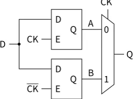
DET FFs achieve the same data rate as the more common single-edge-triggered (SET) FFs at half the clock frequency, which usually leads to reduced power dissipation of synchronous logic circuits[34],[35]. Although DET FFs are more complicated to handle in EDA tools than SET FFs, their use can easily be adapted to existing design flows[36]. CMAC circuits use a common design called the Latch-MUX (LM) DET FF[34],[37]which consists of two input latches multiplexed to one output. The LM FF is essentially a DET version of the common SET Master-Slave FF. A pulsed latch design similar to the ep-DSFF (EP) DET FF of[38]is also used on some critical paths to allow for dynamic time-borrowing as introduced in
[39]. Time-borrowing is also known as clock stretching.
The LM FF is the main flip-flop that is used throughout the design. The circuit diagram and layout for the variant that is used inside accumulators are shown in Figures 2.12 and 2.13. Multiple implementations of this FF have been made
CK CK
CK
CK CK
Q
CK
CK
CK CK R
R
Q D
Figure 2.12: Schematic diagram of the LM DET flip-flop as used inside the CMACs’ accumulators.
Figure 2.13: Layout view of the LM DET flip-flop from Figure 2.12 as used inside the CMACs’ accumulators.
to fit in various circuits. These implementations have different driving strengths, set/reset configurations and different data input and clock signal buffering.
The other FF type that is used in the CMACs is the pulsed latch FF. This FF is essentially a latch whose transparency is controlled by the pulse signal. This FF possesses the “soft-edge” property, which allows it to capture its data input up to a certain amount of time after the clock transition. This additional time is used to effectively extend the evaluation time of critical circuit paths beyond the duration of the clock cycle at the expense of the following pipeline stage. In the case of CMACs, this technique extends the evaluation time for the complex multiplication at the expense of the accumulation, which increases the maximum pipeline frequency without having to increase the number of pipeline stages.
2. Digital CMAC design
CK
CK
CK P
[image:30.595.209.388.71.141.2]P
Figure 2.14: The schematic diagram of the pulse generator circuit of the pulsed-latch flip-flop that is shared among several latches.
VDD VDD
P
P P
P D
R D
R VDD R
Q
Q
Figure 2.15: Schematic diagram of the reset version of the pulsed latch.
storage elements for the CMACs has spawned an effort to create more advanced DET flip-flops that are presented in Chapter 4.
2.4
CMAC implementation
Two CMACs have been created for the 4-bit and 8-bit input data. For the 4-bit design, the input data sample format is complex 8 bits (4 bits for each of the real and imaginary parts) and the output accumulation is complex 40 bits (20 bits for each part of the complex number) as is used in[40]. In the 8-bit design, the input is complex 16 bits and the output is complex 64 bits as is used in the SKA. The netlists for the adder tree circuits that detail internal tree signals and the placements of FAs and HAs inside the tree are given in Appendix A.
Figures 2.16 and 2.17 show the layouts of the implemented CMAC circuits for the 4-bit and 8-bit CMACs respectively. The circuit area for both designs is 1421µm2 and 3950µm2respectively. Figures 2.18 and 2.19 show adder tree
implementations for just the imaginary part of the cross-correlation operation of the two CMACs. In both cases the adder trees were designed in the shape of a triangle, which decreases local interconnect lengths despite potentially increasing the overall circuit area.
Post-layout analog simulations were performed to measure the performance parameters of the presented designs. Simulation parameters were chosen to simu-late realistic worst-case performance. The simulation temperature was set to 60 °C. The input data was generated randomly to have 35% switching activity on every bit. In terms of timing performance, the two designs could safely operate at 2 GHz and 1.25 GHz for the 4-bit and 8-bit CMACs respectively. At 2 GHz, the 4-bit CMAC was found to dissipate 1.94 mW. At 1.25 GHz, the 8-bit CMAC dissipates 3.27 mW.
[image:30.595.203.391.198.337.2]2.
Digital
CMAC
[image:32.595.154.710.115.450.2]design
Figure 2.17: Layout of the 8-bit CMAC.
Figure 2.18: Layout for the imaginary part of the 4-bit CMAC.
[image:33.595.129.468.456.713.2]Chapter 3
Multiple-accumulator CMACs for the
input-buffered FX correlator
CMACs are used to implement the X part of an FX correlator. A popular archi-tecture uses the input-buffered approach that reorders data from the F part for the convenience of processing in the X part. The F part naturally produces the entire spectrum of frequency channels for the time window on which it performs channelisation, yet a normal CMAC with a single accumulator can only integrate cross-correlations across time for the same frequency channel. This may create a need for an input buffer that can hold data samples for the entire period of the integration time and for all signals and the entire spectrum. This input buffer is also called a corner turner. The design of the corner turner itself is outside the scope of this work mostly because there is little that an ASIC implementation can bring to it since it only reorders data without performing any processing on it.
This chapter presents a new approach of using multiple-accumulator CMACs to reduce the utilisation of the input-buffer memory that is internal to the processing unit that contains such CMACs. In this chapterbxcanddxedenote the floor and ceiling operations respectively.
The chapter consists of five sections. Section 3.1 introduces the details of the considered architecture. Section 3.2 introduces the rules of grouping sub-integrations for multiple accumulators and explains the rationale behind reduced memory access. Section 3.3 quantifies memory access improvements. Section 3.4 presents and compares the designs of multiple-accumulator CMACs against the single-accumulator CMACs from Chapter 2. Section 3.5 concludes this chapter.
3.1
Architecture overview
The architecture for the X part of an FX correlator that is considered in this work was introduced in [18]as Architecture 2 and is further detailed in [40]. The architecture is intended for an ASIC implementation. The internal structure of one processing unit is shown in Figure 3.1. The main components are the input memory, the CMAC array and the two processing buffers. The input memory holds 2N T data samples for all 2N input signals, for one frequency channel and for allT time instances that occur over the period of the integration time. The key parameters of this architecture arenandw. Everyninput signals are grouped into
The content of this chapter appeared in a published article. Adapted by permission from Springer Nature: Springer Experimental Astronomy, “Using multiple-accumulator CMACs to improve efficiency of the X part of an input-buffered FX correlator”, S. Lapshev and S. M. R. Hasan, doi: 10.1007/ s10686-017-9527-4, ©2017.
n × n CMAC Array n-element Buffer n -element Buff er Output
Figure 3.1: Simplified diagram of the internal structure of one processing unit of Architecture 2 in [18].
« 1 2 « 11 « 1 3 « 2 3 « 33 « 22 « 1 4 « 2 4 « 44 « 3 4 « 1 2 1 3«
[image:35.595.235.361.71.251.2]« 2 3 « 1 4 « 2 4 « 3 4 « 11 « 22 « 33 « 44 (a) (b)
Figure 3.2: The example of how a correlation triangle is split into SIs for the case ofw= 4. Numbers represent the four signal sets. (a) shows how a full integration is first split into sections. (b) shows the final pattern of SIs after auto-correlation sections are paired together into full SIs.
a signal set, which amounts tow=d2N/nesignal sets. Everyndata samples read from or written to the memory for one signal set are referred to as a sample set in this work. Each of the two processing buffers (n-element buffers) holds one sample set. Each signal set is correlated with all wsignal sets by using then×narray of CMACs which can performn2cross-correlations in parallel. The CMAC array integrates correlations forT processing cycles. Every integration performed by the CMAC array is called a sub-integration (SI). An example of how a full integration for all signals can be split into SIs is shown in Figure 3.2. Auto-correlation half-SIs are paired together because the CMAC array can be processing two such half-SIs at the same time. In this architecture all SIs are processed in the same chip and by the same CMAC array.
3. Multiple-accumulator CMACs for the input-buffered FX correlator
Complex Multiplier Input A Input B
Accumulator 1
Accumulator 2
Accumulator a
...
Adder
Accumulator Select
[image:36.595.226.370.72.271.2]... ...
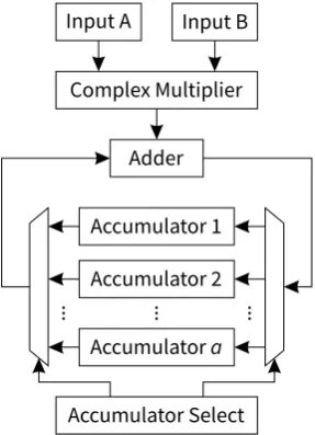
Figure 3.3: Architecture of one multiple-accumulator CMAC withaaccumulators. The “Accumulator Select” circuit chooses which accumulators are read from and written into in the current processing cycle.
The following sections detail how multiple accumulators per CMAC can be used to further reduce the number of memory operations and achieve larger power savings.
3.2
Grouping SIs for multiple-accumulator CMACs
During integration of a particular SI, in every processing cycle a one-accumulator array reads two sample sets which belong to the same time instance. For every new processing cycle, two new sample sets are read from the memory for the same two signal sets but for a different time instance. The array cannot switch to processing a different SI until it finishes the current SI and it thus has to read the same data samples again for all other SIs that correlate the same two signal sets with all other signal sets. The multiple-accumulator array can keep intermediate accumulations for multiple SI and can thus switch between different SIs in every processing cycle. The architecture of one multiple-accumulator CMAC withaaccumulators is shown in Figure 3.3. Regardless of the number of accumulators per CMAC, the CMAC array can only process one SI in each cycle. The reduction in the number of memory read operations is achieved when the same data samples that have been read for the current SI in one cycle are reused for a different SI in the next cycle. Grouping SIs enables fewer memory operations per processing operation without increasing or decreasing the number of processing cycles that need to be performed.
Withaaccumulators per CMAC, SIs need to be grouped into groups ofa. Each group of SIs is a sequence of several SIs. Each SI in the sequence has to share at least one signal set with the following SI in the sequence. In this way, for every time instant of the input data samples, the multiple-accumulator array reads two sample sets for the first SI in the sequence and then sequentially processes all the other SIs in the group while updating at most one sample set in the processing buffers in every cycle.
«
1 2 1 3« 1 4« « 2 4 « 1 5 « 2 5 « 3 5 « 4 5 « 55 « 11 « 22 « 33 « 44 «
1 2 1 3« « 3 4 « 1 4 « 2 4 « 2 3 « 1 5 « 2 5 « 3 5 « 4 5 « 55 « 11 « 22 « 33 « 44 « 2 3 « 3 4 (a) (b)
Figure 3.4: The illustration showing how (a) SIs for the case ofw= 5 can be grouped into (b) groups of 3 following the rules in Section 3.2. The arrow indicates the swapping of SIs that is performed before grouping.
For every SI that is composed of two auto-correlation half-SIs there is the cross-correlation SI that processes the exact same signal sets. Every paired auto-correlation SI and its cross-auto-correlation counterpart should be in the same group and should be processed in sequence. Then, no memory read operations are required for the processing of one such SI because the same sample sets would have already been read for the previous SI in the processing sequence. This is in contrast to the one-accumulator array where every processing cycle requires the update of the two sample sets in the processing buffers. Depending on the implementation, this has the potential advantage of making it easier to update the memory with new data samples for the next full integration.
Figure 3.4a shows a pattern of SIs and Figure 3.4b shows the example of grouping these into groups of 3. Essentially, all SIs are aligned in one sequence that is split into a new SI group after everyaSIs. The sequence starts from the bottom left of the correlation triangle and continues row by row left-to-right for the odd rows and right-to-left for the even rows. In this sequence every paired auto-correlation SI is always followed by its cross-correlation counterpart, but depending onwandathe cross-correlation SI may need to be swapped with the SI preceding the paired auto-correlation SI for the two SI to be in the same group. After such swapping, every SI still shares at least one signal set with the following SI in the sequence. The swapping is done once in this example as is indicated in Figure 3.4a. The same grouping strategy applies to any valid combination ofw anda. Numerous other ways of grouping SIs are possible and the most convenient way depends on the implementation.
3. Multiple-accumulator CMACs for the input-buffered FX correlator
3.3
Quantifying memory access improvements
The CMAC array has two data inputs for the two sample sets that it correlates in each cycle. In the case of the memory operating on one sample set per operation, every change of the array’s inputs corresponds to one memory read operation. As per the grouping approach presented in the previous section, the average number of times the array’s inputs change per 2Ninput data samples can be expressed as
R(a,w) = (a+1)A+ (B+1)sgnB−jw
2
k
sgn(a−1)
+ (wmod 2) (1−sgnB), (3.1)
where
A=
w2/2 a (3.2) and B= w2 2
moda. (3.3)
In (3.1)–(3.3), ais the number of accumulators per CMAC and wis the total number of signal sets as per the definitions in previous sections;Ais the number of full SI groups each withaSIs andBis the number of remaining SIs that form an incomplete group. In these relationshipsbw2/2cis the total number of full SIs including the paired auto-correlation half-SIs. The number of these half-SIs isw which are paired to formbw/2cfull SIs. There is an unpaired half-SI whenwis odd.
The expression definingR(a,w)in (3.1) is composed of several terms. The first term is the number of memory read operations normally needed for full groups: There areAsuch groups each normally contributing(a+1)memory reads. The second term is the number of memory reads for the remainingB full SIs which normally account for(B+1)memory read operations. WhenBis 0, the second term is also 0 rather than(B+1). The third term takes into account the paired auto-correlation SIs and subtracts their number from the first and second terms. For this to be correct, the groups that include auto-correlation SIs also have to include the cross-correlation SIs that process the exact same signal sets, which reduces the number of required memory reads from(a+1)and(B+1)by 1 for every pair of auto-correlation and the corresponding cross-correlation SIs in the same group. The third term is 0 whenais 1, because in this case it is not possible to have the auto-correlation and the corresponding cross-correlation SIs in the same group. The fourth term takes into account the remaining unpaired auto-correlation half-SI by adding an additional memory operation only whenwis odd andBis 0: Whenwis even, there is no unpaired half-SI; whenwis odd andBis non-zero, the unpaired half-SI is included with the incomplete group that also includes theBfull SIs. In the latter case, the signal set processed by the unpaired half-SI must be one of the signal sets processed by at least one of theBfull SIs so that its processing does not require an additional memory operation.
The total number of data samples read from and written to the memory per one full integration (i.e., per 2N T data samples) is thus
M(n,T,w,a) =nT(R(a,w) +w). (3.4)
Impr
ovement r
atio
I
(
a
,
w
Number of signal sets w 0.5
0.6 0.7 0.8 0.9 1
1 3 5 7 9 11 13 15
a 3
a 8
Figure 3.5: Plot of the improvement ratioIover the one-accumulator array against wfor two cases ofa.
Equation (3.4) generalises the required memory access per one full integration using the multiple-accumulator CMAC array. The value ofM(n,T,w, 2)represents both values derived in[41]for the two-accumulator array. The improvement ratio over the one-accumulator CMAC array can be expressed as
I(a,w) = M(n,T,w,a) M(n,T,w, 1)=
R(a,w) +w
w2+w . (3.5)
The larger w is, the less I(a,w)depends on w. For w larger than a, I can be approximated with
I' a+1
2a . (3.6)
The improvement ratio represents the reduction in the number of input memory operations. Consequently, it also represents the reduction in the memory’s dynamic power dissipation. The inverse ofImay also represent the increase in performance for memory-limited implementations. Figure 3.5 shows the value of the improve-ment ratioIagainstwfor two cases ofa: the reduction in the number of memory operations is more than 30% and 40% whenais 3 and 8 respectively.
3. Multiple-accumulator CMACs for the input-buffered FX correlator E D Q D CK CK Q E D Q
CK CK CK
E D Q D E2 Q E D Q E4 E D Q E4 E D Q E1 E3
E4 E1 E1 E2 E2 E3 E3
[image:40.595.159.439.70.279.2](a) (b)
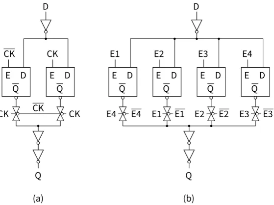
Figure 3.6: Comparison of the schematic diagrams of the two data storage circuits employed in the four CMAC designs: (a) standard Latch-MUX DET FF from Section 2.3.2 for one-accumulator designs and (b) custom 3-bit variant of the same circuit for three-accumulator designs. The 3-bit circuit is only twice the size of the 1-bit circuit. E1 through E4 are the locally-generated enable signals.
M(mn,T,d2N/(mn)e, 2). Depending on specific numbers, this would result in at least a further 25% reduction for a large number of such SI super-groups.
3.4
Design and evaluation of multiple-accumulator CMACs
It was estimated for a proposed ASIC implementation of a one-accumulator archi-tecture in[40]that the input memory is responsible for about 20% of the total chip power with most of the rest (about 51%) being dissipated in the CMAC array. It is thus important to consider the impact of the multiple-accumulator approach on the CMAC array.
In addition to the two one-accumulator CMACs from Chapter 2, two more designs have been made to evaluate the multiple-accumulator approach in terms of its benefits and costs to performance parameters such as the energy dissipation, leakage, circuit area and circuit delay.
A naive design approach to multiple accumulators would be to simply use as many FFs as there are bits that need to be stored. Better designs are possible because the multiple values stored in the accumulator are never accessed at the same time. In general, the exact choice of design depends on the value ofaand the implementation technology. Figure 3.6 shows the schematic diagrams of the static data storage circuits that are used in the CMACs designed for this evaluation. The one-accumulator storage uses a standard DET FF design (Figure 3.6a) as was explained in Section 2.3.2. The three-accumulator designs use the storage element shown in Figure 3.6b that is a variation of the DET FF circuit with the same Latch-MUX construction. These storage circuits use inverters, transmission gates and D latches. Compared to the standard FF that uses two D latches per 1 bit of storage, the multiple-accumulator storage element uses(a+1)D latches to store abits. Instead of using the clock signal directly, this storage element uses(a+1)
and 8-bit CMACs with one and three accumulators.
Parameter or Metric 4-bit CMACs 8-bit CMACs
Temperature, °C 60
Cycle time, ns 0.5 0.8
Accumulator count 1 3 1 3
Etotal, pJ 0.972 1.031 2.614 2.578
ECMUL, pJ 0.400 0.347 1.619 1.373
EACC, pJ 0.572 0.684 0.995 1.205
IDDQ_total, µA 88.8 96.5 228.8 243.1
IDDQ_ACC, µA 43.5 51.2 60.3 74.6
locally-generated enable signals which sequentially switch in every clock cycle and only one of which is active at the same time. In this case the three-accumulator storage circuit is only twice the size of the standard one-accumulator FF which is a significant improvement over naive scaling.
Only the data storage circuits in the accumulators are different between the one- and three-accumulator CMACs of the same data wordlength. A specific imple-mentation of the circuits shown in Figure 3.6 presents many trade-offs including the ones between energy and delay as is investigated for similar circuits in Chapter 4. In this case these circuits have been designed so that the timing performance of one- and three-accumulator CMACs is equivalent.
Per-cycle energy dissipation of the CMAC circuits was measured precisely using post-layout analog simulations on netlists that include the extracted RC parasitics. The simulated energies include the energy costs of local clock distribution. Input data pattern was generated pseudo-randomly with each bit having a 35% prob-ability of switching in every cycle. Simulations were carried out for the typical process corner with the temperature set to 60 °C. Leakage currents were simulated using the dedicated IDDQ models provided with the technology design kit. Table 1 summarizes the relevant design information and simulation results of the four CMAC designs. In the tableEtotalis the total average per-cycle energy dissipation of a CMAC circuit;ECMULis part ofEtotalthat is dissipated in the multiplier part of the CMAC;EACCis the difference betweenEtotalandECMULthat represents the per-cycle energy dissipation of the accumulator part of the CMAC including the adder performing accumulations;IDDQ_totalis the total leakage current of the CMAC andIDDQ_ACC is that of the accumulator part of the circuit including the adder.
Because the high-speed adders dominate the circuit area of the CMACs’ ac-cumulator parts, the impact of using three acac-cumulators compared to just one is small in the metrics of area and leakage. The increase in the leakage is about 8.7% and 6.3% overall and about 18% and 24% for only the accumulator parts in the 4-bit and 8-bit cases respectively. The increase in circuit area is about 5.3% for the 8-bit case. For the 4-bit case, the designed one-accumulator layout is not as area-optimized as the other layouts and only a 5.5% reduction in area was achieved when compared to the three-accumulator design.
3. Multiple-accumulator CMACs for the input-buffered FX correlator
between clock cycles. The increase in EACChas been found to be mostly due to increased switching activity in the adder and to a lesser extent due to a more complex data storage circuit. The increase in the adder is due to processing of accumulations for different baselines in different clock cycles.
The reduction inECMULhas been found to outweigh the increase inEACCfor the 8-bit CMACs. For the 4-bit CMACs the net effect has been found to be an increase in the overall energy dissipation. Etotal is decreased by 1.4% for the 8-bit case and is increased by 6.1% for the 4-bit case. Larger overall power savings can be expected for larger wordlengths as the multiplier becomes more significant than the accumulator part.
Considering only multipliers, the reduction in the switching activity results in the decrease ofECMULby 13% and 15% in the 4-bit and 8-bit cases respectively. For the processing cycles when one of the data inputs stays unchanged between clock cycles, the decrease is about 20% and 25% for the 4-bit and 8-bit CMACs respectively. This presents an incentive of using a larger number of accumulators per CMAC to increase the number of such cycles and decrease the average power dissipation.
Increasingaresults in diminishing returns for the input memory savings as per (3.5) and (3.6). If only memory savings are considered, there may be little point in values ofagreater than 4. On the other hand, using largerais shown to decrease the power dissipation of the CMAC array which could be dominating the overall power dissipation as discussed in the beginning of this section.
3.5
Conclusion
The approach of grouping sub-integrations for efficient processing by the multiple-accumulator CMAC array has been presented. With such CMACs being able to switch in every cycle between different SIs sharing some data inputs, significant reduction in the number of memory read operations is achieved for the same number of processing operations and the same number of CMACs. With only three accumulators per CMAC, the total number of memory operations and thus the memory power is reduced by more than a third for an arbitrarily large number of input signals when compared to a one-accumulator CMAC array.
In addition to the two CMACs presented in Chapter 2, two more CMACs with multiple accumulators have been designed and evaluated. The multiple-accumulator approach has been found to result in the 1.4% decrease in the overall CMAC power dissipation in the case of three-accumulator 8-bit CMACs, which is in addition to a more than 30% reduction in the memory. Larger power savings can be expected for larger input data wordlengths and a larger number of accumulators.