Rochester Institute of Technology
RIT Scholar Works
Theses
Thesis/Dissertation Collections
1997
Design and process development of an integrated
phosphor field emission device
Robert Langley
Follow this and additional works at:
http://scholarworks.rit.edu/theses
This Thesis is brought to you for free and open access by the Thesis/Dissertation Collections at RIT Scholar Works. It has been accepted for inclusion
in Theses by an authorized administrator of RIT Scholar Works. For more information, please contact
Recommended Citation
Design and Process
Development of an Integrated
Phosphor Field Emission Device
by
Robert
1.
Langley
A Thesis Submitted
In
Partial Fulfillment
of the
Requirements for the Degree of
MASTER OF SCIENCE
In
Microelectronic Manufacturing Engineering
Approved by:
Professor
Michael R. Potter
(Thesis Advisor)
Professor
Santish K. Kuninee
Professor
Lynn
F.
Fuller
(Department Head of
J.1E)
DEPARTMENT OF :MICROELECTRONIC ENGINEERING
COLLEGE OF ENGINEERING
Design and Process
Development of an Integrated
Phosphor Field Emission Device
by
Robert
J.
Langley
I, Robert 1. Langley, hereby grant permission to the Wallace Memorial
Library of the Rochester Institute of Technology to reproduce this document
in
whole or in part that any reproduction will not be for commercial use or
profit.
Acknowledgements
I
amvery
thankful
for
the
support
ofmy
thesis
committee, Mike
Potter,
Dr.
Santosh
Kurinec,
and
Dr.
Lynn Fuller
for
their
guidance
withthis
project.
I
amalso
thankful
to
Advanced Vision
Technology
for providing financial
andtechnical
supportfor
this
study.Diane Potter
is
much
to thank
for
the
many
pictures
of equipmentand
working
devices.
In addition, I
wouldlike
to
thank
Scott
Blondel,
Dave
YackofF,
andClay
Reynolds,
for
Abstract
An Integrated Phosphor Field
Emission
Device
(IPFED)
has been fabricated
atthe
Rochester Institute
ofTechnology
for
the
purposeof
developing
a
new,
flat
paneldisplay
technology.
The
device
incorporates
anew,
cathodoluminescent,
thin
film
phosphor(Ta2Zn308)
developed
at
RIT
as
an anode.A
cathodeand
controlgate,
both
consisting
of a
thin
layer
of molybdenumare also
included in
the
device.
Electrons
are
tunneled
from
the
cathode viaFowler-Nordheim
tunneling
to
energetically
strikethe
phosphoranode.
The
anodethen
produceslight,
viacathodoluminescence,
whichthe
human
eyecan
detect.
Standard
semiconductor processes were utilizedin
the
fabrication
ofthe
device.
These
processes
include;
sputtering
ofZinc
Oxide,
tantalum,
molybdenum,
andquartz,
deposition
ofchemically
vapordeposited
(CVD)
oxide,
reactiveion
etching
oftantalum,
molybdenum,
and silicondioxide
using
CHF3/He,
CF4/H2,
orSF6
plasmas,
using
aG-line
stepper anddiazonaphthoquinone
(DNQ)
novolac resin resiststo
patternthe
aforementionedmaterials,
andutilizing
aRapid Thermal Processor
(RTP).
The
device
canbe
scaledfrom
ultrahigh
resolution(10
jim pitch orless)
to
standardSVGA
resolution
(0.28mm
pitch).Bright
(no
way
to
quantify)
pixels
have been
observed
at200nA
of currentat
100V
of
accelerationenergy.
The
control gate which wasbuilt into
the
structuredoes
not
function
asdesigned
due
to
shorting
problemsbetween
the
controlgate
and cathode.A
processfor
the
vacuum encapsulation ofthe
devices has
also
been
developed.
This
processdoes
notrequire
any
specialalignment
ofa separate
faceplate.
Many
ofthe
known
problems with otherfield
emissive
displays have
been
circumvented
Table Of Contents
Chapter
Page
1
.Introduction
12
2. Principles Of FED Operation
14
2.1 Types
OfFEDs
15
2.2 Fowler-Nordheim
Tunneling
20
2.3 Failure In
FEDs
24
3.
IPFED
Devices
Vs.
Other Types Of FEDs
25
3
.1
Anode
To
Cathode
Distance
26
3.2 Vacuum Encapsulation
OfFEDs
26
3.3
FED Phosphors
27
4.
Previous
Work
Related To The
Fabrication
Of IPFEDs
29
4. 1
Spindt
Type
Displays
29
4.2 Diamond-Like Carbon
Cathodes
31
4.3
Other
Reported Research
On
Lateral
Emitters
33
4.4
Reported IPFED Research
35
5. Design
Of Process
Flow
For The IPFED Device
37
5.1
Drawing
From The
Turkman/Pettinato Process
37
5.2
Design
Of IPFED
Mask
Set
39
5.3
The Use Of
Tantalum Zinc
Oxide In The IPFED
41
5.4 Initial IPFED
Process Flow
43
5.5
Etching
In
The
Plasmatherm
RIE
45
5.7 Lack
Of
A
Suitable
Mask For
The
Trench
Etch Process
51
5.8
UV Bake
Crosslinking
52
5.9
Formaldehyde
Crosslinking
53
5.10 Tri-Layer
Masking
Process
54
5.11
ASPR528
Thick Photoresist
55
5.12 SF6
Etch
Disruption
By
Chlorine
Chemistry
55
5.13 Development Of An SF6 Etch In The
GEC
Plasma Cell
56
5.
14
Visual Endpoint Detection In The
GEC
Plasma
Cell
60
5.15
SF6-CF4/H2 Polymer Problems
60
5.16
Cleaning
Of The
GEC
Cell Chamber Prior
To
CF4/H2
Etching
61
5.17 Endpoint Detection
By
Spectrometer
62
5.18
First Devices To
Be
Successfully
Fabricated
63
5.19 The Switch
To
Mo
Cathodes
64
5.20
Switch
From
Alternating
To Two
Step
Trench Etch
65
5.21 Description
Of
The Vacuum
Probe Station
66
5.22 Fabrication And
Testing
Of
Bare Si
Anode Short
Loop
67
5.23
The Need For An Etch
Stop
Layer
68
5.24 Fabrication
OfFirst Light
Emitting
IPFEDs
At
RIT
71
5.25
Loss Of Ta
Etch
Stop
Adhesion
To ZnO
72
5.26
Analysis Of
Functioning
IPFEDs
74
5.27
Use OfPolymeric
Residue
Removing
Chemicals
75
5.28 BOE/RTP
Processing
Experiments
77
5.30
Simulation
Of
Post
Trench Conditions On
Tantalum
Zinc Oxide
82
5.31
Testing
Strategies For IPFEDs
84
5.32
Finding
a
And
p
From
The I-V Data
Collected
86
5.33
Testing
For
Gate Control
87
5.34 IPFED
Failure
Analysis
89
5.35 Vacuum Encapsulation
91
5.35.
1
Resist Reflow Experiment
92
5.35.2
Si02
Sputtering
On
Top
Of Resist
94
5.35.3
Etching
Vias
Through
Si02
96
5.35.4 Removal
Of Resist
Under
Si02/Vacuum
Sealing
96
Table
ofFigures
Figure
Page
1
.Spindt, Lateral,
And
IPFED
FEDs
16
2.
Potential Well
Diagrams
20
3.
Fowler-Nordheim
Tunneling
Equations
22
4.
Melted Spindt
Emitter
24
5.
Metal And Si Spindt
Fabrication
Process
30
6.
Process
Flow For Lateral
Emitters
From Kim
etAl
33
7.
Dr.
Leonid Karpov's
Conceptual
IPFED,
Texas A&M
IPFED,
Device
Turkman/Pettinato
IPFED
36
8.
Pioneering
Process
Flow For 1st IPFED Device
44
9.
CF4/H2
Carbon To Fluorine Ratio
Graph
48
10.
SEMs Of Devices Etched
With
Too
Much
Carbon
In
Plasma
50
1 1
.GEC Plasma
Cell
Uniformity
Experiment Results
58
12.
1st SEM Of
Good
Emitter
64
13.
Fowler-Nordheim Plot From First Mo Emitter
67
14.
Cross Section Of
IPFED With
Blanket
Underlying
Ta,
IPFED With Patterned Ta
Etch
Stop
69
15.
SEMs Of
Buffered
Oxide
Etch
Experiment
73
16.
Picture
Showing
Ta Etch
Stop
Protecting
Underlying
ZnO
76
17.
SEMs
ofBOE/RTP
Experiments
78
18.
Thin ZnO
Etch
Stop
Experiment
81
19.
Tantalum Zinc
Oxide
Morphology
SEMs
83
20.
Fowler-Nordheim Data
(3
Curves/Plot)
85
21.
SEMs
Of Failed IPFEDs
90
22.
Schematic Of
Encapsulation
Process
93
23.
SEMs Of Wet Etched
Encapsulation
Vias
95
24.
SEMs
ofDry
Etched Vias
97
Tables
Table Number
Page
1
.Conditions
For
Cross-Linking
Experiment
19
2.
Conditions And Results From Formaldehyde Experiments
53
Table
ofAppendices
Appendix
A.
Turkman/Pettinato Process
Flow
B. Mask Layers
For
a
Triode IPFED Device
C.
Mask Layers For 10x10
Array
IPFED
Device
D. Information
On Operation And Calibration Of GEC Cell Mass
Flow Controller
E.
Uniformity
Experiment Results
F.
Vacuum
Probe Station
G.
Early
IPFED
Process Flow
(Flow
A)
H.
Photographs
Of
Working
IPFED Devices
I.
Photographs
Of
the
Cathodoluminescence
ofTantalum Zinc
Oxide Samples
J.
Mathcad Worksheet For
Calculating
a
And
P
K. Encapsulation
Masks And Process
Flow
L.
SEMs Of
Photoresist
After
Reflow
Experiments
M.
Modeling
Results
Using
Ansoft Software
Table
ofSymbols
AMLCD
Active
Matrix
Liquid
Crystal
Display
BOE
Buffered
Oxide
Etch
CRT
Cathode
Ray
Tube
EL
ElectroLuminescence
IPFED
Integrated Phosphor Field Emission Device
LPCVD
Low
Pressure Chemical Vapor Deposition
LTO
Low
Temperature Oxide
MT
millitorrRLE
Reactive Ion Etch
TZO
Tantalum
Zinc
Oxide
(Ta2Zn30g)
UV
Ultraviolet
Chapter
1
Introduction
Humans
are capable
ofperceiving
vastamounts
ofinformation
through
the
sense of sight.Because
of
this,
visualdisplays
are,
and
willcontinue
to
be,
the
primary interface between
people
andmachines1
Visual
displays
arecurrently
utilizedin
a plethora ofdevices
including
televisions,
desktop
and
laptop
computers,
automotive and aviationdisplays,
military
displays,
and virtualreality
goggles.Current
displays
aredominated
by
two
key
technologies,
the
cathode
ray
tube
(CRT)
and
the
active
matrixliquid
crystaldisplay
(AMLCD).
A
vastamount
of researchdollars
have been
spentin
the
pastdecade
to
develop
a newdisplay
which overcomesthe
drawbacks
ofthese two
technologies
whilemaintaining
their
benefits.
This
thesis
details
the
conceptualization,
design,
and,
fabrication
of one suchtechnology,
anintegrated
phosphorfield
emissiondevice
(IPFED).
The
CRT
has
been
aroundfor
over100
years.It
is
a
maturetechnology
withbright,
sharp
colors,
a goodviewing
angle,
and aninexpensive
manufacturing
process.The CRT
has intrinsic drawbacks however. CRTs
arebulky, heavy,
andconsume quite a
bit
of powerdue
to their
hot
cathodes and
bulky
electromagnetics.
High
resolution canbe
achieved(150
^mtriad
pitchesreported2)
but
at ahigh
cost.These
factors
makeit
unsuitable
for any
sort of portable or virtualapplication,
but
good
for stationary
use.The
active matrixliquid
crystaldisplay (AMLCD)
is
the
currentchoice
for any
sort
of portable application.
It
is
a
relatively
mature
technology,
whichis lightweight
and
portable.
Unfortunately,
this
technology
has many
shortcomings.
AMLCDs
draw
ahigh
temperature range,
and
have limited
greyscale.
In addition,
affordable modelsdo
notpossess
the
same
high
quality
images
as
CRTs.
AMLCD
technology
is
constantly
evolving
however.
It
is
getting better
and cheaper allthe time.
Many
ofthe
limitations
mentioned
may someday
be
overcome.
Kopin3
corporation,
for
instance,
has
produceda
0.24"
diagonal AMLCD
with320
by
240
pixel resolution(a
pixel refersto
onediscrete
light
emitting
element
ordot).
It
operates
at videospeeds
and consumesless
than
20mW
of
power.
It
is in
limited
production
however.
DpiX4,
aXerox company,
has developed
a 13.5"
diagonal AMLCD
witha
resolution of300dpi.
This
producttoo,
is in
the
prototype stage
andis
not
yetcost effective.
Some
othertechnologies
worthmentioning
are
plasma
and electroluminescentdisplays. Large
plasma
displays
are
currently
available
onthe
high
end market.
They
do
not,
however,
matchthe
brightness,
color saturation orclarity
ofCRTs5.
They
are alsovery
expensive
-$25,000
for
a
41"
diagonal
screen.They
have higher
powerrequirements
than
AMLCD
screens
and
they
are
difficult
to
scaledown
to
high
resolution.
Electroluminescent
(EL)
displays
showpromise
for
very
cheap
portable
displays
but
they
lack
a
good,
blue
phosphor.
This
makes
colorEL
displays impractical
at
this
time.
A
perfect
display
wouldhave
bright
colors,
a
wideviewing angle,
full
motionvideo,
high
resolution,
wouldbe
inexpensive,
have
asimple
manufacturing
process,
andbe
portable.Since
at
the
present
time
no
display
technology
meets
all ofthese
criteria,
there
is
quite
a
bit
ofinterest
in
developing
new
types
ofdisplays.
One promising
Field
emission
displays
(FEDs)
possess
all ofthe
above criteria
for
a
superbdisplay
and are a
natural extension ofthe
CRT.
They
have in fact been
called
"flat
CRTs"
FEDs
replace
the
point source
ofelectrons
in
a cathode
ray
tube
with anaddressable
array
ofindividual
cold cathode
emitting
tips.
There
is
at
least
one
tip
(electron source)
per
pixel.
Field
emissiondisplays
offer all ofthe
advantages
ofa
CRT
withoutthe
bulky
hot
cathode
electronsource and electromagnetics.
Their
production costsare
expectedto
be 40-60% lower
than
AMLCDs6Field
emissiondevices
will requirehalf
as
many
mask
steps,
less
alignment,
and
fewer
etch anddeposition
stepsthan
AMLCDs.
Some,
but
notall,
ofthese
costsavings
willbe
offsetby
high
vacuumpackaging
requirements.Chapter 2
Principles
ofFED
Operation
Field
emissiondisplays
allshare
two
basic
components.
These
are a cathode madeup
of alow
workfunction
material,
and
an anodemade
up
ofa cathodoluminescent
phosphor.
The cathode,
whichis
also referredto
asthe
emitter,
acts as a point source ofelectrons.
A
high
electricfield is
produced atthe
cathodetip
by
apotential
difference
between
the
cathode and anode.When
the
cathode
is
subjected
to this
electric
field,
and
the
field is
ofsufficient
magnitude,
electrons
tunnel
from
the
cathode viaFowler-Nordheim
tunneling
into free
space.The
electrons arethen
accelerated
towards the
anode
by
the
field between
the
cathode and anode.The
electronsemitted
by
the
cathode
and
accelerated
by
the
electric
field
ballistically
strikethe
phosphoranode,
thus
producing
light (via
cathodoluminescence)
that
the
human
eye
candetect.
As
mentioned,
the
anode
is
composed
of aballistically
strike a phosphor
thereby
exciting
luminescent
centersin
the
phosphorcausing
the
phosphor
to
emit photons
in
response.
The
greaterthe
energy
at
whichthe
electronsstrike
the
phosphor
the
brighter
the
phosphorlights
up
(within
practicallimits).
Cathodoluminescence is
one
ofthe
most efficientmethods
known for
generating
light7
and
is
the
same phenomenon
utilizedin CRTs.
Cathodoluminescent
phosphorshave
aproperty
called persistence.Persistence
is
the
continued
emission
oflight
even afterthe
electron excitationhas
stopped.The
duration
ofthe
persistence
variesfrom
phosphorto
phosphoras
well as withthe
synthesismethod.
Persistence
is
anextremely
usefulproperty
because it
allows
a
bright,
high-quality
image
withouthaving
to
activate a
pixelduring
the
entiretime
frame
as
with anAMLCD.
Cathode
ray
tube
phosphors,
for
instance,
are
excited with a scanned andfocused
electronbeam.
The
phosphors are excited
for only
a
very
short
time
during
onepicture
frame.
In
fact, during
1000
hours
ofoperation,
each phosphor pixel seesthe
electron
beam
only
for
about10
seconds8!
Other
than
the
cathode and
phosphoranode,
a
third
component
is
generally
addedto
FEDs.
This
is
a
controlgate.
The
controlgate
is
positioned
nearbut electrically
isolated from
the
cathode.A
potentialis
appliedbetween
the
gateand cathode
whichis
ordinarily
less
than
30%
ofthe
potentialbetween
the
anode andcathode.
The
gate
potential serves
to
enhancethe
electric
field
at
the
tip
ofthe
cathode
andallows
the
device
to
be
turned
onand off
withmuchlower switching
voltages.
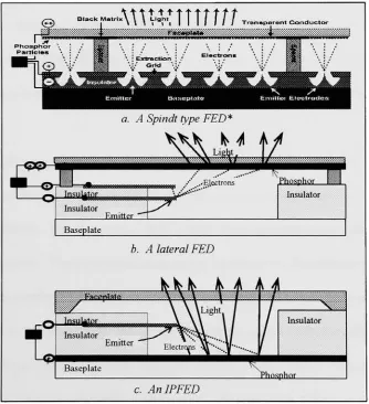
Figure
1
shows
three types
offield
emissiondisplay devices,
the
Spindt
type,
lateral
type,
and
lateral
type
withintegrated
phosphor.
The
oldestand
most commontype
of
FED
is
the
Spindt
type
of emitter(Fig.
la).
This
type
of
device has
been known for
30
years.
The
first
patentfor
such adevice
wasapplied
for in
19679.
Many
large
corporations,
including
Texas
Instruments, Motorola,
andMicron
Displays,
have
recently
invested
research
dollars in
this type
oftechnology.
The
Spindt
type
ofFED
is
characterizedby
a
conelike
cold cathode emitter withself-aligned
gate,
a
phosphorcoated
faceplate
acting
as
ananode,
and
high
aspectratio
Black Matri
AttM-TITTWf*-parentConductor
a.
A Spindt
typeFED
Insulator Emitter
Insulator
Baseplate
b. A lateral FED
m
Insulator
Baseplate
Phnsphnr
c.
An IPFED
Fig.
1-(a.)
A Spindt
type
FED.
(b.)
A lateral Field
Emission
Device.
(c.)
An Integrated
Phosphor
Field
Emission
Device (IPFED).
[image:17.614.147.481.326.692.2]spacers
to
separate
the
faceplate
andbaseplate.
The
faceplate
and
baseplate
are
fabricated
separately,
then
joined
at
the
end ofthe
process.
The
second
type
ofFED
is
the
lateral
type
(Fig.
lb).
This
type
ofFED
is
characterized
by
a
lateral,
thin
film
cathode and
gate,
phosphor coated
faceplate
whichacts as
ananode,
and
high
aspectratio
spacer columns.As
withthe
Spindt
type
ofdevice,
the
baseplate
and
faceplate
arefabricated
separately
then
joined
at
the
end
ofthe
process.
The
third type
ofFED
-the
one
whosefabrication is detailed in
this thesis
is
similar
to the
lateral
device, but,
as canbe
seen(Fig.
lc),
there
is
no phosphor coatedfaceplate
orhigh
aspect
ratio spacer columns.Instead,
the
phosphoris integrated
directly
into
the
device.
This
type
ofdevice is
referred
to
as anintegrated
phosphorfield
emissiondevice
(IPFED).
All
three
devices
must maintain ahigh
vacuum(1X10⁶
to
1X10"7 ton*)12in
the
active area
between
the
cathode andanode
for
the
lifetime
ofthe
device
(much like
a
CRT)
Most
phosphors
usedin Spindt
andlateral
type
field
emissiondisplays
arepowdered
phosphors,
eitherdeposited
by
settling,
orby
electrophoresis
ona
screen(the
faceplate
of aFED).
This
faceplate is
then
bonded
some
distance
away from
the
cathode
containing
baseplate.
The
separationbetween
the
baseplate
andfaceplate is
accomplished
by
using
non conductive spacercolumns.
These
columnsneed
to
be
smallenough so
they
are
not
visibleto the
nakedeye,
but strong
enoughto
support
the
phosphor screen and
maintain
the
properspacing between
the
cathode and anode.
This
is
no
smalltask
sincethe
area
between
the
plates
is
underhigh
vacuum.Assuming
14.7
lbs.
persquare
inch
ofatmospheric
pressure,
a
6"by
6"Spindt
type
display
screen would exert
530
pounds
ofThe
height
ofthe
spacercolumns
is
onthe
order oftens
to thousands
of microns.The
columns
are
subject
to
bombardment
by
electrons
from
the
emitters.This
bombardment
generates
secondary
electronsfrom
the
columns,
and
tends
to
positively
charge
the
columns.The
charging
then
exacerbatesthe
electronbombardment.
Eventually,
a
momentary
short
is
producedfrom
the
phosphor screento the
emitters viathe
columns,
rendering
the
Spindt
type
display
inoperative.
The
electronbombardment
ofthe
columns
willalso
cause
heating
ofthe
columns
and phosphors whichleads
to
outgassing
anddegradation
ofthe
high
vacuum.The
heating
and
charging
of spacercolumns
is presently
a major problemin FEDs
which utilizethem.
Some
researchershave
gone as
far
asto
abandon spacersby increasing
the
thickness
ofthe
faceplate
glass.This
solution solves
the
spacerproblems,
but
makes
their
displays
heavy
and unsuitablefor
portable
devices.
Field
emissiondevices
whichemploy
spacer columntechnologies
have
a
difficult
area
to
evacuate and
keep
underhigh
vacuum.As
willbe
discussed,
there
is
arelatively
small
Z spacing
between
the
baseplate
and
faceplate
whencompared
to the
X
and
Y
spacing.
As
mentioned,
field
emissiondevices
needto
operatein
a vacuum onthe
orderof
lxlO"7
to
lxlO"10torr.
The
large,
narrow spacesbetween
the
baseplate
andfaceplate in
FEDs
with spacercolumns make
this
level
of vacuumdifficult
to
maintain.IPFED
devices
possess
only
avery
small areasto
evacuate.Each IPFED
pixelresides
in
its
own microvacuumchamber and
has
its
ownprivate getter.
Due
to the
currentfluctuations
and
generally
unpredictablebehavior
ofSpindt
type
emitters, the
general practiceis
to
utilizemany
emittertips to
light
up
a single pixel.The
appropriate
vacuumin
aSpindt
type
device
it
is
necessary
to
evacuate
the
large,
narrowarea
between
the
screen and
emittertips.
This
is generally
accomplishedby
first
pumping
the
space
to
remove most
ofthe
gases,
sealing
the
area,
then
using
a
suitable getter atthe
edge of
the
screento
maintainhigh
vacuum.The
problem
withgettering in Spindt
andlateral FEDs
is
that
in
orderfor
a gasmolecule
to
be
gettered,
it
must
diffuse
allthe
way
to the
edge ofthe
display.
This
distance may be many
centimeters,
and as
indicated,
the
diffusion
ofthe
gasesis inhibited
by
the
smallZ spacing
between
the
baseplate
and
faceplate.
In
anIPFED
device
the
areawhich
needs
to
be
evacuatedis
very
small.
From
a
vacuumstandpoint,
each pixelis
isolated
from
the
next.Each
pixelhas
its
own private getter.The diffusion distance
ofresidual
gas molecules
in
anIPFED
is
many
orders of magnitudeless
than
in
FEDs
withspacercolumn
technologies.
Less
diffusion
time translates
into less
opportunity
for
these
residual gas molecules
to
adsorb on emittertips,
which can "poison"the
emittertips
by
changing
the
emittertip
workfunction,
thus
causing fluctuations in
the
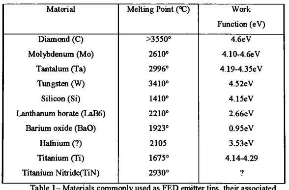
emission current.Material
Melting
Point(C)
WorkFunction
(eV)
Diamond
(C)
>35504.6eV
Molybdenum
(Mo)
26104.10-4.6eV
Tantalum
(Ta)
29964.19-4.35eV
Tungsten
(W)
34104.52eV
Silicon
(Si)
14104.15eV
Lanthanumborate
(LaB6)
22102.66eV
Bariumoxide
(BaO)
1923 0.95eVHamium
(?)
2105 3.53eVTitanium
(Ti)
16754.14-4.29
Titanium
Nitride(TiN)
2930 ?Table1-Materials commonlyused asFEDemitter
[image:20.613.163.457.528.721.2]2.2
Fowler-Nordheim
Tunneling
As
mentioned,
alltypes
of
field
emissiondevices
are governedby
Fowler-Nordheim
tunneling.
Fowler-Nordheim
(FN)
tunneling
is
a
quantum mechanicalprocess
by
which alow
workfunction
material - suchas
tantalum,
molybdenum,
lanthanum
hexaboride,
carbon,
ordegenerately
doped
silicon-tunnels
electronsthrough
a
barrier
under
the
influence
ofa
strong
electric
field.
Table
1
contains
the
workfunctions
ofsome common cathode materials.
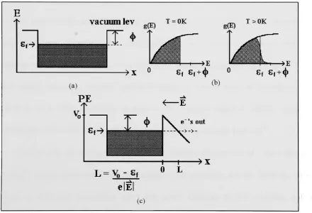
In solids,
at zerodegrees
Kelvin,
conductionelectrons are
confinedin
a potentialwell.
Electrons fill
allenergy
states
up
to the
fermi
energy
level
atthis temperature.
In
a
vacuum
lev
t
=ok
f^
T>0K
i >E
8f f
+<()
PE
v0
Sf-(c)
Fig
2*-(a)
Conduction
electrons confinedin
a potential well at0K. The
workfunction,
<j>,is
theenergy
required
by
an electronto
escape the potential well,(b)
Density
ofstatesfunction
as afunction
oftemperature.
At
elevatedtemperatures
thereis
anincreased probability
some ofthe
electronswillescapethe
potential well,(c)
Conduction
electrons confinedin
apotential well underthe
influence
ofahigh
electric
field.
The
electrons cantunnel through the
potentialbarrier
sinceit is bent
by
the
field. The
[image:21.614.87.527.350.650.2]vacuum,
the
minimum
energy
required
to
remove
an electronfrom
the
potentialenergy
well
is
the
material's
workfunction
"<{)"
(see
Fig
2a).
Work
functions
canvary
from
leV
up
to
5.6eV
for
most metals.
At
temperatures
above0K,
the
probability
that
someelectrons
willhave
enough
energy
to
escape
the
potentialenergy
well of a solidincreases
(Fig. 2b).
This
is
the
principlebehind
a
traditional
hot
cathode
filament
such asthat
found in
acathode
ray
tube.
This
type
of emissionis known
asthermionic
emission andis
characterized
by
ahot
cathode.Fowler-Nordheim
tunneling
does
not requirea
hot
cathodeto
allow electronsto
tunnel
out
ofa material's potential
energy
well.This
is
one
ofits
majorbenefits.
High
electric
fields
are
usedto
distort
the
potentialenergy
well.Electrons
atthe
Fermi energy
level
canthen tunnel
out ofthe
potentialenergy
well(Fig
2c).
The
advantages ofFowler-Nordheim
tunneling
overthermionic
emission arethat
quantum mechanicaltunneling
requires zero powerto transfer
electronsinto
avacuum, there
is
no needto
spend
energy
heating
acathode,
andfield
emission sources arenot
dependent
onthe
crystalline state
(The
exceptionto this
is
the
negative
electronaffinity
supposedly
exhibited
by
<1
1
1>
SP3diamond7)
and perfection ofthe
cathode
material10
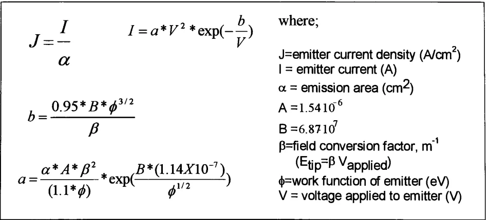
Shown
(Fig.
3)
are
the
equations
whichdescribe
the
process
ofFowler-Nordheim
tunneling11
From
these
equationsit is
apparentthe
tunneling
current
from
the
cathode
(emitter)
is
notonly
dependant
uponthe
workfunction
ofthe
cathode,
but
also
exponentially
dependant
uponthe
electric
field
atthe
tip
ofthe
cathode.
For
aFED
device
without
a
control gate(a
FED
diode),
the
electricfield is dependant
uponthe
voltageapplied
between
the
anodeand
cathode,
the
distance between
the
anode and
cathode,
and
inadvertently
(from
alarge
metal grain orprocessing abnormality),
will enhancethe
field
atthat
point on
the
emittertip(cathode).
If
the
I-V
characteristics
ofa simple
Fowler-Nordheim
diode
are plotted
ln(I/V2)
vs.
1/V,
where
I
is
the
current emitted
from
the
cathode
andV
is
the
voltagebetween
the
cathode
and
anode,
the
plot should
yielda straight
line
witha
slope proportionalto
the
work
function
ofthe
cathode raisedto the
3/2
power12.This
plotis known
asthe
Fowler-Nordheim
plot
andis
the
classic
test
for
Fowler-Nordheim
emission11Holding
all otherfactors
constant,
the
lower
the
workfunction
ofthe
cathode,
the
higher
the
cathode
emissioncurrent
willbe.
A
table
listing
common cathodematerials,
their
workfunctions,
andmelting
points
in
shown(Table
1).
Any
atomic species whichare adsorbed on
the
surface ofthe
cathode,
however,
can changethe
cathode's workfunction.
Atomic
adsorptionhas been
shownto
effect
the
workfunction
ofmaterials
by
as much as
25-50%12
Simple
calculations
using
the
equations
in Fig.
3
indicate
a25%
increase in
cathode workfunction
translates
into
adecrease
in
emittercurrent
density
ofj=
s,*T/2 *b
I
=a*V'*exp(
)
V
a
b
= 0.95*B*f21
a-
a*A*/3\
B*(LUX10-7)
(1.1*0
<binwhere;
J=emitter
current
density (A/cm2)
I
=emitter current
(A)
a =emission area
(cm^)
A=1.5410~6
B
=6.87107
p=field
conversion
factor,
m"1(Etip=pVapp|jec,)
<|>=work
function
of emitter
(eV)
V
=voltage
applied
to
emitter
(V)
[image:23.613.67.543.494.709.2]approximately 3300%.
A 50%
decrease
in
cathode workfunction
translates
into
anincrease
in
emittercurrent of
125,000%.
For
this
reasonit
is
necessary
to
operatefield
emission
devices
in
a
vacuum.The
higher
the
vacuumthe
better,
but
a
pressure of 1X10'torr
is minimally
acceptable.
There
are
benefits
to
operating
a
FED
in
a
vacuum otherthan
keeping
the
cathodesurfaces clean.
A FED
will produce nolight
without a phosphor.Several
ofthe
phosphors
used willabsorb moisture
from
the
air anddegrade
performanceif
precautionsare
nottaken.
The
vacuum will prevent waterabsorption.
Also,
The brightness
ofthe
phosphor
depends
uponhow
muchenergy
the
electronspossess
whenit
collides withthe
phosphor.
If
there
aregas
molecules
between
the
electronemitting
cathode andthe
phosphor
anode,
the
electrons
willlose
energy
in
collisions withthe
gas molecules.But,
more
importantly,
a
high
vacuum will prevent gasesbetween
the
anode and
cathodefrom
being
ionized.
Ionized
gases
willbe
acceleratedby
the
high
fields
presentin
aFED
andwill
begin
to
sputterthe
cathode.Sputtering
ofthe
cathode
willnegatively impact
the
emission properties of
the
device. As
long
as
the
distance between
the
cathode and
anodeis
much smallerthan
the
meanfree
path ofthe
electrons
emittedfrom
the
cathode,
there
will
be
no
ionization
of residualgases10
Atomic
scale
variations onthe
surface ofthe
cathode
willeffect
the
focusing
ofthe
electric
fields
at
the
cathodeand
willcause
significantly
different
emissioncurrents,
evenbetween
two
seemingly
identical
cathodes1.
If
these
smallvariations are
not present whenthe
FED
is
fabricated,
they
canbe built
up
overtime.
Electromigration
ofatoms
onthe
surface
of
the
cathodecan
occur underthe
presence of
the
high
electric
fields
utilizedin
cathode
atelevated
temperatures13.
As
mentioned,
FEDs
utilize a cold cathode.High
currentdensities
will cause
the
cathode
to
heat
up,
however,
and contributeto the
electromigrationin
the
devices.
2.3 Failure in FEDs
Resistance
heating
is
one ofthe
mechanismsfor failure in
FEDs. If
there
is
amomentary
spike
in
cathode emission currentdue
to
eitherthe
adsorption of somelow
workfunction
atomicspecies,
orthe
formation
of afield
enhancing
bump by
electromigration, the
cathode canbe
damaged
ordestroyed from
the
high
currentdensities
produced.Disruption
of emittersgenerally
occurs when
the
hottest
part ofthe
emitter approachesthe
melting
point ofthe
material of whichit
is
composed11.This
conditioneventually
causesmelting
or gassification ofthe
emittertip
(Fig
4).
Fig. 4
-A
Spindt
type of emitter
tip
whichhas been
melteddue
tohigh
currentdensities
and theresulting
resistance [image:25.614.166.446.430.695.2]Current
spikes
in FED
emitters
are reducedby
reducing
emittertip
adsorptionand
electromigration
in
additionto
one
orboth
oftwo
supplementary
methods.The
first
method
is
a
two
step
process.
First,
afield is induced
atthe
cathode whichis
strong
enough
to
bring
about
Fowler-Nordheim
tunneling.
Then,
the
emission currentis
controlled
via acurrent
limiting
circuit.The
second
methodis
to
incorporate
a resistivelayer in
series withthe
cathode.
Each
cathode
canhave its
owndiscrete
resistor14
or
a
single resistive
layer
can
be
usedto
contact
many
cathodes15
The
resistivelayer
willreduce
the
averagecurrent spike
to
whereit is
small enoughnot
to
damage
the
emittertip.
Chapter
3
IPFED Devices
vs.Other Types
ofFEDs
All
ofthe
FEDs, Spindt,
lateral,
andIPFED,
have
the
advantages of a wideviewing angle, very
fast
responsetime
allowing for
the
display
offast moving
videosignals,
a widetemperature
range(-45C
to
85C),
and
bright,
colorfuldisplays
andhigh
portability
since eventhe
largest FED
is less
than
V4"thick
.The
widetemperature
rangestems
from
the
fact
the
devices
arecompletely
solid state.The
bright,
colorfuldisplays
are
due
to the
fact
that
FED
phosphors arevery
similarto
those
usedin CRTs.
Field
emission
displays
have
many
advantages
overcathode
ray
tubes
andactive matrix
liquid
crystal
displays.
Integrated
phosphorfield
emissiondisplays have
advantages
overthe
Spindt
andlateral
types
offield
emissiondisplays.
It
has
already
been
mentionedthat
each pixel of anIPFED
is isolated
from
oneanother
from
a vacuum standpoint.Also,
each pixelhas
its
ownactive
getterto
maintaina
high
vacuum within eachpixel.
For
these
reasons,
residualgas molecules
have
agreater
current
fluctuations.
This
is
a
huge improvement
over othertypes
ofFEDs
which usespacer
columntechnologies.
3.1
Anode
to
Cathode Distance
Another
advantage
of anIPFED
is
that the
anode
to
cathode
spacing
(and
cathodeto
gate
spacing
if
one
is
included)
is
nonphotolithographically defined.
The spacing
is
defined
by
the thickness
ofthe
chemically
vapordeposited
(CVD)
thin
film
insulating
layer,
whichseparates
the
cathode and anode.
Since
the thickness
ofCVD
films is
aneasy
parameter
to
controland
keep
under controlin
amanufacturing environment,
the
anodeto
cathode
spacing
is likewise easy
to
control.
Since
cathode
emission currentis
dependant
upon
the
electric
field between
the
cathode
and anode andthe
electric
field
is
dependant
upon
the
potentialdifference
and
distance between
the
cathode
andanode,
distance is
acritical parameter
to
control.The
anode
to
cathode
(A-C)
spacing in
anIPFED
is
orders
ofmagnitude
less
than
in Spindt
orlateral FEDs.
A
typical
Spindt
orlateral
FED
may have
ananode
to
cathode(A-C)
spacing
of50
to two thousand
microns.IPFEDs
canbe fabricated
withspacings
ofless
than
0.1
urn althoughspacings
of~0.75nmare more common.
Since
electric
field is
highly
dependant
uponthe
A-C
spacing,
anIPFED's
reducedspacing
translates
into
lower
operational voltage.From
an operational voltagestandpoint,
the
use of a controlgate
in Spindt
andlateral FEDs
makesup
for
their
increased
A-C
spacing.
Other
advantages
resulting
from
reduced
IPFED
A-C
spacing
are still realized
however.
The IPFED 's
reduced
A-C spacing
makesthe
meanfree
path ofthe
electronsemitted
from
the
cathode
less
important.
In
allFEDs,
a
high
vacuummust
be
maintainedto
keep
cathode surfaces
clean,
phosphors
from absorbing
moisture,
and
to
reducethe
risk
of
the
emitted electrons
ionizing
residualgases
withinthe
device.
In
an
IPFED,
the
A-C
spacing
is
so
small,
evenat
higher
pressures
there
is little
risk
ofstriking
a
plasmabetween
the
anodeand
cathode.
A
high
vacuum must stillbe
maintainedfor
the
othertwo
aforementioned
reasons.As
canbe
seen(Fig.
1),
when electrons are emittedfrom Spindt
andlateral
FEDs,
the
electrons strikethe
bottom
ofthe
phosphors coated onthe
faceplates.
Electron
penetration
depths
atlow
voltages(less
than
500
V)
are onthe
order of afew
tens
ofnm16
This
means visible photons which are producedby
cathodoluminescence musttravel
through
the
bulk
ofthe
phosphor,
then through the
faceplate
glass
in
orderto
reachthe
eye.
Some
ofthe
photons willbe lost
during
this
process.Electrons
emittedin
anIPFED
device
strikethe
top
ofa
thin
film
phosphorcausing
it
to
cathodoluminesce.Photons
produced
by
this
cathodoluminescencetravel
through
avery
thin
(<l^m)
layer
ofencapsulation
glass,
then
are visibleto the
eye.There
is
very
little
possibility
for
attenuation.
Thus,
the
light
producedis
much moreefficiently
utilized.3.3 FED Phosphors
A
thin
film
phosphor withoutany
sulfuris
usedin
IPFED
devices.
A
powdered
phosphor
is
usedin Spindt
and
lateral FEDs.
Powdered
phosphors
have
very
large
grainsizes
(greater
than
l\im).
These
phosphors are coated
onthe
faceplates
ofSpindt
andwithin
the
vacuumdisplay
area.Sulfur
is
a
material which wreakshavoc
withthe
emissionproperties
ofFED
cathodes7
If
there
is
sulfurin
the
powderedphosphor,
andbecomes
free due
to
electron
stimulation anddecomposition,
there
is
a
very
good chanceit
willadsorb
onthe
emittersurface,
drastically
changing
the
emission characteristics ofthe
device.
This
is
a
reliability
problem.
The
IPFED
which wasfabricated in
this
thesis
utilizes a
thin
film
phosphorconsisting
ofzinc,
tantalum,
and oxygen.The
material wasdeveloped
at
the
Rochester
Institute
ofTechnology
and wasfirst
reported onin
November
ofl99616
The
phosphor utilizedin
the
IPFED
device
is
Ta2Zn308
andis known
astantalum
zinc
oxide
(TZO).
TZO
is
a cathodoluminescent
phosphor witha
spectral peakat
410nm.
The
cathodoluminescence
is
visible at10V
of electron acceleration voltage ata
currentdensity
ofThe chromaticity
(CIE)
coordinates are x =0.160,
y
=0.075.
These
coordinates correspondto
adeep
blue
color.The
films
are preparedby depositing
thin
film
tantalum
on r.f sputtered zincoxide
films
then
annealing
at
high
temperatures.
Both
ofthese
steps are standard semiconductor processes.The
advantages ofusing
a
thin
film
phosphorin
the
device
aretwofold.
First,
the
thin
film
phosphors canbe deposited
by
standard semiconductorprocessing
techniques.
A
sputterer,
appropriatetarget,
andprocess
are
allthat
arerequired
to
incorporate
the
phosphor within
the
IPFED
device.
Powdered
phosphors,
onthe
other
hand,
require
special electrophoretic
deposition
orsettling
equipment.This
is
a
messy,
inexact
process.In addition,
the
grainsize
ofthe
powdered phosphors
(>l^m)
make
incorporation
ofthe
do
not suffer
from
the type
of adhesion problems powdered
phosphorsdo.
There
is
little
chance
the thin
film
phosphor
willflake
off,
causing disruption
ofthe
IPFED
device.
Refractive
trapping
is
a process
in
whichphotons generated
in
thin
film
phosphorsare not emitted
directly by
the
surface of
the
thin
film
phosphorbut
are"piped"
to
and
emitted
from
the
edges of
the
material.
Refractive
trapping
in
a
thin
film
phosphoris
similar
to
what
happens
to
light
in
a
fiber
optic
cable.The
net result
of refractivetrapping
is
reduced
phosphorefficiency.
Tantalum
zinc oxidedoes
not sufferfrom
any
refractivetrapping.
Chapter
4 Previous Work
Related
to the
Fabrication
ofIPFEDs
Much
workhas been
reported whichis
usefulin
the
design
of a manufacturableprocess
flow for
anIPFED
device.
Before
the
wideacceptance
ofthe
modernsemiconductor
transistor,
vacuumtubes
ruled
the
electronics
industry.
Some
ofthe
most
basic
work oncold cathode
field
emission wasmade
in
aneffort
to
shrinkthe
size ofvacuum
tubes.
Modern
researchin
this
area continues
to
progress
in
an effortto
producea radiation
hard,
temperature
insensitive,
three
terminal,
transistor
like device.
Much
ofthe
exploration performed on vacuumtubes
has benefited
the
IPFED
researchperformed
in
this thesis.
Further,
the
workpresented
in
this thesis
may
benefit
the
vacuumtube
effort,
since anIPFED
is really
a cold cathode
vacuumtube
withan
integrated
phosphor.
An
excellent source of
information
for
this thesis
comes
from
researchperformed
on
Spindt
type
display
devices.
There
arepresently
two
competing
Spindt
type processes;
the
metal
microtip
process and
the
siliconmicrotip
process.Molybdenum
microtips
werefirst
usedby Capp
Spindt
andhis
coworkers
atSRI
international
and are still a core
FED
technology7The
fabrication
process
ofthe
baseplate
for
this type
oftechnology
is
shown(Fig.
5a). Note
this
is
an oversimplified processflow
showing
only
the
formation
ofthe
Spindt
tips.
It
does
not
include
the
formation
ofthe
faceplate
northe
bonding
and
vacuumsealing
ofthe
faceplate
andbaseplate.
The
processrelies on
the
eventual closure of a smallhole
etchedthrough
the
insulator
andthe
corresponding formation
of apointed
tip
below it.
The
pointedtip
becomes
the
field
emission cathode and
the
surrounding
layer,
whichis
electrically
isolated from
the
tip,
becomes
the
controlgate.
Other
processes
for
the
fabrication
of metalmicrotips
have
been
developed
but
they
allrely
onthe
closure
methodto
form
the
tips.
Materials
otherW(
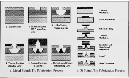
1.Basic Structure
_ _
,. , 3. SihcaEtchmg
2.Photamaskingand ., . . * tutu- r l ChenucalorEH RTT Processofthe
Gate. rJS^
4.VacuumDeposition 5. \acuumDeposition 6.Elettrodieiital
Etching
ofParting
Layer ofMirrotijs oftheParting
LayerThermal Oxidation
Mask Formation
Silicon Etchlii*
Thermal Oxidation
Insulatorand Gat*Metal
Deposition
Gate Formation
a.
Metal Spindt
Tip
Fabrication
Process
b. Si Spindt
Tip
Fabrication Process
Fig.
5
[image:31.614.99.518.468.721.2]than
molybdenum
have
also
been
used,
but
atthe
momentMo
is
the
dominant
materialfor
microtips
formation.
The
metal
microtip
process
utilizes severalhundred
emitters
per pixelto
improve
the
yieldand
reliability
ofthe
display.
Using
the
metalmicrotip
technology,
a sixinch,
low-voltage
colorprototype
display
has
been
fabricated
by
LETI
ofFrance,
in
collaboration
withPixTech
corporation.
A
key
aspect ofthis
prototype wasthe
incorporation
ofa
resistive
layer
to
provide
series resistorsfor
the
microtips.As
mentioned
previously,
the
resistors
limit
the
load
in
the
circuit and prevent
catastrophictip
failure.
The
second
type
ofSpindt
technology
is
the
siliconmicrotip.
The
processflow for
the
fabrication
ofthis type
ofmicrotip is
shown(Fig.
5b).
Again,
this
processflow
showsthe
steps
necessary only
to
fabricate
the tips
and
does
not
include
the
fabrication
ofthe
faceplate,
spacers,
bonding,
nor vacuumsealing
ofthe
display.
In
the
siliconmicrotip
process, atomically
sharp
points are
formed
by isotropically
etching
<111>
silicon.This
means,
ofcourse,
that
single
crystal silicon substrates needto
be
used.A
self-aligned
emitter process which eliminates several process steps exists.
This
technology
offsets
the
cost
for
the
single
crystal siliconsubstrates7
Micron
Display Technology
has
demonstrated
a
0.7
inch
color prototype
using
this technology.
Micron
is
ramping
up
for
production of
a one
inch
siliconSpindt
type
display.
4.2 Diamond-Like
Carbon
Cathodes
Another FED
technology
whichhas
receivedquite
abit
of attentionis
onethat
Austin,
TX
usesamorphous
diamond
patches asthe
electron emission siteinstead
of apointed
microtip
cone17.
Their
diamond is
laser
ablatedfrom
a graphite
target
viaa
pulsedNd:YAG laser.
Others
have
attempted
chemical vapordeposition
ofthe
diamond-like
carbon
using C2H2.
The
mechanism of emissionfrom diamond films is
not wellunderstood.
Calculation from
the
Fowler-Nordheim
equationgives
an effective workfunction
of0.2
to
0.3ev,
compared
to
about
4.5
eV
for Mo
and
Si
microtips7
It has
evenbeen
suggested
that the
diamond-like
carbonfilms
have
a
"negative
electron affinity".Laser
ablated
diamond is
microscopically
rough andforms
many
facets.
FED
pioneer
Henry
Gray
believes
that,
the
diamond
emitter'sgreatly
enhanced emission currentis due
to
reducedemitting
area and electricfield
focusing
ratherthan
anextremely
low
diamond
workfunction
orthe
novelidea
of"negative
electronaffinity"7
Whatever
the
mechanism,
diamond
emitters
do
exhibit
greatly
enhanced
emission currents andthus
a
bright
display
withoutthe
micromachining
inherent in
microtip
approachesis
possible.A
125X125
pixelmonochrome prototype
display
using
diamond
emissionpatches
has been demonstrated
by
SI Diamond. The
major problemthis
prototype
suffersfrom is
obtaining
uniform emission overthe
entire area ofthe
display7In addition,
the
prototype
device
presently
does
not
have
a
controlgate.
This
meansswitching
voltagesin
excess
of350V
are necessary.The
prototype
also
suffersfrom
powdered phosphor adhesionproblems.
The
prototype
uses a separatefaceplate
and
baseplate
along
withspacers
columns.
As
with all otherFED
technologies,
a
vacuumis
necessary for
stable
and
reliable operation.
Since
diamond is
a
very
inert film
however,
the
level
of vacuumrequired
is
muchless
than
competing FED
technologies.
This
technology
may be
well4.3
Other Reported
Research
onLateral
Emitters
Many
researchers
have fabricated
lateral field
emissiondevices for
a
widevariety
of applications
including
flat
paneldisplays,
microwave
devices,
field
emissionintegrated
circuits,
and magnetic sensors.
Kaneko
and
Sumita18fabricated
a
lateral
thin
film
star-likeemitter with an
incorporated
resistivelayer
underneath.The
processconcurrently
fabricates
a
Mo
orW
lateral
emitter witha
self aligned gate.The
result ofthe
incorporation
ofthe
resistivelayer is
a currentfluctuation
ofless
than
5%.
The
resistivelayer
adds
approximately five
mega-ohmsto
the
emission circuit.A
polysilicon resistivelayer is
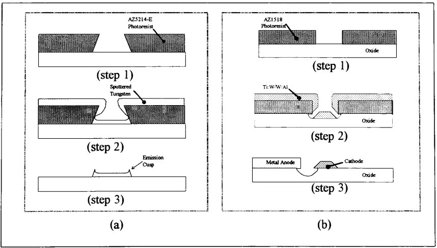
used.Kim
etal19
fabricate lateral
emitters out oftungsten.
The
thickness
oftheir
emitters
is
4000A,
but
they
fabricate
a point
ontheir
emittersin
a uniquemanor.
"Cusp
edge"
and
"knife
edge"
points are put
ontheir
emitters.The
processflow
usedto
produceAZ5214-E Photoresist AZI518 Photoresist
"1
\
(step
1)
! i(step
1)
^T
*y-y*(step
2)
Emission ^Cusp(step
3)
(a)
!
! : !I I
I 1 >i
i
Oxide
(step
2)
MetalAnode 1 >^^^-Cathode
^-
* Oxide(step
3)
(b)
Fig.6-
(a.)
Cusp-edge
cathodeformation
processfrom Kim
etal..(b.)
Knife-edge
[image:34.613.86.515.490.733.2]the
cusp
edge and
knife
edge emitters
is
shown(Fig.
6). Emission
characteristicsfor
these
devices
seemto
indicate
(by
virtue oftheir turn
ofvoltages)
that
Kim
et al.have
succeeded
in produci