Rochester Institute of Technology
RIT Scholar Works
Theses Thesis/Dissertation Collections
6-19-2006
Investigation of induced charge damage on
self-aligned metal-gate MOS devices
Robert Mulfinger
Follow this and additional works at:http://scholarworks.rit.edu/theses
This Thesis is brought to you for free and open access by the Thesis/Dissertation Collections at RIT Scholar Works. It has been accepted for inclusion in Theses by an authorized administrator of RIT Scholar Works. For more information, please [email protected].
Recommended Citation
Investigation of Induced Charge Damage on Self-Aligned
Metal-Gate MOS Devices
By
G. Robert Mulfinger
A Thesis Submitted in Partial Fulfillment
of the Requirements for the Degree of
Master of Science
in
Materials Science and Engineering
Approved by:
Prof. ________________________________ Dr. Karl D. Hirschman (Thesis Advisor)
Prof. ________________________________ Dr. Michael A. Jackson (Committee Member)
Prof. ________________________________ Dr. Andreas Langner (Committee Member)
Prof. ________________________________ Dr. K.S.V. Santhanam (Department Head)
DEPARTMENT OF MATERIALS SCIENCE AND ENGINEERING
COLLEGE OF SCIENCE
ROCHESTER INSTITUTE OF TECHNOLOGY
ROCHESTER, NEW YORK
Investigation of Induced Charge Damage on Self-Aligned
Metal-Gate MOS Devices
By
G. Robert Mulfinger
I, G. Robert Mulfinger, hereby grant permission to the Wallace Library of the Rochester Institute of Technology, to reproduce this document in whole or in part, with the knowledge that any reproduction will not be for commercial use or profit.
_________________ _________________
ABSTRACT
MOS capacitors and NMOS transistors were fabricated with various gate oxides and
inter- level dielectrics (ILDs) in order to study the effects of plasma induced charging
during the post- metal plasma deposition of an insulating oxide layer. The gate oxides
investigated include thermal SiO2, a low temperature oxide (LTO) deposited by low
pressure chemical vapor deposition (LPCVD) using silane and oxygen, and an oxide
deposited by plasma enhanced chemical vapor deposition (PECVD) using
tetra-ethyl-ortho-silicate (TEOS) as a precursor. A standard-recipe TEOS-based ILD was studied, as
well as an alternative recipe that utilized decreased power. Additional wafers were
fabricated with an LTO ILD to serve as a control group in order to isolate the influence of
the ILD deposition on the respective gate dielectric. By studying C-V and I-V
characteristics, both interfacial degradation as well as bulk charging was demonstrated as
a result of the PECVD ILD deposition. The investigation demonstrated clear differences
in plasma- induced charge effects on the various gate dielectrics. A correlation between
the ILD deposition power and the resulting charge influence was established. In addition,
post-plasma annealing experiments were done to study the thermal stability of induced
Table of Contents
Title Page……… i
Library Release Page………..……… ii
Abstract………...……… iii
Table of Contents……… iv
List of Figures……….……… vii
List of Tables………..……… x
1. Introductio n………...……… 1
1.1 Process Damage in High Temperature CMOS……… 1
1.2 Process Damage in Low Temperature CMOS……… 3
1.3 Motivation………...……… 4
2. Low and High Temperature Dielectrics………..……….. 5
2.1 Thermal Oxidation………..………..……….. 5
2.2 Chemical Vapor Deposition……….……….. 5
2.3 Dielectrics for Low Temperature Applications………..……… 8
2.4 Silicon Nitrides………..………. 8
2.5 PECVD Oxides……….……….………. 10
2.6 Multiple Layer Stacks………..………..………. 13
3. Experimental Techniques……….……… 15
3.1 Capacitance Measurements……… 15
3.2 Capacitance-Voltage Measurements……….. 15
3.3 Interface Trap Dens ity Distribution Measurements……… 19
3.5 Mobile Ion Measurements……….. 22
3.6 Current-Voltage Measurements……….. 23
4. Plasma Induced Charge Damage……….………. 24
4.1 Introduction………. 24
4.2 Electron and Hole Trap Generation……… 26
4.3 Oxide Traps and Gate Leakage……….. 28
4.4 Assessment of Plasma Induced Charge Damage……….……….. 29
5. Experimental Design and Device Fabrication……….. 31
5.1 Capacitor Experimental Design………. 31
5.2 Capacitor Fabrication………. 31
5.3 Transistor Experimental Design………. 33
5.4 Transistor Fabrication………. 34
6. Capacitance-Voltage Analysis……….. 51
6.1 Preliminary C-V Data……… 51
6.2 Mobile Ionic Contamination………....……….. 54
6.3 Stress-Induced Defects from TBS……….. 59
6.3.1 Stressing Oxides Annealed at 600°C……….. 59
6.3.2 Stressing Oxides Annealed at 600°C……….. 61
6.3.3 Interface Trap Densities……….. 63
6.4 Breakdown and Leakage Current Measurements……….. 65
6.5 Conclusions from Initial Capacitor Data……… 67
7. Investigation on Integrated Devices….……… 69
7.2 Reference Wafers with LTO ILD……… 71
7.3 Standard TEOS ILD Annealed at 600°C……… 73
7.4 Standard TEOS ILD Annealed at 900°C……… 76
7.5 Low Power TEOS ILD Annealed at 600°C……… 77
7.6 Low Power TEOS ILD Annealed at 900°C……… 80
7.7 Annealing Bulk Charge Damage in LTO Gate Oxides……….. 82
8. Conclusion……… 84
8.1 Susceptibilities of the TEOS Gate Oxide……….. 84
8.2 Susceptibilities of the LTO Gate Oxide………. 86
8.3 Susceptibilities of the Thermal Gate Oxide……… 87
8.4 Low Power VS. High Power ILD Deposition……… 88
8.5 Closing Remarks……… 88
List of Figure s
Fig. Description Page
1.1 Cross-section of a Modern NMOS Transistor………. 2
1.2 Typical Bottom gate TFT processed at low temperatures…………...……. 3
3.1 Circuit diagram of capacitance-conductance meter………..……. 15
3.2 Accumulation, Depletion and Inversio n (P-type)……….……. 16
3.3 Dit for TEOS SiO2 capacitor by Kuhn Method………....……. 20
3.4 Breakdown Measurement………. 21
4.1 Direct band-to-band tunneling and Fowler-Nordheim tunneling…………. 25
4.2 HDP Model for Hole Trapping………. 27
4.3 Electron and Hole Trap Generation and Annihilation Processes…………. 28
5.1 Cross-section of Capacitor Fabrication………. 32
5.2 Cross-section of P-well and pad oxide formation………. 35
5.3 Back Side Contact Implant……… 36
5.4 Field Oxide Deposition………. 36
5.5 Active Lithography……… 38
5.6 Active Etch and Resist Strip……….. 39
5.7 Gate Oxide Deposition………...……. 40
5.8 Molybdenum Gate Deposition……….. 41
5.9 Gate Lithography……….. 41
5.10 Cross-section after gate etch and resist strip……….. ….. 42
5.11 Cross-section of screen oxide deposition………. 43
5.13 ILD Deposition………. 44
5.14 Contact Lithography………..…… 45
5.15 Contact Etch and Resist Strip……… 46
5.16 Aluminum Deposition………... 46
5.17 Aluminum Lithography………... 47
5.18 Aluminum Etch and Resist Strip……….. 48
5.19 Capacitor Lithography……….. 48
5.20 Capacitor Etch and Resist Strip……… 49
5.21 Final Device Cross-section……… 50
6.1 C-V Curves of LTO, TEOS and Thermal Oxides………. 51
6.2 Initial Interface Trap Density Distributions……….. 53
6.3 TBS data for LTO Annealed at 600°C……….. 54
6.4 TBS data for TEOS Annealed at 600°C………... 54
6.5 TBS data for Thermal oxide……….. 54
6.6 TVS Data for Oxides Annealed at 600°C………. 55
6.7 TVS Data for Oxides Annealed at 900°C………. 56
6.8 TVS Data for TEOS with no Anneal……….. . 57
6.9 TVS Data for Annealed and Un-Annealed……….. . 58
6.10 C-V Curves Before and After Stressing Oxides Annealed at 600°C……... 60
6.11 Decrease in Maximum C-V Slope for 600°C oxides………... 60
6.12 C-V Curves Before and After Stressing Oxides Annealed at 900°C……… 61
6.13 Decrease in Maximum C-V Slope for 900°C oxides……… 62
6.14 LTO Oxide Dit Before and After Stress………... 63
6.16 Thermal Oxide Dit Before and After Stress………. 64
6.17 Increase in Dit after Stressing for TEOS, LTO and Thermal Oxides…….. 65
6.18 Breakdown Plots of LTO, TEOS and Thermal Oxides……… 66
6.19 Leakage Currents of LTO, TEOS and thermal oxides………. 66
7.1 C-V curves of Integrated LTO Oxide Capacitors……….. 69
7.2 C-V curves of Embedded TEOS Oxide Capacitors……….. 69
7.3 C-V curves of Embedded Thermal Oxide Capacitors……….. 70
7.4 Linear ID-VG Curves for Devices with LTO ILD (VD=0.1V)………... 71
7.5 Saturation ID-VG Curves for Devices with LTO ILD (VD=10V)………….. 72
7.6 Linear ID-VG Curves for Devices with Std. TEOS ILD (VD=0.1V)……….. 73
7.7 Saturation ID-VG Curves for Devices with Std. TEOS ILD (VD=10V)……. 74
7.8 Sub-threshold Swings for Devices with TEOS and LTO ILD’s………….. 75
7.9 Oxidation of the Molybdenum Gate………. 77
7.10 Linear ID-VG for Devices with Low Power TEOS ILD (VD=0.1V)………. 78
7.11 Saturation ID-VG for Devices with Low Power TEOS ILD (VD=10V)…… 78
7.12 Sub-Threshold Swings- LPTEOS and LTO ILDs………. 79
7.13 Linear ID-VG for Devices with Low Power TEOS ILD (VD=0.1V)…….… 80
7.14 Saturation ID-VG Curves with Low Power TEOS ILD (VD=10V)………… 81
7.15 Sub-threshold Swings-LPTEOS 600°C/900°C……….… 81
7.16 Linear ID-VG Curves for Devices with Std. TEOS ILD (VD=0.1V)…….… 82
7.17 Saturation ID-VG Curves with Std. TEOS ILD (VD=10V)……… 83
8.1 I-V Data Summarized for the TEOS Gate Oxide……….… 85
8.2 I-V Data Summarized for LTO Gate Oxides……… 86
List of Tables
Table. Description Page
2.1 Comparisons of APCVD, LPCVD and PECVD……….. 8
5.1 Capacitors Fabricated………..…. 32
5.2 Transistors Fabricated……….………. 34
6.1 Total Oxide Charge Data………. 52
CHAPTER 1
INTRODUCTION
1.1
Process Damage in High Temperature CMOS
Since Jack Kilby’s invention of the integrated circuit in 1958, the size of the field
effect transistor has shrunk drastically in order to provide increasing computing power for
modern day devices [1]. As transistor sizes continue to decrease, the gate oxide becomes
increasingly more susceptible to process induced damage. When plasma is used in
various fabrication steps, localized charge build up creates significant electric fields that
produce tunneling current. Defects initiated by this tunneling current cause decreased
breakdown voltages, increased interface states, increased leakage current, deteriorated
oxide reliability and even decreased yield as oxides can break down during processing
[2]. To meet scaling demands, gate oxides are now reaching thicknesses approaching
12-15Å [3]. As a result of this, the effects of plasma process induced damage are becoming
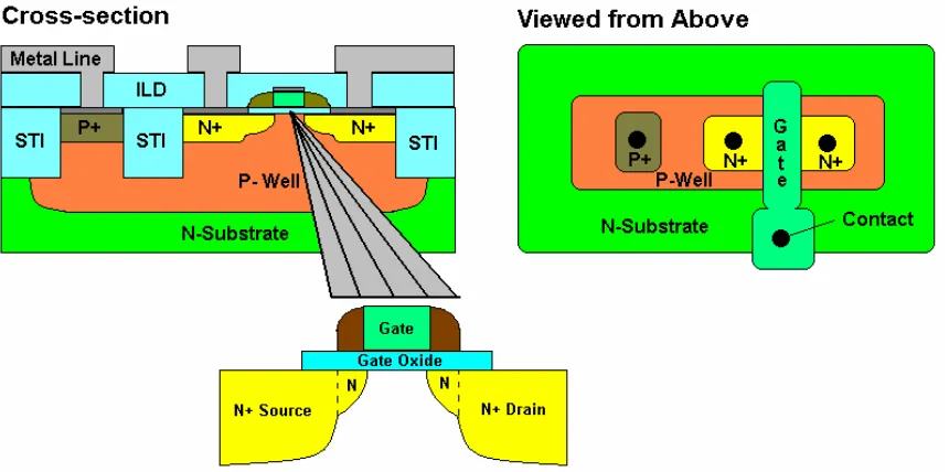
an increasing concern. Figure 1.1 shows a typical modern day NMOS device that might
Figure 1.1: Cross-section of a modern NMOS transistor
Normal operation of the device would consist of grounding the source and applying a
positive bias on the drain and gate. As the voltage on the gate increases, electrons from
the boron-doped (p-type) well accumulate beneath the gate oxide to form an inversion
channel. Subsequently current flows from the source to drain and the device is
considered to be on. When an ultra-thin gate oxide is broken or severely degraded during
plasma processing, current flows from the source directly through the oxide reaching the
gate. When this happens the gate loses complete control over the source to drain current
and the device is rendered useless.
The device shown in Figure 1.1 is fabricated on bulk silicon wafers, where thermal
constraints are relatively relaxed. This means that the devices can be processed at higher
temperatures (above 900°C) without causing structural damage to the substrate. In most
cases, this can allow for a significant portion of process- induced damage to anneal.
Fortunately, the majority of integrated circuit applications use devices fabricated on a
[image:13.612.111.541.73.287.2]1.2
Process Damage in Low Temperature CMOS
Low temperature processes are specifically of interest in the area of Thin Film
Transistor (TFT) research. TFTs are used in applications such as liquid crystal displays
(LCDs) as a means of switching the pixels on and off. In order to transmit light for
displays, they must be fabricated on a clear glass or plastic substrate. As a result, thermal
constraints become more stringent in order to prevent the substrates from melting or
deforming during processing. This generally limits useable process temperatures to
below 600°C [4].
Since low temperature CMOS processes are done below 600°C, thermal oxides
cannot be practically grown and used as gate dielectrics, as in standard technology. Low
temperature oxides (LTO) or silicon nitrides are needed as gate dielectrics because of
this. Dielectrics deposited at lower temperatures (compared to a thermal oxide) exhibit
structural inferiority resulting in higher leakage currents and lower breakdown strengths.
These effects are directly correlated with plasma induced charging. Furthermore, low
temperature CMOS processes are limited in the ability to anneal out this damage, leaving
devices even more vulnerable to process induced degradation. Figure 1.2 shows a typical
TFT that would need to be processed at low temperatures.
Despite being upside-down, the TFT shown above operates the same way as the transistor
in Figure 1.1. TFTs usually have a similar bottom gate design. The dielectric and
amorphous silicon are then deposited on top of the gate. This configuration saves a
lithography step that would ordinarily be needed to pattern for the source/drain implants;
the wafer is simply coated with resist and flood exposed through the transparent substrate
resulting the self-aligned source/drain pattern.
1.3 Motivation
RIT has been developing a low temperature TFT process to characterize a new
silicon-on-glass substrate material under development by Corning, Incorporated.
Because processing temperatures must be low, as dictated by the glass strain point [5],
and gate oxides are of inferior quality compared to a thermally- grown oxide, significant
effects of induced charge damage have been observed [26]. This work focuses on
characterizing such effects in deposited oxides using devices fabricated on bulk silicon
CHAPTER 2
LOW & HIGH TEMPERATURE DIELECTRICS
This chapter presents information on a variety of insulating materials that have been
implemented in industrial applications in order to meet the requirements of low
temperature processing constraints with acceptable dielectric performance.
2.1 Thermal Oxidation
Thermal oxidation is a well-known process that results in a durable, high quality film
with minimal charge levels. Most importantly, the interface between silicon and
thermally grown SiO2 contains less dangling bonds and interface-trapped charge as
compared to deposited dielectrics. For such applications, as thin film transistors that
require process temperatures below 600°C, it is not practical to use an
atmospheric-pressure thermally grown oxide as the gate dielectric. While high-atmospheric-pressure oxidation can
be used to grow SiO2 to a practical thickness for this application, the film quality is
compromised significantly [6].
2.2 Chemical Vapor Deposition (CVD)
There are three main techniques used for CVD of dielectric materials for
semiconductor applications. This section describes the techniques, their applications, and
APCVD
Atmospheric Pressure Chemical Vapor Deposition (APCVD) is the simplest of
the various CVD deposition techniques. A predetermined mixture of reactant and
diluting inert gas is used to transport gas species in a reaction chamber to the substrate.
In such a CVD system there are two types of reactions that occur. First, what is called a
homogeneous reaction occurs in the reactor’s atmosphere. When this occurs, aggregates
of the material being deposited form in the gas phase and adhere to the surface of the
substrate forming low-density films with many defects. The second type of reaction that
occurs in the system is known as a heterogeneous reaction. In the heterogeneous
reaction, gas reactants are adsorbed on the substrate (which is heated) where they react to
form a high quality deposited film. This is, therefore, the favorable reaction in vapor
deposition. In an APCVD deposition, the reactions are limited by the amount of gas
reaching the surface, also known as being in the mass-transport- limited regime. After the
reactions occur, remaining gaseous by-products are then desorbed from the surface and
removed from the chamber [7].
LPCVD
Low Pressure Chemical Vapor Deposition (LPCVD) is very similar to APCVD.
The main difference is the decreased pressure. LPCVD is typically done at 0.25-2.0 torr
and temperatures between 550°C and 700°C. Because of the decreased pressure, films
are deposited in the reaction-rate- limited regime. At low pressure, diffusivities of
reactant gases are increased such that their transfer to the substrate doesn’t limit growth
which is dominated by temperature. Temperature control in LPCVD tools is very
accurate. Therefore, film uniformities of LPCVD films are superior to those deposited by
means of APCVD. Also, lower pressure decreases the unwanted homogeneous gas-phase
reactions. This results in higher quality films that have less contamination than those
deposited by APCVD [6].
PECVD
Plasma Enhanced Chemical Vapor Deposition (PECVD) is a deposition method
that uses plasma to excite reactive gases in order to help dissociate them at lower
temperatures. Two electrodes, one of which is the chuck holding the wafer, form the
plasma under a vacuum with regulated gas flow. Free electrons are accelerated in the
electric field causing both elastic and inelastic collisions with the gas molecules. The
inelastic collisions result in dissociation and ionization of the gas molecules as well as
secondary electrons. Dissociated gaseous ions utilize a heterogeneous reaction on the
wafer surface to form the deposited film [8].
Each of these deposition techniques has different advantages, disadvantages and
CVD ProcessAdvantages Disadvantages Applications
APCVD
Simple, Fast Deposition, Low Temperature
Poor Step Coverage,
Contamination Low -temperature Oxides
LPCVD
Excellent Purity, Excellent Uniformity, Good Step Coverage,
Large Wafer Capacity
High Temperature, Slow Deposition
High-temperature Oxides, Silicon Nitride, Poly-Si, W, WSi2
PECVD Low Temperature,
Good Step Coverage
Chemical and Particle Contamination
Low -temperature Insulators over Metals, Nitride Passivation
Table 2.1: Comparisons of APCVD, LPCVD and PECVD [7]
2.3 DIELECTRICS FOR LOW TEMPERATURE
APPLICATIONS
This section describes physical and electricdal properties of various gate dielectrics
that ha ve been used in low temperature applications.
2.3 PECVD Silicon Nitride (SI
3N
4) as a Gate Dielectric
Traditionally, TFT’s have been fabricated using amorphous silicon with a bottom
gate design in order to maximize throughput. (Back-side exposure can result in
self-aligned source and drains when fabricating bottom gate transistors on a transparent
substrate saving a lithography step and mask level.) With the bottom gate design, a metal
gate is deposited, followed by the Si3N4 dielectric and the amorphous silicon surface is
deposited last. The Si3N4 gate dielectric promotes a good interface between the channel
and dielectric when the amorphous silicon (a-Si) is deposited on top of it. It is done in
this order specifically to optimize device characteristics influenced by surface
channel. Device characteristics directly affected by the interface are effective mobility,
on current, off current, and sub-threshold slope [9].
The nitride thin films can be characterized by both chemical as well as physical
properties. Chemical properties such as the Si/N ratio or Si-H and N-H concentrations
can affect etch rates, band gap and permittivity. Silicon rich nitride films exhibit better
interface quality but higher permittivity and leakage. Nitrogen rich films show lower
permittivity and leakage, but a less desirable interface with more stress. With excess
nitrogen, density of interface states at mid-gap increases resulting in mobility degradation
[9]. Increased nitrogen content has, however, been found to increase the band gap as high
as 5eV and decrease deposition rates [10]. Elevated hydrogen content increases etch rate
(good for tight critical dimension control), and passivates dangling bonds in the bulk as
well as at the interface. On the downside, excess hydrogen results in Si- H bonds which
lead to charge trapping when Si3N4 is used as the gate dielectric [9]. For this case, N-H
bonds are preferred over Si-H. Using a low temperature (~180C) and SiH4/N2 gas flow,
a very low hydrogen content in the form of Si-H can be achieved [10].
Physical properties such as surface roughness and stress also affect device
performance. Roughness of the nitride surface contributes to dangling bonds and
interface states, which decreases mobility. A rough surface can be the result of
suboptimal deposition conditions such as too high of a power or a hydrogen
concentration that is too high. Mismatched silicon content and band energy causes stress
at the interface of the Si3N4 dielectric and silicon. This causes bonds to break forming
interface states. Stress at this interface is significantly lower when a nitride dielectric
Si3N4 has thus far been the dielectric of choice because its interface characteristics
with amorphous silicon. Its preferred method of deposition is PECVD over LPCVD
because of throughput and the ability to coat uniformly over large areas for display
applications. The reactants used can be seen in Equation 2.1 below. The main
disadvantage of the nitride dielectric to this point is leakage current.
) ( ) ( ) )( _ ( ) ( 2 _ 400 200 2 3
4 gas NH or N gas Si N H solid H gas
SiH x y z
rf C
+
+ −
→
° [6](2.1)
2.4 PECVD Oxide as a Gate Dielectric
PECVD oxide ha ving reasonable integrity for a gate dielectric has been achieved
at low temperatures by means of a few different strategies. Low temperature oxide films
have been deposited with PECVD by combining silane with nitrogen/nitrous oxide, and
by the use of TEOS (tetraethylorthosilicate) and oxygen with argon. The following
equations show how Si02 is formed with these gas flow combinations [11-13]:
) ( 2 ) ( 2 ) ( ) ( 2 )
( 2 2 2 2
4 gas N O gas SiO solid N gas H gas
SiH + → + + [6] (2.2)
) ( 2 ) ( ) ( )
( 2 2 2
4 gas O gas SiO solid H gas
SiH + → + [6] (2.3)
) ( ) ( ) ( ) ( )
(OC2H5 4 liquid O2 gas SiO2 solid by products gas
Si + → + − [6] (2.4)
Studies have shown that SiH4 with N2O and N2 can deposit device quality SiO2 gate
dielectrics for TFT applications, by using a high-density inductively coupled plasma,
oxide will exhibit more desirable electrical characteristics more closely resembling
thermal SiO2. Specifically, bulk oxide traps (formed by H2 gas by-products reacting to
make Si-H and Si-OH charge trapping structures) are reduced by utilizing such
deposition parameters [13].
For a deposited film formed by SiH4 with N2O and N2, film density and refractive
index are directly related to silane flow. Lower silane flow rates result in more porous
films with lower densities, and higher silane flow rates result in denser films with higher
refractive indices closer to those of thermal oxides [13]. Lower N20 and N2 gas flows
also result in denser films. Near stoichiometric films are deposited with little or no
nitrogen gas flow. [6]. FTIR has shown that SiO2 deposited with these gas flows for gate
dielectrics have exhibited little or no Si-OH, O-H or Si-H bonds. These films also
showed high physical breakdown fields (11.6MV/cm) [13], low leakage current (1.7e-8
A/cm2 at 2MV/cm) and low interface trap densities (2.6x10¹⁰ states/cm2/eV). FTIR data
also suggests that films deposited at a higher power have higher density. This may be
due to higher lateral mobilities of gas species on the film surface. Mobility of impinging
species results in structural rearrangements during deposition leading to denser films with
fewer pores. Higher power also produces higher energy bombardment resulting in the
removal of loosely bound fragments and weak bonds [13].
PECVD oxide has also been investigated for TFT applications using TEOS
(tetraethylorthosilicate), as seen in equation 2.4 [12]. When attaining a stoichiometric
film, it has been found that O2 in O2: TEOS ratios from 10:1 to 20:1 are needed to
minimize traces of carbon and nitrogen in the oxide [6]. This incorporated oxygen is only
and incorporated into the film, resulting in a silicon rich film with a higher density [12].
Increased substrate/deposition temperatures have also been correlated to lower density
SiO2 films, which are oxygen rich. Both of these dependencies have been verified by
FTIR and observed in etch rate changes. (Oxygen rich films etch more rapidly than
silicon rich films) [12]. Unlike films deposited with silane and nitrogen/oxygen, Si-OH
and O-H bonds appeared to be evident from FTIR peaks. These charge traps are a result
of TEOS decomposition reactions and are responsible for high leakage currents (2.8x10⁻⁵
A/cm2 at 2MV/cm). TEOS based films have shown good field strength (Ebd of 10.6
MV/cm) suggesting good film quality, similar to that of silane and nitrogen/oxygen based
films [12].
As with silicon nitride gate dielectric films, the interface quality is very important
for providing good electrical characteristics. With PECVD oxide films, this is more of a
problem than with nitride. Surface roughness and dangling bonds at the silicon interface
cause interface trap states that dramatically affect device performance. To minimize
these affects, different cleaning processes have been implemented. In-situ cleaning
processes have been attempted with CF4 +O2 as well as O2 plasmas prior to deposition
[12].
The CF4 +O2 plasma treatment has been used in an attempt to provide a cleaner
surface for the deposition. Unfortunately the CF4 leaves organic polymers at the surface
resulting in electrical charges at the Si/SiO2 interface. For this reason it has been found to
be impractical. The O2 plasma treatment grows a thin layer of oxide at the interface
before deposition. This was found to improve the actual interface, but resulted in an
far as these plasma treatments, a standard RCA clean has been determined to be more
effective [12].
Similar attempts at plasma treatments have been made using helium. It has been
found that a helium plasma treatment prior to a deposition consisting of diluted
SiH4/helium, N2O and helium carrying gas. The silane dilution with helium resulted in a
much slower deposition rate, ~14Å/s, and higher quality PECVD oxide; an Ebd of
9MV/cm2, an interface trap density of 6x1010cm-2eV-1, and a fixed charge of 6x1011cm-2
have been obtained [11].
2.5 Multiple Layer Gate Dielectric Stacks
Because single layers of PECVD oxide and nitride suffer from low breakdown
strength, high interface trap density and high gate leakage current, combinations of the
two can be used to optimize electrical characteristics. Two common PECVD gate stack
approaches use an oxynitride/oxide and oxynitride/nitride/oxide (ONO) stacks.
Oxynitride, or SiON is grown as the interface layer using N2O plasma for the
oxynitride/oxide dielectric stack. Using oxynitride rather than oxide or nitride at the
dielectric/silicon interface provides decreased surface roughness. Decreased interface
roughness and strong Si-N bonds provide a reduction of interface traps compared to using
PECVD oxide or PECVD nitride dielectrics alone. This results in a great increase in
TFT field-effect mobility. AFM measurements showed a significant decrease in surface
roughness when the oxynitride layer is employed at the silicon interface. Because the
oxynitride layer is very thin and leaky, PECVD oxide is needed on top to provide
leakage current, and low interface trap density and good long-term reliability have been
reported using this dielectric stack [14].
Similar to the oxynitride/oxide stack, the ONO gate dielectric stack uses an
oxynitride layer, grown by N2O plasma, at the silicon interface for the reasons stated
above. It also employs a nitride layer in the middle. This layer helps further reduce
leakage current, increases the breakdown field to 9.4MV/cm, and allows for a near
equivalent capacitance with layers almost twice as thick (due to the higher permittivity of
the nitride) [15].
2.3 CVD Dielectrics Investigated in this Study
This focus of this study is on the influence of plasma processes on SiO2 gate
dielectric materials deposited using LPCVD and PECVD techniques. The LPCVD film
consisted of a Low-Temperature Oxide (LTO) deposited using silane (SiH4) and oxygen
reactants. The PECVD process used TEOS as the precursor, with oxygen added in the
process recipe. Thermal SiO2 was used as a control; an assumed best-case resistance to
CHAPTER 3
ANALYSIS TECHNIQUES
3.1 Capacitance Measurements
Information from capacitance voltage (C-V) measurements can often provide a
wealth of information relating to the dielectric, the semiconductor and the interface
between the two. To measure a capacitance, an AC signal is applied to the device. From
a ratio of the voltage input and measured current, an impedance value of the capacitor
structure is calculated. A high gain operational amplifier then acts as a current-to-voltage
converter. This output voltage is then compared to the input voltage by means of a phase
detector. The circuit can be seen in Figure 3.1.
Figure 3.1: Circuit diagram of capacitance-conductance meter [16]
From the circuit configuration in Figure 3.1, impedance for the device can be
represented using the following equations:
o i F
v v R
Z =− [16] (3.1)
2 2
2 2
) ( )
( G C
C j C
G G Z
ω ω
ω − +
+
= [16]
The first term of the second equation represents conductance while the second is the
susceptance term. The 0º phase angle corresponds to the conductance and the 90º-phase
angle corresponds to the susceptance (capacitance) value. [16]
3.2 C-V MEASUREMENTS
In order to obtain important information regarding a dielectric and substrate of a
MOS structure, the previously described capacitance measurement is taken for a range of
DC biases across the device. When doing so, three distinct behaviors of the MOS
structure affect the capacitance measurement. These are accumulation, depletion and
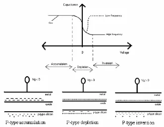
inversion, as seen in the following Figures for a p-type substrate. Figure 3.2 shows the
distribution of charge in the P-type MOS structure and how it should correlate to an ideal
C-V curve. In order to understand how accumulation, depletion and inversion are related
to the C-V curve, it is helpful to qualitatively look at each separately.
[image:27.612.141.472.429.686.2]During accumulation, the DC bias causes majority carriers (holes for the p-type
substrate) to pileup at the interface of the dielectric. For most semiconductor doping
levels, majority carriers will respond quickly enough to slightly add or subtract charge
from the two sides of the oxide at AC measurement frequencies up to 1 MHz. Since this
relatively small amount of charge is added or subtracted close to the edges of the
insulator, the charge configuration basically equivalent to an ordinary parallel-plate
capacitor. Whether a low or high probing frequency is used, the capacitance is equal to
the oxide capacitance as seen in Equation 3.3:
ox x o o ox acc x A k C
C = =ε [16] (3.3)
Where eo is the permittivity of free space, kox is the dielectric constant, A is the area of
the capacitor, and xox is the thickness of the dielectric.
Under depletion, a DC bias repels majority carriers from the oxide/silicon interface.
This results in an effective width from the interface being depleted of majority carriers.
The depletion width, W, fluctuates with AC bias as well as varies directly with the DC
bias. Because the depletion width is dependent on bias, the capacitance of the
semiconductor changes as seen in equation 3.4:
W A k C s o
s
ε
= [16]
(3.4)
As a result of the fact that the semiconductor capacitance is in series with the oxide
capacitance, the effective capacitance during depletion is that of Equation 3.5.
where Cs is the semiconductor capacitance, W is the width of the depletion layer and ks is
the dielectric constant of the semiconductor.
The behavior associated with depletion comes to an end upon inversion. At this
point, minority carriers begin to pileup at the oxide/semiconductor interface in response
to the DC bias. Unlike accumulation and depletion, inversion is affected by AC probe
frequency. Inversion C-V characteristics, therefore, act differently for low and high AC
probe frequencies.
For a low probe frequency, minority carriers have enough time to be generated or
annihilated along with the AC signal. This essentially results in the AC states behaving
like a succession of DC states where charge is being added or subtracted close to the
edges of the dielectric. For this situation, the capacitance approaches Cox, just as it did in
accumulation.
For a high probe frequency, minority carriers are unable to be supplied or eliminated
in response to the AC signal. The number of minority carriers at the inversion layer then
becomes fixed and the depletion width just fluctuates about a maximized depletion width
Wdm. This width is represented by Equation 3.6.
a i a si dm N q n N kT
W = 4ε ln(2 / ) [17] (3.6)
With W forming a maximum of Wdm, and an inadequate time for generation of
minority carriers, the inversion capacitance for a high frequency measurement is as
Accumulation, depletion and inversion of an N-type semiconductor is
qualitatively the same, except the majority carrier is the electron, and the C-V curve is
mirrored about the C-axis [18].
3.3 Interface Trap Density Distributions
There are many methods to extract interface trap density by using C-V measurements.
One of the most accurate techniques is referred to as the Kuhn method. To extract Dit by
this method, the semiconductor capacitance Cs is correlated to the low frequency
capacitance Clf with the following equation:
) ( 1 S LF OX LF OX it C C C C C q D − − = [16] (3.8)
The semiconductor capacitance is CS is determined by Equation 3.9:
(3.9) ] 1 ) )[exp( exp( ] 1 ) )[exp( exp( ) 1 ( ) 1 ( 2 , − − − + − + − − + − = − − ∧ S S F S S F U U U U D o s S LF S U U U U U U e e e e L K C S F S F
U
ε Where: kT q potential surface normalized U S S φ = = _ _ kT q potential Fermi normalized U F F φ = = _ _ i o S D n q kT K length Debye rinsic L 2 2 _ _int = ε
= S S U U potential surface of sign S
U
= _ _ _ =| |As seen in equation 3.9, Cs is dependent on surface potential, but CLF is a function of
gate bias. In order to solve for the interface trap density, as seen in equation 3.8, a
relationship must correlate surface potential to gate bias. This relationship is as follows:
=
∫
− G+∆V
V OX
LF
S dV
C C
G
G
) 1
( 2
1
φ [16]
(3.10)
where ? is an integration constant given by the surface potential at VG=VG1.
Choosing VG1 and VG2 such that the integration is carried out from accumulation to
strong inversion solves the integral above. The Kuhn method fits experimental and
theoretical CLF versus surface potential. The lateral voltage shift between the
experimental and theoretical curves is equal to the integration constant relating surface
potential to gate voltage. With CLF, CS, and the integration constant correlating VG to
FS, Dit can be determined over the entire band gap using equation 3.8. A typical
interface trap density distribution can be seen below in Figure 3.3 [16].
Interface Trap Density Distribution
1.00E+10 1.00E+11 1.00E+12 1.00E+13 1.00E+14 1.00E+15
0.30 0.50 0.70 0.90
E-eV (eV)
Dit (States/cm^2/eV)
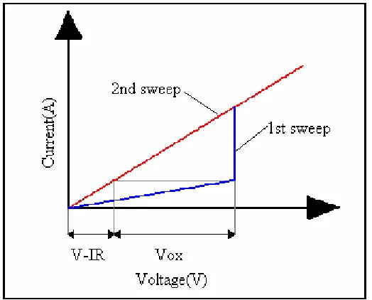
3.4 Breakdown and Leakage Measurements
Current-Voltage measurements can be used to determine breakdown fields and
leakage currents of oxides. The oxide in a MOS capacitor physically breaks down when
a high enough voltage is applied across it. To measure the breakdown field, Voltage is
plotted against current as shown in Figure 3.4.
Figure 3.4: I-V breakdown measurement
The capacitor is wired in series with a 1MO resistor and swept twice. The first sweep
physically breaks down the oxide, while the second sweep provides an I-V curve
corresponding (very closely) to the resistor in series. The current measured at the point
of breakdown is matched with a current on the second sweep. The voltage at which these
currents meet corresponds to the potential drop across the wafer. From this the voltage
drop across the oxide is deduced. To determine the breakdown field, the voltage drop
across the oxide is divided by the oxide thickness. By using this method, leakage
[image:32.612.194.456.228.439.2]3.5
Mobile Charge Measurements
There are two C-V tests that can be used to measure mobile ion content in a dielectric
film. The first is a temperature bias stress test. After an initial C-V curve is taken, the
wafer is heated to an elevated temperature (250°C-300°C) and a voltage stress is induced
for a short period of time (~5-10 min.). When a negative stress is applied, positive
mobile ions move to the surface of the dielectric in contact with the metal effectively
increasing Vfb and shifting the C-V curve to the right. When a positive stress is applied,
mobile ions move down to the silicon interface decreasing Vfb and shifting the C-V curve
to the left. After the wafer is stressed at a high temperature, it is cooled down and the
C-V measurement is taken. This is done twice, once with a positive stress and once with
a negative stress. The voltage shift between the two C-V curves (that were oppositely
stressed) corresponds to the mobile ionic charge according to the following equation: [6]
) (
) ( )
(/ 2
ox ox o M
t q V cm
N =∆ ε ε [6] (3.11)
The second method of measuring mobile charge in a dielectric film is the triangular
voltage sweep (TVS) method. For this experiment, a negative stress is applied at a high
temperature to attract all of the mobile ions to the top of the dielectric. A high
temperature, low frequency C-V curve is then done sweeping from positive to negative
voltages. Mobile ions then travel from the top of the dielectric film down to the interface
with the silicon as the bias changes from positive to negative. This ion current results in
a peak in the measured capacitance. The area under the peak is then related to the mobile
ion content by equation 3.12.
RqA dV V I
In Equation 3.12, the integral in the numerator is equal to the area under the capacitance
peak, R is equal to the sweep rate (V/s), q is the charge of an electron and A is the area of
the capacitor (cm2).
The TVS measurement is also able to determine if there are more than one mobile
ionic species within a dielectric. When this is the case, there will be two separate
capacitance peaks. This occurs when there is a difference in mass. Atoms with a lower
diffusivities move slower, so they form broader peaks that are on the left. Ions with
higher diffusivities move faster and form a narrower capacitance peak.
3.6 Current-Voltage for Transistor Parameters
A transistor has two modes of operation, linear and saturation. Their biasing
conditions are shown for an n-channel MOSFET in the following relationships below.
Linear operation [19]
Saturation operation [19]
In the linear regime, the inversion layer extends all the way from the source to the
drain. The drain current is also a function of the drain voltage such that higher drain
biases result in increased drain current. In saturation mode, the drain bias is high enough
to pinch off the inversion channel near the drain. Electrons in the channel region are
pulled through the pinched off region at the saturation drift velocity as a result of the high
longitudinal electric field. This allows for the drain current to be maximized and no
longer a strong function of drain bias [19]. When testing transistors, they are typically
tested using I-V curves in both linear and saturation regimes.
) (VG Vt D
V t V g V
− > >
) (VG Vt D
V t V g V
CHAPTER 4
PLASMA-INDUCED CHARGE DAMAGE
4.1 Introduction
Plasma is needed in MOSFET processing for many fabrication steps such as
sputtering, etching, photoresist ashing, and dielectric deposition. In certain cases, it
allows for decreased processing temperatures. Exposure to plasma may result in damage
from unwanted chemical reactions, electron-hole pair creation, and oxide charging. Of
these, the most significant source of damage to the modern sub-quarter micron transistor
is gate oxide charging [20]. The gate oxide has a specific vulnerability to such
processing steps because it is fragile and must tolerate high applied electric fields, both
during processing and in device operation.
When exposed directly to plasma, a high electric field can be dropped across the gate
oxide. Gate oxide degradation occurs when the field across it is high enough to produce
Fowler-Nordheim (F-N) tunneling current from the bulk silicon to the gate [20]. This
mechanism is responsible for breaking bonds at the silicon/SiO2 interface, as well as
resulting in an increased bulk oxide charge [20, 21]. It generally results in decreased
lifetime and reliability of devices [20]. In some cases the field is high enough to result in
a physical breakdown of the oxide, causing reduced yield.
Figure 4.1 shows band diagrams for the MOS structure at equilibrium (Vg=0) and at
high field conditions. In part (A) the only way for an electron to get from the silicon to
the gate metal is to directly tunnel through the entire energy barrier of the oxide, which is
especially for thicker oxides. Part (B) of Figure 4.1 shows the same band structure of the
MOS device under a high electric field; a situation where the gate metal has a positive
bias. With a high electric field the energy bands bend more abruptly, decreasing the
thickness of the tunneling barrier and increasing the probability of a carrier tunneling.
Tunneling under these conditions is referred to as F-N tunneling. This mechanism of
current flow is responsible for the damage induced by high- field processing, as in most
plasma processes. It is also worth noting that under typical bias conditions inversion may
occur for p-type (boron-doped) silicon, allowing minority electron carriers to tunnel into
the gate oxide. This can be seen in Figure 4.1 (B) where the Fermi level (EF) is crossed
by the intrinsic energy level (Ei), resulting in charge inversion at the surface.
The degree of gate oxide degradation is directly related to the field- induced F-N
[image:36.612.121.512.77.322.2]conducting surfaces connected to the gate. Metals connecting to the gate act as antennae
structures that collect charge during plasma processing. The ability of these structures to
collect charge is directly related to the gate oxide E- field experienced, and the resulting
degree of damage to the dielectric layer. This quantity of charge is usually referred to as
the antenna ratio. The antenna ratio is defined as the ratio of the area of conducting
material over the thick oxide (that is connected to the gate) to the area of the gate. As this
quantity increases, the extent of the damage done to the gate oxide will increase
accordingly [20].
4.2 Electron and Hole Trap Generation
Charge trap centers in the bulk of an oxide are considered to be amphoteric meaning
that they can become both negatively and positively charged. Trapped charge residing in
the bulk of the gate oxide originates from weak Si-Si bonds where there is an oxygen
vacancy between them; each silicon atom is back-bonded with three oxygen atoms (see
Figure 4.2). The most common and widely accepted model to represent both electron and
hole trapping is known as the HDL model (Harry Diamond Laboratories) [22, 23]. The
HDL model suggests that the Si-Si bond is broken by free holes produced by radiation.
This radiation could be from sources such as x-ray lithography [23], or plasma
photo-generation [24]. The breaking of weak Si-Si bonds results in the formation of positive
charge centers (filled hole-traps). These positive charge centers can remain charged, or
combine with electron(s) and change their charge state [22]. A diagram of the HDL
Figure 4.2: HDP model for hole & electron trapping [22]
Part (A) of Figure 4.2 shows the precursor of the charge trap before it is broken by the
radiation- induced hole. As the hole breaks the Si-Si bond, it becomes trapped to one of
the silicon atoms and moves away from the uncharged silicon atom. The hole-trap then
takes on a relaxed configuration where the oxygen atoms become planar. At this point
the trapped hole can be forward annealed by the application of a positive field across the
oxide resulting in electrons from the substrate neutralizing the charge. A neutral dipole
results upon capture of one electron [22]. From here, it can be reverse annealed, by
applying a negative field across the oxide forcing the electron back toward the bulk. This
returns the charge center back to the trapped hole seen in part (B) of the figure. If this
doesn’t happen, the neutral dipole acts as an electron trap and traps a second electron to
neutral silicon atom by what is referred to as true annealing. A similar representation of
this phenomenon can be seen in Figure 4.3.
Figure 4.3: Electron and hole trap generation and annihilation processes [22]
4.3 Oxide Traps and Gate Leakage
Under rigorous operating conditions, elevated temperature and high- field conditions
can cause the gate oxide integrity to degrade over time until it experiences catastrophic
failure, known as breakdown. Common methods of determining resistance to failure are
electric field breakdown (Ebd) tests, gate leakage measurements (below the E- field at
which F-N or direct tunneling becomes significant) and charge to breakdown
measurements (Qbd). A desirable dielectric will have a high breakdown field, low gate
leakage current and a high charge to breakdown value, which correspond to long device
lifetimes.
Broken bonds and structural rearrangement associated with oxide traps can lead to
higher leakage currents, as well as lower Ebd and Qbd measurements. This has been
of a high field. The increase in leakage current is attributed to tunneling via
stress-generated positive charge centers, local decreases in the tunneling barrier at defect sites,
and trap assisted tunneling. The number of oxide traps generated by a high E- field has
been shown to be proportional to the increase in leakage current [25].
When oxide traps are located in the bulk of an oxide, there are extra energy levels
between the valence and conduction bands of SiO2. With no trap states, an electron must
obtain ~3eV in order to surmount the energy barrier between silicon and SiO2 and
contribute to current flow; the hole energy barrier is ~ 4eV [18]. Oxide traps present
available energy states within the energy barrier that can act as stepping-stones for
carriers to reach the conduction band. This makes it easier for charge to penetrate the
oxide and assists in providing increased leakage current [18]. Note that a poor quality
oxide layer may allow conduction through defect states without carriers surmounting or
tunneling through the energy barrier.
4.4 Assessment of Plasma Induced Charge Damage
Both fully processed transistors and MOS capacitors can be used to assess plasma
damage to thin oxides. Capacitors are preferred because of their short process time and
ability to utilize wet processing for control samples in order to isolate the influence of
particular plasma processes. Capacitance-Voltage (C-V) characteristics can be
specifically used to determine interface trap densities by means of quasi-static
measurements and the observed stretching in high frequency characteristics due to
interface states. This allows a direct correlation between the creation of interface traps to
hard to capture using only capacitors. C-V data also may not provide adequate
information regarding oxide charge trapping, as practical limitations on antenna ratios
will not be consistent with values for actual transistors. For a more complete assessment
of actual damage, it is usually necessary to fabricate transistors [20].
If transistors are fabricated, direct measurements of threshold voltage, gate leakage,
sub-threshold swing, and transconductance can be made to characterize the influence of
plasma damage. Bulk oxide trapping will result in increased threshold voltages and gate
leakage while interfacial damage results in increased sub-threshold swings and decreased
transconductance. Disadvantages of fully processed transistors to assess plasma damage
include inability to accurately pinpoint critical process steps as well and difficulty in
producing a reference with no plasma exposure [20].
For devices fabrication in this study, there are many process opportunities for the
introduction of plasma induced damage. To isolate the influence of specific plasma
processes and to avoid factor confounding, alternatives to plasma processes were used in
certain situations (e.g. solvent photoresist strip instead of oxygen plasma ash). Processes
where plasma induced damage are of primary concern include the metal gate sputter
deposition, the gate reactive- ion etch (RIE), the inter- level dielectric deposition (ILD),
and the contact/interconnect aluminum sputter deposition. The next chapter will describe
CHAPTER 5
EXPERIMENTAL DESIGN & DEVICE FABRICATION
5.1 Capacitor Experimental Design
An LPCVD oxide is the current gate dielectric for low temperature CMOS processing
at RIT. It was initially chosen over a PECVD oxide because it showed lower and more
uniform interface trap densities. For large-scale manufacturing, a PECVD oxide is far
more practical as it results in a more uniform film and much faster deposition rates. For
this work, PECVD and LPCVD oxide films were both chosen for a study on the effects
of remaining process-induced damage, following low and high temperature annealing.
An anneal temperature of 600°C was implemented for the low-temperature process
constraint, as this temperature represents an upper limit of most thin- film transistor (TFT)
fabrication on glass substrate material. Annealing at higher temperatures (up to 900°C)
was also investigated to determine the thermal stability of the oxide damage. Capacitors
were fabricated using these annealing conditions to compare the dielectric characteristics
of the oxide films.
5.2 Capacitor Fabrication
All wafers were given a standard RCA Clean to remove contaminants and native
oxides and provide a pristine surface for film deposition. Table 5.1 shows the initial
SiO2 Material Anneal Temp
(N2 Ambient, 2hr)
LPCVD LTO 600°C
LPCVD LTO 900°C
PECVD TEOS 600°C
PECVD TEOS 900°C
Thermal SiO2 None
Table 5.1: Capacitor treatment combinations
Aluminum was evaporated, followed by capacitor gate patterning using a GCA g- line 5X
reduction stepper. The aluminum was etched using Transene type-A aluminum etchant,
followed by a solvent photoresist removal. Wafers were finally sintered in H2/N2 at
450°C for 30 minutes. Cross-sections of the process are shown in Figure 5.1.
Figure 5.1: Cross-section of capacitor fabrication Oxide Deposition
Resist Pattern
Al Etch
5.3 Transistor Experimental Design
An experiment was designed to investigate the effect of plasma charging from the
ILD deposition on metal- gate NMOS transistors. The standard low-temperature NMOS
process utilized a 500? LTO gate oxide with a self-aligned molybdenum gate [26]. The
devices were fabricated using the same oxide films as the capacitors identified in Table
5.1. Both the standard PECVD TEOS ILD recipe and a low power recipe were
investigated. It was initially expected that when reducing the power for the ILD
deposition, plasma damage would be less pronounced. This was based on the assumption
that a lower power consisted of decreased voltage (not just current) resulting in a
decreased field drop across the gate oxide during processing. Previous data suggests that
the treatment combination with an LTO gate oxide and TEOS ILD annealed at 600°C
exhibits significant charge damage [26]. Different annealing temperatures were
implemented to determine the annealing conditions required to remove the damage.
Table 5.2 shows the design space for the experiment. An LTO ILD was used as a
reference (control) to isolate any observed differences to the PECVD TEOS ILD
deposition (see last three treatment combinations in Table 5.2).
The screen oxide shown in Table 5.2 was a 500? film to protect the molybdenum
gate during thermal processes and serve as a screen oxide for the source/drain implants.
The standard PECVD oxide process was used for this thin screen oxide (with the
exception of the last three treatment combinations) because process results indicated
superior protection compared to the LTO film [26]. The PECVD screen oxide deposition
to the gate oxide, the process was cons istent over the treatment combinations explored.
Each treatment combination was done on a separate wafer.
Gate oxide
Screen
oxide ILD
Anneal Temperature
(degrees C)
LTO TEOS TEOS 600
LTO TEOS TEOS 700
LTO TEOS TEOS 800
LTO TEOS TEOS 900
LTO TEOS LP TEOS 600
LTO TEOS LP TEOS 900
Thermal TEOS TEOS 600
Thermal TEOS TEOS 900
Thermal TEOS LP TEOS 600
Thermal TEOS LP TEOS 900
TEOS TEOS TEOS 600
TEOS TEOS TEOS 900
TEOS TEOS LP TEOS 600
TEOS TEOS LP TEOS 900
TEOS LTO LTO 600
LTO LTO LTO 600
[image:45.612.182.431.176.513.2]Thermal LTO LTO 600
Table 5.2: Designed-experiment treatment Combinations
5.4 Transistor Fabrication
Transistors were fabricated using a CMOS process and mask set developed by Robert
Manley and Robert Saxer [26]. Slight changes were made to simplify processes and only
Step 1: RCA clean
A standard RCA clean [27] was first done in order to remove any initial
contamination prior to processing. The clean process is shown in Table 5.2 shows the
makeup of different chemical baths used. The APM bath is used to remove organic
contamination while the HPM bath helps remove metallic contamination. HF is used in
the process to remove any native oxide that may be on the silicon surface. Wafers were
then dried in a spin-rinse-dry (SRD) machine.
Step 2: Well Implant
The well implant was done using the B11 species of boron at an energy of 170KeV and a
dose of 1.2x10¹³ ions/cm2. This dose was high enough to eliminate the need for a
channel stop implant.
Step 3: Well Drive
A 500? pad oxide was grown and the well implant was driven in at 1000°C for 25 hours
in nitrogen ambient. This was done to diffuse and activate well dopant into the silicon
lattice. A cross-section of the device at this point is shown in Figure 5.2.
Figure 5.2: Cross-section of P-well and pad oxide formation
P+ implant
Step 4: Backside Implant
The backs of the wafers were implanted with B11 at an energy of 35KeV and a dose
of 2x10¹⁵ ions/cm2. This was done to provide a more ohmic back contact in order for the
bulk silicon to be adequately grounded during testing.
Figure 5.3: Back side contact implant
Step 5: LPCVD Field Oxide Deposition
A 4000? field oxide was deposited using LPCVD in order to create isolation between
devices. A SiH4 flow of 50sccm and an O2 flow of 120sccm were used for a deposition
time of 28.5 minutes. A cross-section of this step is shown in Figure 5.4.
Figure 5.4: Field oxide deposition
P+ implant
Si-Substrate Oxide
P+ implant
Step 6: Backside Anneal
A high temperature anneal was done at 900°C in nitrogen for 10 minutes in order to
activate the dopant from the backside implant. The anneal was also used to densify the
field oxide.
Step 7: Active Lithography
Resist was patterned on top of the field oxide to define the active region. Rohm and
Haas 1813 Resist was coated using an SVG wafer track on program 1. (See Appendix
for details)
The wafers were exposed on a GCA g- line stepper for 0.64s using the EAGLEPLG
program with pass 3. This pass exposes every die on the wafer except for 4. These were
left to make embedded capacitors on each wafer. On this lithography step, pass 1 was
used through a clear mask in order to open up the areas in the field oxide where
capacitors were to be made. The wafers where then developed using recipe number 1 on
the SVG track. (See Appendix for process details)
Figure 5.5 shows the cross-section of the devices after resist was coated, exposed and
developed. The opening in the left of the Figure defines the active region for a transistor
Figure 5.5: Active lithography
Step 8: Active Etch
The active etch was done in Buffered Oxide Etch (BOE) made up of 10 parts
ammonium fluoride and 1 part HF. Wafers were etched in the BOE for 10 minutes,
which corresponded to a 20% over-etch.
Step 9: Resist Strip
Resist was stripped using solvent strip at 70°C for 20 minutes. Wet resist removal
was used for the entire experiment to rule out plasma charging from the photo-resist
asher. After the resist strip, it was rinsed in DI water for 5 minutes and put through a
spin-rinse-dry. The cross-section in Figure 5.6 shows the wafer processed up to this
point.
P+ implant
[image:49.612.110.518.73.277.2]Figure 5.6: Active etch and resist strip
Step 10: Scribe wafers
Wafers were scribed in order to identify each treatment combination. They were
purposefully scribed at this point rather than the beginning of the process. This was to
ensure that defects from the scribe did not propagate through the wafer during the 25
hour anneal.
Step 11: RCA clean
The same RCA clean described in step 1 was used to ensure that the surface was pristine
for the gate dielectric deposition.
Step 12: Gate Oxide Deposition
A target thickness of 500? of LPCVD oxide was deposited at 425°C with a SiH4 gas
flow of 50sccm and an O2 gas flow of 120sccm. The deposition time was 2.73 minutes.
P+ implant
[image:50.612.113.524.73.276.2]For the PECVD oxide, the PECVD TEOS deposit ion was conducted using an
Applied Materials P5000. For 500? of PECVD oxide, conditions were a TEOS flow of
400sccm, an O2 flow of 285sccm, a pressure of 9Torr, power of 205W, and a gap spacing
of 220 mils. The deposition time was 4.4 seconds.
For 500? of thermal oxide, a BRUCE furnace was used. The oxidation temperature
was 100°C and the O2 gas flow was 10 lpm. The oxidation time was 42.5 minutes.
Figure 5.7 shows the transistor cross-sections corresponding to the deposition of the gate
oxide.
Figure 5.7: Gate oxide deposition
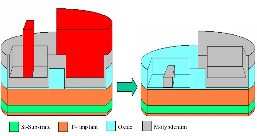
Step 13: Molybdenum Gate Deposition
Because of its high melting point, molybdenum was used rather than aluminum for
the self aligned gate structure. It was sputtered with an RF sputtering tool with 15sccm
of Ar. Base pressure was 7.5e-7Torr, deposition pressure was 14mTorr, forward power
was 1000W, and reflected power was 0W. For the 5000? thick gate, the deposition time
was 53 minutes. The cross-section is shown in Figure 5.8.
P+ implant
Figure 5.8: Molybdenum gate deposition
Step 14: Gate Lithography
Resist was coated with recipe 1 and developed with recipe 1 on an SVG wafer track
as described in step 7. The EAGLEPLG program was used with pass 3 and the exposure
time was 0.7s. This resulted in only exposing transistor die. The cross-section of this is
shown in Figure 5.9.
Figure 5.9: Gate lithography
P+ implant
Si-Substrate Oxide Molybdenum
P+ implant
[image:52.612.109.525.457.686.2]Step 15: Gate Etch
The gate etch was done in a Drytec Quad reactive ion etcher. It was done with a
power of 250W, a pressure of 150mTorr, and an SF6 gas flow of 50sccm. The etch time
was approximately 1.8 minutes.
Step 16: Resist Strip
Resist was stripped off using solvent strip as described in step 9. The cross-section of
the device up to this point is shown in Figure 5.10.
Figure 5.10: Cross-section after gate etch and resist strip.
Step 17: Screen oxide deposition
A 500? oxide was deposited over the molybdenum gate to protect it from oxidizing.
It also served as the screen oxide for the source/drain implants. It was deposited with a
power of 205W, a TEOS flow of 400sccm, an O2 flow of 285sccm, a pressure of 9Torr,
P+ imp lant
[image:53.612.110.540.301.528.2]and a gap spacing of 220mils. Control wafers received an LPCVD screen oxide
deposited just as the gate oxide was. The cross-sections are shown in Figure 5.11.
Figure 5.11: Cross-section of screen oxide deposition
Step 18: Source/Drain Implant
Source drain implants were done using a Varion 350D ion implanter. P31 species of
phosphorous was implanted with a dose 4x10¹⁵ ions/cm2, and an energy of 110KeV. A
cross-section of the device after the source/drain implant is shown in Figure 5.12.
Figure 5.12: Cross-section of source drain implants
P+ implant
Si-Substrate Oxide Molybdenum
Step 19: Inter-Level Dielectric Deposition
For half of the experimental wafers, the standard TEOS ILD was deposited. This
used the same parameters described in step 17. The deposition time was increased to
29.8s to obtain a thickness of 4000?. The other half of the wafers received a TEOS ILD
deposited at a significantly lower power. A power of 50W was used instead of the
standard 205W. Pressure was also decreased to 2.5Torr, TEOS flow was reduced to
100sccm, O2 flow was reduced to 71sccm, and the gap spacing was adjusted to 215mils.
The adjustments for this recipe were originally made by Germain Fenger to minimize
stress in the ILD film. The three control wafers received an LPCVD deposition with the
same gas flows and temperature as described in step 12. Deposition time was increased
to 28.3 minutes to obtain a 4000? oxide. A cross-section of the ILD deposition is shown
in Figure 5.13.
Figure 5.13: ILD deposition
![Figure 4.1: Direct band-to-band tunneling & Fowler-Nordheim tunneling [18]](https://thumb-us.123doks.com/thumbv2/123dok_us/120479.11593/36.612.121.512.77.322/figure-direct-band-band-tunneling-fowler-nordheim-tunneling.webp)
![Figure 4.2: HDP model for hole & electron trapping [22]](https://thumb-us.123doks.com/thumbv2/123dok_us/120479.11593/38.612.112.522.70.373/figure-hdp-model-hole-electron-trapping.webp)