DEVELOPMENT OF FAULT DETECTION SYSTEM FOR THREE--PHASE VOLTAGE SOURCE INVERTER (VSI)
Sa’adah Binti Daud
ii
“I hereby declare that I have read through this report entitle “Development of Fault Detection
System for Three-phase Voltage Source Inverter (VSI)” and found that it has comply the
partial fulfillment for awarding the degree of Bachelor of Electrical Engineering (Industrial
Power)”
Signature : ……….
Supervisor’s Name : DR. ABDUL RAHIM BIN ABDULLAH
ii
DEVELOPMENT OF FAULT DETECTION SYSTEM IN THREE-PHASE VOLTAGE SOURCE INVERTER (VSI)
SA’ADAH BINTI DAUD
A report submitted in partial fulfillment of the requirements for the degree of Bachelor of Electrical Engineering (Industrial Power)
Faculty of Electrical Engineering
UNIVERSITI TEKNIKAL MALAYSIA MELAKA
iii
I declare that this report entitle “Development of Fault Detection System for Three-phase Voltage Source Inverter (VSI)” is the result of my own research except as cited in the
references. The report has not been accepted for any degree and is not concurrently submitted
in candidature of any other degree.
Signature : ……….
Name : SA’ADAH BINTI DAUD
iv
v
ACKNOWLEDGEMENT
I am Sa’adah Binti Daud would like to express the gratitude to Allah for His
guidance throughout the process of finishing this report while undergoing this
project. Alhamdulillah, this progress report has been completed with success and full
of inspiration. I would like to offer thanks to my parents who gave their full moral
support and encouragement that I managed to complete this report. Besides that, a lot
of thanks to my supervisor Dr. Abdul Rahim bin Abdullah who is willingly to guide
me and teach me a lot in order to give better understanding and to accomplish my
project. Lots of thanks to all friends for the guidance, cooperative and compromise
vi
ABSTRACT
Voltage Source Inverter (VSI) is widely used in larger electronics areas, portable
devices and in power generation systems. Lately, this device is highly demand in applications
using renewable energy such as Solar Photovoltaic (PV) System and Smart Grid System. As
time move on, the development of technologies using renewable energy is needed for future
demand since this resource helps in protecting the surrounding. In industry, the performance
and effects of the devices are such important factors that must be taken into account in order to
ensure the continuity of the applications. Normally, the faults occur on the switching device
that is very sensitive. A small electric disturbance may cause destruction at high cost and
sudden system failure. The development of fault detection system for Voltage Source Inverter
(VSI) is to monitor and detect fault at the early stage. This fault can be detected by the
behavior of current waveform. This project aims are to analyze the system based on RMS and
average current as the parameters, to develop the system with accurate value measurement and
to classify the types of fault occurs. Analysis is conducted in order to identify the fault pattern
or behavior by using MATLAB. This analysis will first undergo the circuit design process
using Simulink, a tool in MATLAB. The simulation will result in the classification of faults’
type. The project designed is focused on applications using three-phase VSI. This system is
design using Microsoft Visual Basic 2010 and is known as “VSI Fault Detection System” that
can detect and classify only two types of fault which are short-circuit fault and open-circuit
fault. The use of NI USB-6009 DAQ Card is to capture signal source or data and interface it
with Visual Basic 10.0. The monitor can display the parameters reading and waveform which
are RMS current and average current. The type of fault is mention in the system once fault is
detected. This system provides precaution and early identification of fault thus reduces high
vii
ABSTRAK
Voltan sumber inverter (VSI) digunakan secara meluas dalam sistem penjanaan kuasa,
bidang elektronik dan digunakan untuk peranti mudah alih. Penggunaan peranti ini mendapat
permintaan yang luas dalam aplikasi yang menggunakan sumber tenaga yang boleh
diperbaharui seperti Sistem Solar Photovoltaic (PV) dan sistem Grid Pintar. Justeru itu,
penggunaan sumber yang boleh diperbaharui sangat berguna dalam memenuhi keperluan masa
depan disamping dapat melindungi alam sekitar. Keberkesanan dan prestasi sesebuah peranti
merupakan salah satu faktor penting untuk memastikan kelancaran sesuatu aplikasi atau
sistem. Kebiasaannya, kerosakan berlaku pada suis di dalam litar VSI. Suis-suis yang terdedah
kepada gangguan kecil elektrik boleh menyebabkan peranti rosak serta kegagalan sistem
beroperasi secara tiba-tiba. Penghasilan sistem pengesan gangguan untuk Voltan sumber
inverter (VSI) boleh mengesan dan memantau kerosakan pada peringkat awal. Kerosakan ini
dapat dikesan melaui bentuk dan corak gelombang arus. Tujuan projek ini adalah untuk
menganalisis sistem berdasarkan arus RMS dan arus purata, untuk menghasilkan sistem yang
dapat beroperasi dengan tepat dan untuk mengenalpasti jenis kerosakan yang berlaku. Analisis
dijalankan untuk mengenal pasti corak gangguan dengan menggunakan MATLAB. Reka
bentuk litar dihasilkan dengan menggunakan Simulink dan jenis kerosakan atau kesalahan
dapat dikesan dan dikategorikan melalui proses simulasi. Projek ini direka untuk aplikasi
three-phase VSI. Sistem ini dihasilkan menggunakan Microsoft Visual Basic 2010 dan dikenali sebagai “VSI Fault Detection System” yang boleh mengesan dan mengelaskan dua
jenis kerosakan sahaja iaitu litar pintas atau litar terbuka. NI USB-6009 digunakan sebagai
perantara yang dapat merakam isyarat signal dan menterjemahkannya kepada bahasa yang
difahami oleh Visual Basic 10. Monitor memaparkan bacaan parameter dan corak gelombang
iaitu arus RMS (RMS current) dan arus purata (average current). Jenis-jenis kerosakan VSI
akan dipaparkan apabila sistem mengesannya. Sistem ini dapat mengurangkan kos
viii
TABLE OF CONTENT
CHAPTER TITLE PAGE
ACKNOWLEDGEMENT v
ABSTRACT vi
ABSTRAK vii
LIST OF TABLES xi
LIST OF FIGURES xii
1 INTRODUCTION 1
1.1 Research Background 1
1.2 Problem Statements 4
1.3 Project’s Objectives 4
1.4 Project’s Scopes 5
2 LITERATURE REVIEW 6
2.1 Theory and Basic Principles 6
2.1.1 Voltage Source Inverter (VSI) 6
2.1.2 Fault Detection in VSI 9
2.1.3 Visual Basic 10
ix
CHAPTER TITLE PAGE
2.1.5 NI USB-6009 DAQ Card 12
2.2 Review of Previous Related Works 13
2.3 Summary of the Review 15
2.4 Discussion on Chosen Technique 17
3 RESEARCH METHODOLOGY 22
3.1 Proposed System 22
3.2 Flowchart of Research Methodology 23
3.2.1 Literature Review 24
3.2.2 Simulation Using MATLAB Simulink 25
3.2.3 Implementation of Microsoft Visual Basic 2010
Software. 26
3.2.4 Hardware Implementation 29
3.2.5 Combination of Hardware and Software 32
3.2.6 Testing and Troubleshooting 32
3.2 Project Milestone 33
4 RESULTS AND DISCUSSION 34
4.1 Results 34
4.1.1 Simulation using MATLAB Simulink 34
4.1.2 Fault Detection using Analysis 39
4.1.3 Graphical User Interface (GUI) Design in Visual
Basic2010 44
4.1.4 Hardware Design 48
x
CHAPTER TITLE PAGE
4.2 Project achievements 53
5 CONCLUSIONS 56
REFERENCES 58
xi
LIST OF TABLES
TABLE TITLE PAGE
2.1 Switching scheme of three-phase inverter 8
2.2 Summary of the review 16
3.1 Pin descriptions 30
3.2 Project milestone 33
4.1 Analysis of fault occurs at Phase A 44
xii
LIST OF FIGURES
FIGURE TITLE PAGE
1.1 Illustration of voltage source inverter 2
1.2 A grid-connected solar PV system 2
1.3 A HVDC power transmission 3
2.1 Half-bridge Single-phase VSI 7
2.2 Single-phase Full-bridge VSI 7
2.3 Three-phase VSI 8
2.4 Waveform of the switching sequence of three-phase VSI 9
2.5 USB-6009 DAQ Card 12
2.6 VSI three-phase ac drive structure 18
2.7 An Ideal gating signal 19
2.8 Open circuit fault 19
2.9 Short circuit fault 20
3.1 Illustration of the project 22
3.2 Block diagram of the project 23
3.3 Flowchart of research methodology 23
3.4 Model of VSI switches 25
3.5 Advantages of Visual Basic 27
3.6 Visual Basic 2010 logo 28
xiii
FIGURES TITLE PAGE
3.8 NI USB-6009 pinout 29
3.9 SCT013, 100A:50mA Current Sensor 31
3.10 SCT013, 100A:50mA schematic diagram 32
3.11 Inverter circuit connection 33
4.1 Designed circuit using Simulink 34
4.2 Three-phase VSI waveform during Normal Condition 35
4.3 Upper and lower switch short circuit fault signal Phase A 36
4.4 Waveform pattern when short circuits at lower switch Phase
A
36
4.5 Waveform pattern when short circuits at upper switch Phase
A
37
4.6 Upper and lower switch open circuit fault signal Phase A 38
4.7 Waveform pattern when open circuits at upper switch Phase
A
38
4.8 Waveform pattern when open circuits at lower switch Phase
A
39
4.9 Average current when short circuit occurred at upper switch
of Phase A
40
4.10 RMS current when short circuit occurred at upper switch of
Phase A
40
4.11 Average current when short circuit occurred at lower switch
of Phase A
41
4.12 Current when short circuit occurred at lower switch of Phase
A
41
4.13 Average current when open circuit occurred at upper switch
of Phase A
42
4.14 RMS current when open circuit occurred at upper switch of
Phase A
xiv
FIGURES TITLE PAGE
4.15 Average current when open circuit occurred at lower switch
of Phase A
43
4.16 RMS current when open circuit occurred at lower switch of
Phase A
43
4.17 System designed using Visual Basic 2010 45
4.18 Button selection 45
4.19 The system when simulation runs 46
4.20 The file locations of data recorded 46
4.21 Data recorded in .txt format 47
4.22 Status box 47
4.23 Parameters value 48
4.24 Hardware connection diagram 48
4.25 System hardware 49
4.26 Connection for performance testing 49
4.27 Current waveform during no fault conditions 50
4.28 Open circuit fault waveform 50
4.29 Short circuit fault waveform 51
4.30 Current transducers clamped at each phase 51
4.31 The certificate of Silver Prize 53
4.32 The Siver Medal received during i-ENVEX 2014 54
4.33 The Outstanding Achievement Award during INNOFEST
2014
54
xv
LIST OF APPENDICES
APPENDIX TITLE PAGE
A Table A1 – Gant chart 58
B NI USB 6009 DAQ Card Datasheet 59
C SCT-013-000A, 100A:50mA Split Core current sensor
Datasheet 90
CHAPTER 1
INTRODUCTION
1.1 Research Background / Motivations
Recently, in industrial processes, automation has lead to comprehensive
electromechanical systems. The cost of production and operation are high, thus can cause a
rise in planned and unplanned standstill. Standstill or breakdown of a single of dozens of
drives usually leads to the complete malfunction of the system. Thus, a short standstill times
and high utilization over time are required for an economic operation. In case of inevitable
maintenance, only short interruption times are allowed and unplanned faults have to be kept
minimize [1]. Therefore, it is necessary to assure the safety and continuous operation for
application using this equipment since they can improve the productivity [2].
The most common drive in industry is inverters. Inverters are basically used to transfer
power from a DC source power to an AC load, such as an AC motor. In power electronics
context, the word “inverter” denotes a power conversion circuits that runs from a DC voltage
or current source and converts it into AC voltage or current as illustrated in Figure 1.1.
Examples of DC voltage source are battery bank, solar photovoltaic cells and an AC voltage
2
Figure 1.1: Illustration of voltage source inverter
These devices are widely used in power generation systems such as in solar generating
systems, electric utility companies that need the conversion of DC power source to AC loads,
in power grid and also in High Voltage Direct Current (HVDC) power transmission. They are
also widely used in larger electronics systems. Inverter circuits are being applied in industry
such as uninterruptable power supply (UPS) unit, electronic frequency charger, and adjustable
speed drives (ASD) for ac motors [3]. An example of application using inverters in a
grid-connected solar PV system is shown in Figure 1.2 while in HVDC power transmission is
shown in Figure 1.3.
[image:18.612.190.458.435.591.2]3
Figure 1.3: A HVDC power transmission. [5]
Apart from solar panels, inverters also play role in transmitting power from batteries
and fuel cells. Grid-tied inverters are used in solar electricity system. These inverters have the
ability to feed back energy into the utility grid since it produces alternating current with the
amplitude and frequency as the energy provided by the utility distribution network. Thus,
these help during blackout since they can be shut off. Therefore, inverters play a big role in
order to achieve or to make a system to be possibly operated. As time move on, the
development of technologies using renewable energy is needed for future generation to fulfill
their demand as well as to protect the environment and make it greener. So the inverters are
important device and their efficiency must be taken into account.
Inverters are divided into two types which are Current Source Inverter (CSI) and
Voltage Source Inverter (VSI). For Voltage Source Inverter (VSI), a DC voltage source is
converted to be fed to AC voltage load. Usually, the fault occurs at the switching device of the
circuit. There are several types of fault may appear in VSI namely DC link capacitor
short-circuit fault, Open-short-circuit fault, and short-short-circuit fault [6]. When these faults occur, the
associated system need to be stopped for a maintenance schedule. The main idea and
information about the waveform behavior of these faults are one of the important key for
protection and tolerant control for this equipment. This behavior must be analyzed in order to
detect the type of fault occuron the switching device.
This project presents the design and development of fault detection system to detect
and measure faults occur in Voltage Source Inverter (VSI) at the early stage. The system can
4
The parameter will be measured are current in RMS value and average value. The data will be
recorded and stored efficiently thus, the fault of VSI can be monitored.
1.2 Problem Statements
Most of power electronic devices such as Voltage Source Inverter (VSI) run in an
environment requiring rapid speed variation, frequent starting or stopping and constant
overloading. This circuit is subject to many failures such as constant abuse of voltage
overswings and the surge of over-current. Even though the devices come with protection such
as snubber circuits, switching devices are thermally fragile and physically small.
In Voltage Source Inverter (VSI), the faults normally occur on the switching device
that is very sensitive. Even a small electric disturbance can lead to the exceeding of thermal
rating resulting in rapid destruction. In case of expensive, high power systems, safety critical
system and multi-converter integrated automation systems, the presence of faults will result in
sudden system failure.
The occurrence of fault such as open-circuit fault and short-circuit fault will affect the
efficiency of a system or application. Prevention should be taken first to avoid much worst
damage. Thus, to prevent damages at a high cost, the fault occurrence must be monitored
earlier. The faults can be detected by the behavior of current waveform. Analysis must be
done to ease in identifying and classifying the types of fault occurs at the switches.
1.3 Objectives
The objectives of the proposed project are:
1. To analyze VSI fault detection system based on average current and RMS current
5
2. To develop VSI fault detection system that will provide accurate value for the
measurement parameters that is the average value and RMS value of current in
each phase of the system using Visual Basic 2010.
3. To classify types of fault occur in VSI whether it is open-circuit or short-circuit
faults.
1.4 Scopes
The scopes of this project are:
1. This project detects and classify fault in three-phase VSI whether it is open-circuit
fault or short-circuit fault.
2. This system utilizes the Microsoft Visual Basic 2010 software to display the
waveform behavior as well as measurement parameters and NI USB-6009 Data
Acquisition Card (DAQ card) to capture source signal and interface it with Visual
Basic 2010 software.
3. This project detects the occurrence of fault by the average and RMS current value.
4. The system designed display the RMS and average value of current.
CHAPTER 2
LITERATURE REVIEW
2.1 Theory and Basic Principles
2.1.1 Voltage Source Inverter (VSI)
Inverters are designed to provide either single-phase or three-phase output. Usually,
three-phase ac is required in larger industrial applications. Inverter is also classified into two
that is offline and online inverter. An inverter is called offline inverter or autonomous inverter
if it is the only source of the load ac line. If an inverter is a part of the common power supply
line, it is known as a line-fed inverter or online inverter. Voltage source inverter (VSI) and
current source inverter (CSI) are distinguished in accordance with the circuit arrangement
classification.
A Voltage source inverter (VSI) or voltage stiff inverter is the most commonly used
type of inverter which forms voltage with properties. The properties are magnitude, frequency
and phase. This inverter comes with low internal impedance. Basically, VSI has a capacitor of
high capacity connected across the supply source that keeps input voltage to be constant. The
switches of VSI are constructed on the base of the full controlled devices such as transistors,
GTO thyristor or MCT. If bidirectional current is required, the freewheeling diodes are
7
Figure 2.1: Half-bridge Single-phase VSI [7]
Figure 2.1 represent a half-bride midpoint configuration of the single-phase VSI.
Usually the role of switches VT1 and VT2 are played by BJTs, IGBTs, MOSFETs, GTO
thyristors or force-commutational SCRs. VT1 and VT2 will arrange the DC source with the
common terminal to supply the load, M. During the positive half cycle, switch VT1 is turned
on which gives the positive supply. On the other hand, during the negative cycle, switch VT2
is turned on and giving negative supply. If VT1 and VT2 are turned on at the same time, both
switches will operate and short the DC supply. Freewheeling diode in the circuit that is VD1
and VD2 feed the reactive energy of the load back to supply. The feedback diodes will start
[image:23.612.240.429.469.604.2]conducting when the current and voltage are of opposite polarities [7].
Figure 2.2: Single-phase Full-bridge VSI [7]
Figure 2.2 shows the full-bride configuration of single-phase VSI. Each of its legs
includes a pair of transistors with anti-parallel discharge circuits of reverse current built on the
8
current, which continues to flow when its switch is turned off. The feedback diodes will return
[image:24.612.201.464.113.274.2]the generated power back to the supply whereas the switches carry the reactive voltage.
Figure 2.3: Three-phase VSI [7]
A three-phase VSI consists of three equal legs as shown in Figure 2.3. Each leg is for
each phase. The output of each leg is depending on the dc supply load and the switching status
while the output voltage is independent of the load current magnitude. An example of
switching sequence for Figure 2.3 is VT1-VT6-VT2-VT4-VT3-VT5-VT1-VT6…[7]
Theoretically, only one switch for each pair will be in closed position, while the other pair will
be open. The switching scheme and its voltage output are summarized in Table 2.1.
Table 2.1: Switching scheme of three-phase inverter
VT1 VT2 VT3 VL1 VL2 VL3
0 0 0 0 0 0
0 0 1 0 -Vdc +Vdc
0 1 0 -Vdc +Vdc 0
0 1 1 -Vdc 0 -Vdc
1 0 0 +Vdc 0 -Vdc
1 0 1 +Vdc -Vdc 0
1 1 0 0 +Vdc -Vdc
[image:24.612.205.422.476.700.2]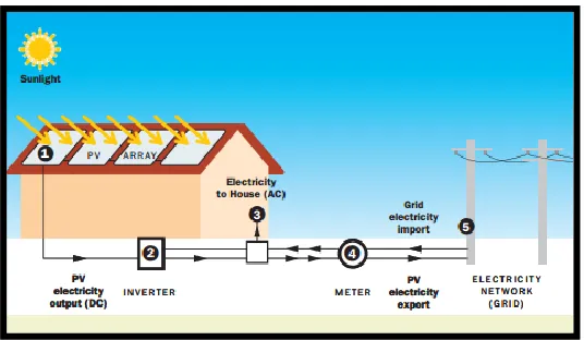
![Figure 1.3: A HVDC power transmission. [5]](https://thumb-us.123doks.com/thumbv2/123dok_us/94271.8869/19.612.154.498.71.199/figure-a-hvdc-power-transmission.webp)
![Figure 2.1: Half-bridge Single-phase VSI [7]](https://thumb-us.123doks.com/thumbv2/123dok_us/94271.8869/23.612.242.423.88.215/figure-half-bridge-single-phase-vsi.webp)
![Figure 2.3: Three-phase VSI [7]](https://thumb-us.123doks.com/thumbv2/123dok_us/94271.8869/24.612.205.422.476.700/figure-three-phase-vsi.webp)
