SUBTRACTION AND ADDITION DESIGN USING FIELD PROGRAMMABLE GATE ARRAY (FPGA)
MUHAMAD QAYUM BIN ABDULLAH
SUBTRACTION AND ADDITION DESIGN USING FIELD PROGRAMMABLE GATE ARRAY (FPGA)
MUHAMAD QAYUM BIN ABDULLAH
This Report Is Submitted In Partial Fullfillment Of Requirements For The Bachelor Degree of Electronic Engineering (Computer Engineering)
Fakulti Kejuruteraan Elektronik dan Kejuruteraan Komputer Universiti Teknikal Malaysia Melaka
UNIVERSTI TEKNIKAL MALAYSIA MELAKA
FAKULTI KEJURUTERAAN ELEKTRONIK DAN KEJURUTERAAN KOMPUTER
BORANG PENGESAHAN STATUS LAPORAN
PROJEK SARJANA MUDA II
Tajuk Projek : Subtraction and addition design using field programmable gate array
Sesi Pengajian : 1 4 / 1 5
Saya MUHAMAD QAYUM BIN ABDULLAH
(HURUF BESAR)
mengaku membenarkan Laporan Projek Sarjana Muda ini disimpan di Perpustakaan dengan syarat-syarat kegunaan seperti berikut:
1. Laporan adalah hakmilik Universiti Teknikal Malaysia Melaka.
2. Perpustakaan dibenarkan membuat salinan untuk tujuan pengajian sahaja.
3. Perpustakaan dibenarkan membuat salinan laporan ini sebagai bahan pertukaran antara institusi
pengajian tinggi.
4. Sila tandakan ( √ ) :
SULIT*
*(Mengandungi maklumat yang berdarjah keselamatan atau kepentingan Malaysia seperti yang termaktub di dalam AKTA RAHSIA RASMI 1972)
TERHAD** **(Mengandungi maklumat terhad yang telah ditentukan oleh organisasi/badan di mana penyelidikan dijalankan)
TIDAK TERHAD
Disahkan oleh:
__________________________ ___________________________________
iii
“Saya akui laporan ini adalah hasil kerja saya sendiri kecuali ringkasan dan petikan yang tiap-tiap satunya telah saya jelaskan sumbernya.”
Tandatangan : ……….
Nama Penulis : Muhamad Qayum bin Abdullah.
iv
“Saya/kami akui bahawa saya telah membaca karya ini pada pandangan saya/kami karya ini adalah memadai dari skop dan kualiti untuk tujuan penganugerahan Ijazah Sarjana
Muda Kejuruteraan Elektronik (Kejuruteraan Komputer).”
Tandatangan : ……….
Nama Penyelia : En. Anuar bin Jaafar
v
ABSTRAK
Projek ini adalah untuk merekabentuk perisian dan perkakasan simulasi untuk
litar penolakan dan tambahan melalui Field Programmable Gate Array(FPGA).Litar
lapan bit yang terlibat dalam melaksanakan penolakan dan penambahan yang dipilih
untuk setiap bit melalui perlaksanaan aritmetik dan logik unit, yang dikenali sebagai
Aritmetik Logik Unit (ALU). Semua hasil dari algorima ini akan dipamerkan di tujuh
segmen menggunakan papan FPGA dengan menggunakan Bahasa Verilog. FPGA adalah
alat semikonduktor, yang mengandungi komponen logik boleh atur cara yang dipanggil
"logik blok", dan antara hubungan yang boleh diatur cara. Logik blok juga boleh
diprogramkan untuk melaksanakan fungsi logik asas seperti AND, dan XOR, atau fungsi
gabungan yang lebih kompleks seperti dekoder atau fungsi matematik yang mudah
seperti tambah, tolak, darab dan bahagi (+, -, x, +). Kesimpulannya, lapan bit penolakan
vi
ABSTRACT
This project is about to design the software and hardware simulator for a eight bit
subtraction and addition circuit via Field Programmable Gate Array (FPGA). The eight
bit circuits are involved in performing the subtraction and addition selected for each bit
by performs operation the arithmetic and logic unit, called the Arithmetic Logic Unit
(ALU). All this operation is to be displayed at seven segment using FPGA board by using
Verilog Language. A FPGA is a semiconductor device, containing programmable logic
components called “logic blocks”, and programmable interconnects. Logic blocks can be
programmed to perform the function of basic logic gates such as AND, and XOR, or
more complex combinational functions such as decoders or simple mathematical
functions such as addition, subtraction, multiplication and divisions (+,-,x,+). In
conclusion, eight bit subtraction and addition circuit via FPGA has been successfully
vii
TABLE OF CONTENTS
CHAPTER TOPIC PAGE
ABSTRAK v
ABSTRACT vi
TABLE OF CONTENTS vii
LIST OF TABLES x
LIST OF FIGURES xi
LIST OF SYMBOL/ABBREVIATION/TERM xiii
I INTRODUCTION 1
1.1 PROJECT INTRODUCTION 1
1.2 PROJECT OBJECTIVES 2
1.3 PROBLEM STATEMENT 2
1.4 SCOPE OF WORK 3
1.5 METHODOLOGY 3
II LITERATURE REVIEW 5
2.1 THREE BIT SUBTRACTION CIRCUIT VIA
FIELD PROGRAMMABLE GATE ARRAY 5
2.2 HARDWARE MODELLING OF BINARY
viii
2.3 PERFORMANCE ANALYSIS OF DIFFERENT
BIT CARRY LOOK AHEAD ADDER USING
VHDL 8
TABLE OF CONTENTS
CHAPTER TOPIC PAGE
2.4 DESIGN AND ANALYSIS OF 16-BIT FULL
ADDER USING SPARTAN-3 FPGA 10
2.5 VHDL DESIGN OF FPGA ARITHMETIC
PROCESSOR 11
2.6 SUMMARY OF PROJECTS REVIEW 13
III METHODOLOGY 15
3.1 FLOWCHART OF PROJECT FLOW 15
3.2 FLOWCHART OF PROJECT SCOPE 17
3.3 FLOWCHART OF SUBTRACTION
AND ADDITION ALGORITHM 18
IV RESULTS AND DISCUSSION 21
4.1 RESULTS AND DISCUSSION IN FINAL YEAR 21
PROJECT I
4.2 ADDITION AND SUBTRACTION 8-BIT 23
ix
CHAPTER TOPIC PAGE
4.2.1 ALGORITHM CHECKLIST 23
4.2.2 SEVEN SEGMENT DISPLAY 24
4.2.3 LED DISPLAY 27
4.2.4 DIP SWITCH 28
4.2.5 PUSHBUTTON SWITCH 28
4.2.6 ADDITION AND SUBTRACTION 8-BIT 29
ALGORITHM
4.2.7 ADDITION AND SUBTRACTION 8-BIT 35
ALGORITHM SIMULATION
4.3 SYNTHESIS PROCESS 36
4.3.1 DESIGN SUMMARY IN XILINX ISE 10.1 36
4.3.2 USER CONSTRAINT FILE IN XILINX 38
ISE 10.1
4.3.3 REGISTER TRANSFER LEVEL (RTL) 40
SCHEMATICS
4.4 SUBTRACTION AND ADDITION 41
ALGORITHM IMPLEMENTATION ON
XILINX SPARTAN II
V CONCLUSION AND RECOMMENDATION 47
x
5.2 RECOMMENDATION 47
REFERENCES 48
LIST OF TABLES
NUM TITLE PAGE
2.1 Comparison between each project review 13
4.1 Checklist for the addition and subtraction algorithm 23
4.2 Sample calculation for binary to decimal 26
4.3 Bit assigned on the LED display 27
4.4 Bit assigned on the DIP switch 28
4.5 Bit assigned on the DIP switch 28
4.6 Selector assigned on the Pushbutton switch 29
4.7 Comparison between regular computation and binary 34
computation
4.8 Design summary 36
4.9 Addition computation with hardware implementation 42
xi
LIST OF FIGURES
NUM TITLE PAGE
1.1 Project Flowchart in General 3
2.1 Block Diagram for three bit subtraction circuit design 5
2.2 RTL of 8-bit CLA with decoder 7
2.3 4-bit Carry Look Ahead Adder 8
2.4 16-Bit Composed of 4-Bit Adders Linked by Ripple
Carry Propagation 10
2.5 Hardware representation of an 8-bit ALU 11
3.1 Project flowchart 16
3.2 Flow chart for Scope of Work 17
3.3 Flowchart of 8-bit addition and subtraction algorithm 20
4.1 Relationship between materials and equipments 21
4.2 LPA 2900 trainer 22
4.3 Seven segment display 24
4.4 Decoder of enabling seven segment displays 25
4.5 Verilog code for seven segment displays 26
4.6 LED display on the trainer board 27
4.7 DIP switch 28
4.8 Pushbutton switch 29
4.9 Verilog code for input and output declaration 30
xii
NUM TITLE PAGE
4.11 Verilog code for negative input A 32
4.12 Verilog code for negative input B 33
4.13 Verilog code for positive input A and input B 34
4.14 Testbench simulation on Xilinx 35
4.15 User constraint file 38
4.16 Floorplan for input and output location 38
4.17 Floorplan for input and output location 39
4.18 Text based floorplan for input and output location 39
4.19 Text based floorplan for input and output location 40
4.20 Input output block diagram 41
xiii
LIST OF SYMBOL / ABBREVIATION / TERM
FPGA - Field Programmable Gate Array.
RAM - Random Access Memory.
IC - Integrated Circuit.
PIC - Programmable Interface Controller.
HDL - Hardware Description Language.
VHDL - Very High Speed Hardware Description Language.
LED - Light Emitting Diode.
BCD - Binary-coded-decimal.
RTL - Register Transfer Level.
1
CHAPTER I
INTRODUCTION
This chapter discussed on the introduction of the project Subtraction and Addition
Design using Field Programmable Gate Array (FPGA). The first part included the project
summary, objectives, scope of work, problem statement and methodology. The project
introduction is the summary of all the important parts inside this chapter. There will be
three objectives listed for this project. The problem statement stated on the problem
occurred and why this project is proposed. The scope of work focused on what this
project will likely involved and done until this project is successful. Last but not least, the
methodology parts discussing on the flowchart of the early plan of this project.
1.1 Project Introduction
Field Programmable Gate Array (FPGA) is an integrated circuit designed that can
be configured by the user or owner of the device according to what the user wants it to
do. As example user can program it to do speech recognition and computer hardware
emulation. The most common use of FPGA is in aerospace and defense, audio,
automotive, broadcast, consumer electronics, security, video & image processing, wired
communications and wireless communications. FPGA is capable of doing high speed
process or computing because it contain of large number of logic gates and Random
Access Memory (RAM). FPGA is commonly program by using VHSIC Hardware
2
regular programming language because it includes the ways of describing the propagation
of time and signal dependencies as of controlling each of the logic gates. Therefore, in
this project a Addition and Subtraction System in Field-Programmable Gate Array is
proposed through hardware description language (Verilog) without discrete components.
The scope of this project is to do computation on addition and subtraction for 8 bits
system. The system will be able to receive input thus produce the output for the chosen
computation whether additional or subtraction. The system will run by a standard clock
10MHz. A LP-2900 trainer board will be use to test the prototype with Xilinx FPGA
chip. A simple calculator based on FPGA is expected to be produced.
1.2 Project Objectives
The objective of this project is to develop subtraction and addition program using Verilog
programming language. Besides that the objective is to simulate, testing the program
using Modelsim and to implement the algorithm to hardware by using circuit board. Last
but not least is to analyze the results obtain from the simulation and implementation of
algorithm.
1.3 Problem Statement
The main problem of the FPGA is there is not many FPGA’s programmer and not
many programmers are interested in FPGA. FPGA is a potential electronic circuit as it
can be program to perform any task or instructions desired as long as a proper algorithm
of Verilog is done. FPGA is different to PIC in term of language based and the
performance; where FPGA is more flexible compare to PIC microcontroller. Besides that
3
1.4 Scope of Work
The scope work is mainly on designing 8-bit system of FPGA subtraction and
addition algorithm by using verilog programming language. Modelsim software is used to
simulate the program and test on FPGA board.
1.5 Methodology
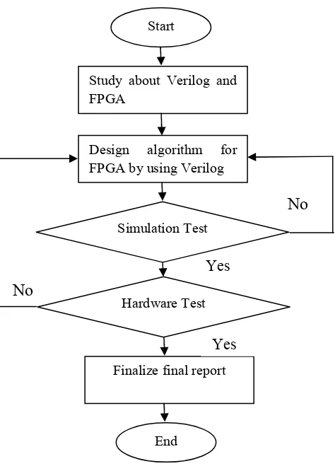
No
[image:17.612.217.454.275.608.2]No
Figure 1.1: Project Flowchart Yes Start
Study about Verilog and FPGA
Design algorithm for
FPGA by using Verilog
Simulation Test
Finalize final report
Final year project
End Hardware Test
4
Project flowchart in figure 1.1 is about the steps that will be taken in completing
the final year project. The first process is to study on Verilog and field programmable
gate array (FPGA). Literature review is will be done mostly on FPGA architecture, and
verilog language. Next process is to design subtraction and addition algorithm for FPGA
by using verilog language. Once the design is finished, the next step is to do simulation
test and hardware test. If both simulation and hardware test is success, the next process
can be proceed which is to finalize the final report for submission but if the simulation
and hardware test is fail, the design process for algorithm for FPGA by using verilog will
5
CHAPTER II
LITERATURE REVIEW
This chapter is about research and review on other works done by researchers that
are related to this project. This chapter contains six subtopics which are mostly related to
the scope of the final year project and also the details explanation of each of the literature
review. At the end of this chapter, a brief explanation and comparison between of the
final year project and the other existing work has been discussed thoroughly.
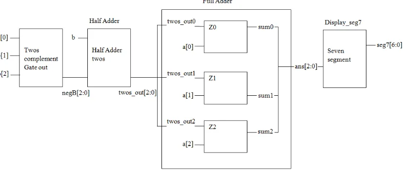
[image:19.612.119.532.443.619.2]2.1 Three Bit Subtraction Circuit via Field Programmable Gate Array.
6
The first literature review is about designing the software and hardware simulator
for a Three Bit Subtraction Circuit via Field Programmable Gate Array (FPGA). The
three bit subtraction circuits are involved in performing the subtraction for each bit by
performs operation the arithmetic and logic unit, called the Arithmetic Logic Unit.
Based on Figure 2.1, the block consists of 4 modules which are twos complement
gate not, half adder, full adder and seven segment display. The operation will be
displayed on the seven segment using FPGA board by using Verilog Language. The logic
blocks in the FPGA are used to perform the mathematical functions to do the subtraction
process between the two inputs of the three bit binary.
The first block diagram is twos complement gate not, which is to do 2’s
complement process on input B. At this block diagram input B is going through invert
process that converts from 1 to 0 and 0 to 1. The output for the first block diagram is
negB[2:0]. The next block diagram is Half adder twos which is to add 1 to the negB[2:0]
and resulting to 2’s complement process. The output for the Half Adder block is
twos_out[2:0].
The third block diagram is Full Adder where the subtraction process is done.
Input A and the 2’s complement of input B (twos_out[2:0]) will be added together and
produce the output of ans[2:0]. The ans[2:0] is then will be send to the last block diagram
that is Display_seg7 to display the output on the seven segment display.
As a conclusion, Figure 2.1 is about three bit subtraction for Field Programmable
Gate Array. It shows the steps of designing the three bit subtraction starting from the
software part until the hardware part. The algorithm is tested by using software
7
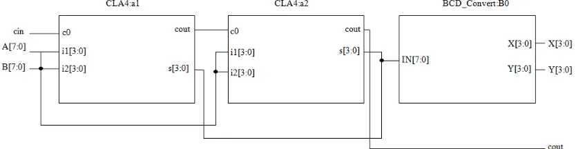
[image:21.612.116.533.111.219.2]2.2 Hardware Modeling of Binary Coded Decimal Adder in FPGA.
Figure 2.2: RTL of 8-bit CLA with decoder.
Next literature review is “Hardware Modellng of Binary Coded Decimal Adder in
FPGA (October 2012)” by Muhammad Ibn Ibrahimy, MD. Rezwanul Ahsan, and
Iksannurazmi. It is about comparing the carry look ahead and the ripple carry in adder
arithmetic for Field Programmable Gate Array (FPGA) and also to illustrate the design
and hardware modeling of a BCD adder. The successful functional and timing simulation
of the CLA based BCD adder, the design is then continued to the physical FPGA device
which is the Altera DE2 board (Altera Cyclone II 2C35 FPGA device).
In this literature review also explain on how does the R-C adder operation and
CLA adder operation in compute the addition carry and forward it to a subsequent adder.
The simulation for RC adder and CLA adder is done, where the result is analyzed in term
of timing to observe which adder type has the best performance.
Basically, the concept of having R-C is to let each adder compute a carry and
forward it to a subsequent adder. One way to improve this method is by having an
algorithm to pre-calculate the carries before forwarding the sum Co the next adder.
Therefore, such implementation can be done in CLA by expediting the carry propagation
and eliminating the inter stage carry delay. To invoke this algorithm (Reese and
Thornton, 2006), carry propagate as well as carry generate are being used.
Based on the RTL in the Figure 2.2 above, it starts with two inputs (8-bit) from
8
which process 4-bit addition for the input A and input B, the output for this block
diagram is cout that will go to the next block diagram and s[3:0] will go to
BCD_Convert:B0.
The second block diagram is CLA4:a2 which do similar process as the first block
diagram. The input is the rest bit from input A and input B and the output is s[3:0] and
cout. The cout will the output carry bit of the process, meanwhile the output from block
CLA4:a1 and CLA4:a2 will go to next BCD_Convert:B0.The generated binary number is
then converted into BCD. The conversion process has been done by implementing a
decoder and the output is then sent to 7-segment display in Altera DE-2 board FPGA.
As the conclusion, this article is a good reference for the final year project as it
provides a proper guideline in designing adder algorithm from the software simulation
and analysis until the hardware implementation for the real world FPGA device.
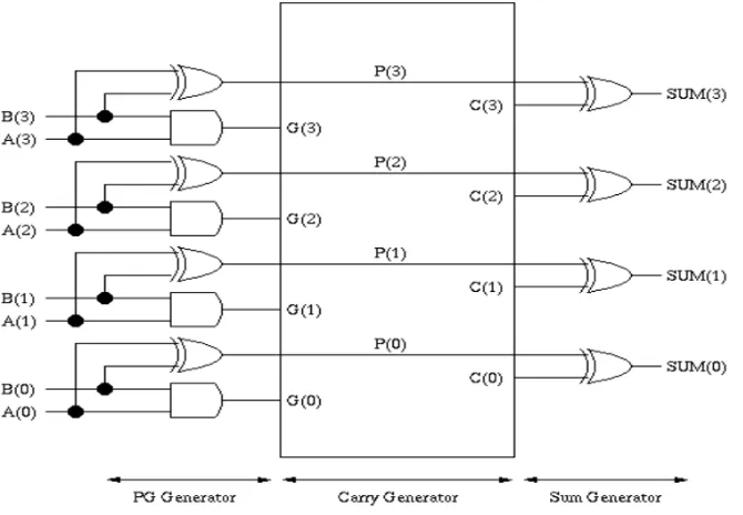
[image:22.612.162.497.438.670.2]2.3 Performance Analysis of Different Bit Carry Look Ahead Adder Using VHDL.
9
Next literature review will discusses all the available adders’ type for their
implementation with good attributes and some drawbacks. However this article will focus
more on the implementation and simulation of 4-bit, 8-bit and 16-bit carry look ahead
adder based on the Very High Speed Integrated Circuit Hardware Description Language
(VHDL).
A carry-lookahead adder improves speed by reducing the amount of time required
to determine carry bits. It can be contrasted with the simpler, but usually slower, ripple
carry adder for which the carry bit is calculated alongside the sum bit, and each bit must
wait until the previous carry has been calculated to begin calculating its own result and
carry bits. The carry-lookahead adder calculates one or more carry bits before the sum,
which reduces the wait time to calculate the result of the larger value bits.
Based on Figure 2.3, on the left side is the bits used in the design which is 4-bit
and the input is A and B. Then, the input move to the carry generator which is the carry
looks ahead process. The right side is where the summations is made and send it to the
output. The propagate 'Pi' and generate 'Gi' in a full adder is given by Pi which is equal to
x_in xor operation with y_in Carry propagate while Gi equal to x_in and operation with
y_in Carry generate. Both propagate and generate signals depend only on the input bits
and thus will be valid after one gate delay.
The new expressions for the output sum and the carryout are given by sum equal
to Pi xor operation with Ci-1 and carry_out is equal to Gi + Pi and operation with Ci.
Carry signal will be generated when both bits x_in and y_in is equal to 1 and either x_in
or y_in is equal to 1 with the carry_bit is equal to 1. For example for 4-bit operation x_in
is 1H, y_in is 5H and the carry_in is 1H. The sum operation from the algorithm will
produce 7H by adding x_in, y_in and carry_in together meanwhile the carry_out is 0H.
As the conclusion, the article shows on how to design a 4-bit carry look ahead
adder from the design specification, simulation process, synthesis process, physical
10
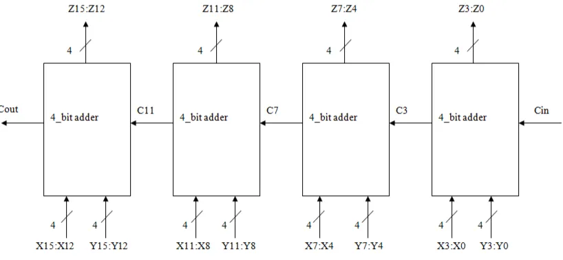
[image:24.612.120.529.109.298.2]2.4 Design and analysis of 16-bit Full Adder using Spartan-3 FPGA.
Figure 2.4: 16-Bit Composed of 4-Bit Adders Linked by Ripple Carry Propagation
This literature review is about designing High-Speed adders especially in
Semi-Custom designs because the technique that is used in the design of various n-bit is
different. The purpose of designing fast adders is to reduce the time required to form
carry signals. The objecitve is to implement 4-bit Carry Look Ahead adder with the
VHDL primitive and to prove that VHDL is implemented as optimized 4-bit CLA and
can be use to develop n-bit adder. By using carry look-ahead mechanism, the propagation
delay is reduced to four-gate level irrespective of the number of bits in the adder
From the Figure 2.4, each block is linked with each other for the ripple carry
propagation and forming 16-bit adder. Four 4-bit CLAs are interconnected as ripple adder
form as shown in the figure 2.4, here the carry is propagated to the next stage 4-bit CLA.
The internal carry propagation delay of 4-bit adder is reduced by using the technique
CLA. So that the overall speed of the 16-bit Adder is increased. The input will be X and
Y, while the output is Z and Cout as its carry.
The input for the system is 16-bit where each 4_bit adder block will get 4-bit
input of input x and input y. The cin will go through from the first 4_bit adder and
continue to the next 4_bit adder block until the last 4_bit adder block where the results of