Rochester Institute of Technology
RIT Scholar Works
Theses
8-2019
Design and Verification of a DFI-AXI DDR4
Memory PHY Bridge Suitable for FPGA Based
RTL Emulation and Prototyping
Pallavi Avinash Mayekar
Follow this and additional works at:https://scholarworks.rit.edu/theses
This Thesis is brought to you for free and open access by RIT Scholar Works. It has been accepted for inclusion in Theses by an authorized administrator of RIT Scholar Works. For more information, please [email protected].
Recommended Citation
DFI-AXI DDR4 M
EMORY
PHY B
RIDGE
S
UITABLE FOR
FPGA B
ASED
RTL E
MULATION AND
P
ROTOTYPING
DESIGN ANDVERIFICATION OF ADFI-AXI DDR4 MEMORY PHY BRIDGE
SUITABLE FOR FPGA BASEDRTL EMULATION ANDPROTOTYPING
BY
PALLAVIAVINASHMAYEKAR
A THESIS
SUBMITTED IN PARTIAL FULFILLMENT
OF THE REQUIREMENTS FOR THE DEGREE OF
MASTER OFSCIENCE
INELECTRICALENGINEERING
DEPARTMENT OFELECTRICAL AND MICROELECTRONICENGINEERING
KATE GLEASONCOLLEGE OFENGINEERING
ROCHESTER INSTITUTE OF TECHNOLOGY
ROCHESTER, NEWYORK
PALLAVIAVINASHMAYEKAR
Committee Approval:
We, the undersigned committee members, certify that Pallavi Avinash Mayekar has completed the requirements for the Master of Science degree in Electrical Engineering.
Mr. Mark A. Indovina,Graduate Research Advisor Date
Senior Lecturer, Department of Electrical and Microelectronic Engineering
Dr. Dorin Patru Date
Associate Professor, Department of Electrical and Microelectronic Engineering
Dr. Dan Phillips Date
Associate Professor, Department of Electrical and Microelectronic Engineering
Dr. Sohail Dianat,Department Head Date
I would like to dedicate this work to my family, my grandparents, my father Avinash, my
mother Anjali, my sister Pooja, my brother Vaibhav, and friends for their unconditional love and
I hereby declare that except where specific reference is made to the work of others, that all
content of this Graduate Thesis is original and have not been submitted in whole or in part for
consideration for any other degree or qualification in this, or any other University. This Graduate
Thesis is the result of my own work and includes nothing which is the outcome of work done in
collaboration, except where specifically indicated in the text.
Pallavi Avinash Mayekar
Acknowledgements
I am very grateful to my advisor Professor Mark A. Indovina, for providing guidance and
feed-back during these past three years. Mark is one smartest people I know who also makes learning
fun. He is my best role model for an engineer, teacher, and mentor. Mark was the reason why I
decided to go and pursue a career in Digital design and verification. Thank you for all the
sup-port and encouragement. I would like to thank Chris Browy and Chilai Huang of Avery Design
Systems as the motivation behind this project, for their helpful suggestions, and for providing
access, and licenses to the Avery VIP discussed in this paper. Chris was a primary source for
getting certain specification related questions answered. I would also like to thank the members
of my thesis committee, Dr. Dorin Patru, and Dr. Dan Phillips for their feedback, helpful career
advice and general suggestions. I also thank all professors whose knowledge and experience
System on chip (SoC) designers today are emphasizing on a process which can ensure robust
silicon at the first tape-out. Given the complexity of modern SoC chips, there is compelling
need to have suitable run time software, such at the Linux kernel and necessary drivers available
once prototype silicon is available. Emulation and FPGA prototyping systems are exemplary
platforms to run the tests for designs, are naturally efficient and perform well, and enable early
software development. While useful, one needs to keep in mind that emulation and FPGA
pro-totyping systems do not run at full silicon speed. In fact, the SoC target ported to the FPGA
might achieve a clock speed less than 10 MHz. While still very useful for testing and software
development, this low operating speed creates challenges for connecting to external devices such
as DDR SDRAM. In this paper, the DDR-PHY INTERFACE (DFI) to Advanced eXtensible
In-terface (AXI) Bridge is designed to support a DDR4 memory sub-system design. This bridge
module is developed based on the DDR PHY Interface version 5.0 specification, and once
imple-mented in an FPGA, it transfers command information and data between the SoC DDR Memory
controller being prototypes, across the AXI bus to an FPGA specific memory controller
con-nected to a DDR SDRAM or other physical memory external to the FPGA. This bridge module
enables multi-communication with the design under test (DUT) with a synthesizable SCE-MI
based infrastructure between the bridge and logic simulator. SCE-MI provides a direct
mecha-nism to inject the specific traffic, and monitor performance of the DFI-AXI DDR4 Memory PHY
Contents
Contents v
List of Figures ix
List of Tables xi
Glossary xiv
1 Introduction 1
1.1 Research Goals . . . 4
1.2 Contributions . . . 4
1.3 Thesis Organization . . . 5
2 Background Research 6 2.1 DDR memory sub-system . . . 8
2.1.1 DDR Memory . . . 10
2.1.2 DDR Memory Controller . . . 15
2.1.3 DDR4 PHY . . . 16
2.2 AXI Protocol . . . 16
2.4 UVM for Verification . . . 22
3 Architecture Overview 25 3.1 SoC (DUT) Memory Controller . . . 26
3.2 DFI . . . 26
3.2.1 Interface Group . . . 27
3.2.1.1 Command Interface . . . 27
3.2.1.2 Write Data Interface . . . 32
3.2.1.3 Read Data Interface . . . 32
3.2.1.4 Update Interface . . . 38
3.2.1.5 Status Interface . . . 43
3.2.1.6 Low Power Control Interface . . . 47
3.2.1.7 Error Interface . . . 50
3.2.1.8 PHY Master Interface . . . 52
3.2.1.9 Disconnect Protocol . . . 56
3.2.1.10 2N Mode Interface . . . 56
3.2.1.11 MC to PHY Message Interface . . . 57
3.2.1.12 WCK Control Interface . . . 57
3.3 DFI-AXI DDR4 Memory PHY Bridge . . . 59
3.3.1 Command Transaction Unit . . . 59
3.3.1.1 Initialization Unit . . . 59
3.3.1.2 Control Unit . . . 60
3.3.1.3 Decode Command Unit . . . 60
3.3.2 Write Transaction Unit . . . 61
Contents vii
3.3.2.2 Write FIFO . . . 62
3.3.3 Read Transaction Unit . . . 63
3.3.3.1 Read FSM . . . 63
3.3.3.2 Read FIFO . . . 65
3.3.4 Interactions Unit . . . 65
3.3.4.1 DFI interactions FSM . . . 65
3.3.4.2 SCE-MI Controller . . . 68
3.4 SCE-MI . . . 68
3.5 AXI Master transactor . . . 69
3.5.1 AXI Write Channel . . . 69
3.5.2 AXI Read Channel . . . 74
3.6 AXI . . . 78
3.6.1 Write Address Channel . . . 78
3.6.2 Write Data Channel . . . 79
3.6.3 Write Response Channel . . . 79
3.6.4 Read Address Channel . . . 80
3.6.5 Read Response Channel . . . 81
4 Verification Environment 82 4.1 Testbench Architecture . . . 82
4.1.1 Testbench Architecture with DDR Memory Subsystem . . . 82
4.1.2 Testbench Architecture with AXI Slave . . . 84
4.2 Coverage . . . 85
5 Results and Discussion 86
5.1 Testcase Scenario . . . 86
5.2 Simulation Results . . . 87
5.3 Coverage Results . . . 93
6 Conclusion 94
6.1 Futurework . . . 95
List of Figures
2.1 DRAM Top Level Diagram . . . 7
2.2 Decoding Row and Column Address Fields [1] . . . 8
2.3 DDR Memory Sub-system [2] . . . 9
2.4 State Diagram of DDR4 [3] . . . 13
2.5 Block diagram of Memory Controller [4] . . . 14
2.6 Write Transaction Channel Architecture . . . 18
2.7 Read Transaction Channel Architecture . . . 18
2.8 Standard OOP Testbench Architecture . . . 23
3.1 System-level Architecture of Memory Sub-system . . . 25
3.2 Block diagram of DDR PHY Interface signals [5] . . . 28
3.3 Write Finite State Machine . . . 62
3.4 Read Finite State Machine . . . 64
3.5 DFI Interactions State Machine . . . 66
3.6 AXI Write Channel Master Transactor Block Diagram [6] . . . 70
3.7 AXI Read Channel Master Transactor Block Diagram [6] . . . 74
3.8 AXI Write Address Message . . . 78
3.10 AXI Write Response Message . . . 80
3.11 AXI Read Address Message . . . 80
3.12 AXI Read Response Message . . . 81
4.1 Top-level Verification Architecture with DDR4 Memory Subsystem . . . 83
4.2 Top-level Verification Architecture with AXI Slave VIP . . . 84
5.1 Write Interface Signal Transaction with Burst of 8 . . . 86
5.2 Read Interface Signal Transaction with with Burst of 8 . . . 87
5.3 Write Address Transaction with 2 Independent Writes . . . 88
5.4 Write Data Transaction with Burst of 8 . . . 88
5.5 Read Address Transaction With 2 Independent Reads . . . 89
5.6 Read Data Transaction with Burst of 8 . . . 89
5.7 Write Data Interface Simulation Waveforms . . . 91
5.8 Read Data Interface Simulation Waveforms . . . 92
List of Tables
2.1 DRAM Input And Output Pins [3,7] . . . 7
2.2 Comparing DDR family [8] . . . 11
2.3 DDR Command table [3,5,7,9] . . . 14
2.4 OOP Testbench Components [10] . . . 19
2.4 OOP Testbench Components [10] . . . 20
2.4 OOP Testbench Components [10] . . . 21
2.4 OOP Testbench Components [10] . . . 22
3.1 Command Interface Signals [5] . . . 29
3.1 Command Interface Signals [5] . . . 30
3.1 Command Interface Signals [5] . . . 31
3.1 Command Interface Signals [5] . . . 32
3.2 Command Interface Timing Parameters [5] . . . 33
3.4 Write Data Interface Signals [5] . . . 34
3.5 Write Data Interface Timing Parameters [5] . . . 35
3.6 Read Data Interface Signals [5] . . . 36
3.7 Read Data Interface Timing Parameters [5] . . . 37
3.8 Update Interface Signals [5] . . . 39
3.8 Update Interface Signals [5] . . . 40
3.8 Update Interface Signals [5] . . . 41
3.9 Update Interface Timing Parameters [5] . . . 42
3.10 Status Interface Signals [5] . . . 43
3.10 Status Interface Signals [5] . . . 44
3.10 Status Interface Signals [5] . . . 45
3.11 Status Interface Timing Parameters [5] . . . 46
3.12 Low Power Control Interface Signals [5] . . . 47
3.12 Low Power Control Interface Signals [5] . . . 48
3.12 Low Power Control Interface Signals [5] . . . 49
3.12 Low Power Control Interface Signals [5] . . . 50
3.13 Low Power Control Interface Timing Parameters [5] . . . 51
3.14 Error Interface Signals [5] . . . 51
3.15 Error Interface Timing Parameters [5] . . . 51
3.16 PHY Master Interface Signals [5] . . . 52
3.16 PHY Master Interface Signals [5] . . . 53
3.16 PHY Master Interface Signals [5] . . . 54
3.17 PHY Master Interface Timing Parameters [5] . . . 55
3.18 Disconnect Protocol [5] . . . 56
3.19 Disconnect Protocol Timing Parameters [5] . . . 56
3.20 2N Mode Interface Signals [5] . . . 56
3.21 2N Mode Interface Timing Parameters [5] . . . 57
3.22 MC to PHY Message Interface Signals [5] . . . 57
List of Tables xiii
3.24 WCK Control Interface Signals [5] . . . 58
3.25 WCK Control Interface Timing Parameters [5] . . . 58
3.26 Truthtable of DFI Interaction Signals . . . 67
3.27 Write Channel SFR Registers [6] . . . 73
3.28 Read Channel SFR Registers [6] . . . 77
5.1 Frequency Mode . . . 87
5.2 Write Requests . . . 87
Acronyms
AMBA Advanced Microcontroller Bus Architecture
ARM Advanced RISC Machine
ASIC Application-specific Integrated Circuit
AXI Advanced eXtensible Interface
CAS Column Address Strobe
CDC Clock Domain Crossing
DDR Double data rate
DFI DDR-PHY Interface
DUT Device Under Test
FPGA Field Programmable Gate Array
HDL Hardware Description Language
Glossary xv
IMC Integrated Metric Center
JEDEC Joint Electron Device Engineering Council (JEDEC) Solid State Technology
As-sociation
MC Memory Controller
OOP Object-oriented Programming
RAS Row Address Strobe
RTL Register-Transfer Level
SDRAM Synchronus Dynamic Random-Access Memory
SoC System on Chip
TLM Transaction Level Modeling
UVM Universal Verification Methodology
VIP Verification Intellectual Property
Introduction
Modern SoC (System on Chip) and ASICs (Application-Specific Integrated Circuits) are the size
of a fingernail, and this approximate silicon area contains billions of transistors. Due to the high
levels of integration and automated manufacturing, the cost of these transistors has fallen to a
tiny fraction of a cent. That refinement – the simple premise that chips would perform more and
cost less – helped the industry bring staggering discovery to the world, from personal computers,
smartphones, to the power of the Internet [11]. However, the demand for more performance is
leading to chips loaded with a large number of features and an increase in the size of the designs.
Chips are getting bigger and bigger in terms of gate counts in conjunction with supported
fea-tures. In such a framework, the primary goal is to achieve rigid time-to-market and to perform
adequate verification of such large designs.
The process of creating ICs (Integrated Circuits) by combining billions of transistors onto
one single chip is called VLSI (Very Large Scale Integration). Digital designers often use
Ver-ilog or SystemVerVer-ilog HDL (Hardware description language) to describe the functionality of
the ICs [12]. VLSI level technology began in the year of 1970s while developing the earliest
2
the introduction to VLSI technology, most ICs performed a fixed, limited set of functions. VLSI
technology allows designers to often include memory blocks such as RAM, ROM, flash memory,
EEPROM, multiple processors cores, and other logic blocks into a single chip.VLSI technology
defines a specific design flow for SoC, ASIC, or large scale FPGA (Field Programmable Gate
Array) designs. The stages in the design flow are the unique combination of EDA (Electronic
Design Automation) tools to achieve the design of an integrated circuit. This design process
consists of multiple stand-alone stages for design closure before tape out and semiconductor
manufacture. Moore’s Law1has benefited from the entire IC implementation flow, from RTL to
GDSII starting with specification followed by high-level design, low-level design, RTL coding,
functional verification, logic synthesis, placement and routing, gate level simulation, fabrication,
and post-silicon validation [13]. FPGA prototyping and emulation for RTL/Virtual Acceleration
leverages a similar design process and tools, enabling engineers to integrate HW/SW earlier and
deploy more widely lower cost/risk alternatives [14].
Multiple solutions spanning the design flow process, i.e., pre-silicon, prototype, and
post-silicon requires retargeting the design numerous times. Retargeting and updating the design
many times requires tools, expertise, and engineers to explore trade-offs to achieve a
satisfac-tory result. This effort does not translate into predictable, repeatable outcomes. To support
these challenges and to make functional verification closure, emulation for RTL acceleration and
expanding FPGA prototyping technologies can be performed. Emulation allows the use of a
specialist hardware and software and maps automatically from design’s RTL representation to
an internal programmable gate-array to perform the functional verification of both hardware and
software parts of the design. It also allows integration of hardware and software at a very early
stage and to leverage the same resource of the design process, tools, and engineers. Emulation is
1Moore’s law is the prediction by engineer Gordon Moore that the number of transistors per silicon chip will double
an alternative with the lowest cost and risk [15–17].
There is a constant demand for computer memories to be low powered, faster, more extensive
in the capacity size, and smaller in physical size. These never-ending list of requirements is
re-sponsible for the advancement of DRAM (Dynamic random-access memory) Technology. With
several technology enhancements, DRAMS have evolved into SDRAM (Synchronous DRAM),
DDR (Double Data Rate) SDRAM, DDR2 (Double Data Rate 2) SDRAM, DDR3 (Double Data
Rate 3) SDRAM, DDR4 (Double Data Rate 4) SDRAM. DDR4 SDRAMs are very pervasive in
devices that use FPGAs and ASICs [18,19].
This design and verification work proposes a DDR-PHY INTERFACE (DFI) to Advanced
eXtensible Interface (AXI) Bridge is developed supporting DDR4 SDRAM memory sub-system
design suitable for use in FPGA prototype and RTL Emulation (FPGA-based) [5]. Pre-silicon
emulation of DDR4 catches bugs in the early stage to eliminate propagating errors to silicon.
The DFI-PHY interface protocol is the industry standard for DDRx and HBM memory controller
to a PHY signal interface developed by Denali/Cadence. AXI is the popular AMBA interface
interconnect developed by ARM [20].
Since the SoC DUT ported to the FPGA prototype would not run at full operating speed,
a speed bridge is required. Another challenge porting the SoC DUT to the FPGA is choice
of components provided by the FPGA platform. For example, the Xilinx DDR PHY is not
DFI compliant, and therefore a direct connection to the SoC DUT memory controller is not
possible. The DFI-AXI DDR4 Memory PHY Bridge solves both these problems by handling
clock domain crossing and providing an accurate DFI-PHY interface to SoC DUT. With the
DFI-AXI DDR4 Memory PHY Bridge providing physical memory access to the prototype SoC
memory controller, the prototype SoC behaves as if it is connected to DDR4 operating at full
speed. With the addition of the bridge module in the architecture, the system will be more
1.1 Research Goals 4
1.1
Research Goals
The goals of this research is to research, design, and verification DFI-AXI DDR4 Memory PHY
Bridge supporting external DDRx/HBM memory sub-systems; the resultant design will be
suit-able for use in FPGA prototype and RTL Emulation (FPGA-based). The following objectives
are the primary objects of this research:
• To understand the requirements of a DFI-AXI DDR4 Memory PHY Bridge.
• To design the RTL design for the DFI-AXI DDR4 Memory PHY Bridge.
• RTL and gate level verification or the DFI-AXI DDR4 Memory PHY Bridge using
Sys-temVerilog testbench environment incorporating Avery DDR, AXI, and I2C Verification
Intellectual Property (VIP).
• Perform logic synthesis of the DFI-AXI DDR4 Memory PHY Bridge design with suitable
timing and environment constraints.
• To develop a system to collect the verification coverage results and represent them
graphi-cally.
1.2
Contributions
The significant contributions to the project are as follows:
1. Research and development of a DFI-AXI DDR4 Memory PHY Bridge module that
cap-tures all DFI transactions, processes, and forwards these transactions at AXI transactions
2. Integrated asynchronous FIFOs to reliably pass signals between two different clock domain
of DFI and AXI.
3. Verified the design by writing a SystemVerilog based testbench.
(a) Development of verification components such as assertions, etc., to the observe and
validate the behavior of the DFI-AXI DDR4 Memory PHY Bridge.
1.3
Thesis Organization
The structure of the thesis is as follows:
• Chapter2: This chapter discusses the literature and methodology that are referred to
pro-vide a foundation for the research, design, and development of the DFI-AXI DDR4
Mem-ory PHY Bridge module suitable for Emulation and FPGA prototyping.
• Chapter 3: The chapter discusses the system level and DFI-AXI DDR4 Memory PHY
Bridge module architecture.
• Chapter4: This verification environment used to test the DFI-AXI DDR4 Memory PHY
Bridge module is discussed in this chapter.
• Chapter5: This chapter outlines the results of this work.
Chapter 2
Background Research
This chapter discusses the essential theories and concepts related to the DFI-AXI DDR4 Memory
PHY Bridge module.
DRAM (Dynamic Random-Access Memory) memory has dominated as the core system
memory in computers, smartphones, and high-end serves for a long time [21]. Figure2.1shows
the top level of the DRAM. The DRAM consists of essential Input/Outputs like a clock, reset,
data, chip select, and address. The Table2.1 has more details about the Input and Output pins.
During a write operation, data flows from the controller to DRAM and on a read operation from
DRAM to the controller. Considering that data flows in both directions to and from the DRAM,
the data signals go hand in hand with the data strobe signal to control the bi-directional nature
[11].
To write into the memory, user provides address and the data, and to read from the memory,
the user provides the address. In modern virtual memory systems, the address provided by the
user is called the logical address. Before sending an address to DRAM, this logical address gets
translated to a physical address. Once processed by the memory controller, the physical address is
Figure 2.1: DRAM Top Level Diagram
Table 2.1: DRAM Input And Output Pins [3,7]
Symbol Type Function
RESET_n Input If high, DRAM is active
CS_n Input If low, memory looks at all other inputs
CKE Input If high, internal clock signals are active
CK_t/CK_c Input Differential clock inputs
DQ, DQS Inout Strobe controls the data bus
RAS_n, CAS_n, WE_n Input Dual function input pins.
ACT_n Input Pins indicates read or write command.
BG0-1, BA0-1 Input Bank group and bank address input
2.1 DDR memory sub-system 8
from or write to derives from these individual fields. Figure2.2shows decoding row and column
address fields. On identifying the bank and bank group, the row part of the address activates a line
called word line in the memory array. The word line reads data from the memory array into sense
amplifiers. The bit line is the width of the column. The column address then reads part of the
word from sense amplifier. The DRAMs are classified based on the column width such as x4, x8,
or x16, which directly relates to device bit width. Given the nature of memory systems and the
need for uniformity, DRAM are standardized by JEDEC [7]. For example, JEDEC specification
JESD209-4B defines the LPDDR4 standard, including functionality, features, characteristics,
[image:27.612.109.506.318.545.2]ball assignments, and packages [24,25].
Figure 2.2: Decoding Row and Column Address Fields [1]
2.1
DDR memory sub-system
Due to the nature of the physical interface, SoC, ASIC or FPGA designs typically cannot talk
the help of a DDR memory sub-system which contains the following components and is shown
in Figure2.3.
• DDR Memory
• DDR Memory Controller
• DDR PHY
Figure 2.3: DDR Memory Sub-system [2]
The DDR memory shown is the typically soldered down on the printed circuit board [26].
SoC, ASIC, or FPGA designs are comprised of DDR memory controller, DDR PHY, user-logic,
and other minor blocks. The user defines the interface be user-logic and DDR memory controller.
On requesting a write or read to the memory controller, the user-logic issues a logical address.
The memory controller is responsible for converting the physical address and forwarding the
address fields to the DDR PHY. A standard interface called DFI interface allows communication
between the DDR memory controller and DDR PHY [27]. Then DDR PHY performs all lower
2.1 DDR memory sub-system 10
2.1.1
DDR Memory
A DDR is an updated version of SDRAM, and in modern systems, a memory subsystem consists
of multiple DDR chips with a common clock, address and command line. In this configuration, a
DDR interface presupposes multiple DDR chips that transfer data to/from the memory controller
via several data lines. As apposed to single data rate SDRAM, DDR is double data rate memory
because the data is transferred twice per clock, a data sample transmits on the rising edge of the
clock, and another data sample transmits on the falling edge of the clock. The SDRAM could
only manage to transfer one transaction per clock. Whereas, here in DDR, the clock runs at half
of the DDR data rate and supplied to all DRAMs. DDR1 has 4 banks, 2 bank address bits, DDR2
and DDR3 have 4 or 8 banks, 2 or 3 bank address bits. DDR4 SDRAM is the current member of
the DDR family. DD4 is focusing on data reliability. The table2.2shows the comparison of the
Table 2.2: Comparing DDR family [8]
Features DDR SDRAM DDR2 SDRAM DDR3 SDRAM DDR4 SDRAM
Clock
Frequency
100 / 133 / 166 /
200 MHz
200 / 333 / 400
MHz
400 / 533 / 667 /
800 MHz
800 / 1600 /
1866 / 2133
MHz Clock Input Differential clock Differential clock Differential clock Differential clock
I/O Width x4 / x8 / x16 /
x32
x4 / x8 / x16 x4 / x8 / x16 x4 / x8 / x16
Data Strobe Single data strobe Differential data strobe Differential data strobe Differential data strobe
Prefetch 2 bit 4 bit 8 bit 8 bit
Supply
Voltage
2.5V 1.8V 1.5V 1.2V
On Die
Termina-tion
(ODT)
Unsupported Supported Supported Supported
Burst
Length
2, 4, 8 4, 8 8, 4 (Burst chop) 8, 4 (Burst chop)
CAS
Latency
(CL)
2, 2.5, 3 clock 3, 4, 5 clock 5, 6, 7, 8, 9, 10
clock
5, 6, 7, 8, 9, 10
clock
2.1 DDR memory sub-system 12
has 16 banks, 4 bank group with 4 banks for each group, Row and Column address locates the
requested bank in the memory. A bank is an independent memory array. The page is a unique
address made of bank group, bank, and a row address. The size of a page is the number of bits
per row. If the column address is 10 bits wide, then there are 1K bit lines per row. Rank is
the highest logical unit and is used to increase memory capacity [19]. A single memory die of
16GB has one chip select (CS_n) signal, so it is called Single-Rank. If the same memory divides
into two 8GB, it is called Dual-Rank, or into four 4GB it is called Quad-Rank. The rank is also
known as depth cascading.
The DDR4 has six main signals in the command bus that control the operation of the DDR
interface. The memory starts operation with an activate command followed by a write or read
command [22]. Read and write operations can be single or burst oriented. In a single write
operation, for each data, an address is provided [30]. In a burst write operation, it starts writing
from the user provided address and continues for a burst length of eight or for a chopped burst
length of four [31]. The signals are clocked to the rising edge of the clock. The read (RD)
and write (WR) operation is a two-step process. An activate command (ACT) opens a row in a
bank and makes it accessible for succeeding write (WR) and read (RD) operations. Figure2.4
shows the state diagram for all the possible state transitions and controlling commands for DDR4
SDRAM. The activate (ACT) command selects the bank, bank group, and row to be activated.
This step is called RAS (Row Address Strobe). The step CAS (Column Address Strobe) accounts
the registered address bits and coincides it with RD or WR command. The command state also
includes preselect, precharge, no operation, refresh, activate, and mode register set commands.
The table 2.3 shows the command truth table. The precharge (PRE) command de-activates a
current open row. The de-activating of open rows can be done automatically after a write or
read operation is complete using write with auto precharge (WRA) and read with auto precharge
2.1 DDR memory sub-system 14
[image:33.612.85.534.88.346.2]Figure 2.5: Block diagram of Memory Controller [4]
Table 2.3: DDR Command table [3,5,7,9]
Function Code CS_n ACT_n RAS_n CAS_n WE_n AP
Refresh REF L H L L H H or L
Write WR L H H L L L
Read RD L H H L H L
Bank Activate ACT L L row address
Single Bank Precharge PRE L H L H L L
Write with Auto-Precharge WRA L H H L L H
2.1.2
DDR Memory Controller
A general memory controller is a digital circuit that masters the flow of data into/from the main
memory of the computer. Memory controller circuits integrate into another chip or can be a
separate chip itself. A memory controller is typically segmented into two parts: the controller
front-end and back-end. The front-end of the memory controller buffers requests and responses.
It is independent of the type of memory and provides an interface to the rest of the system.
The back-end of the memory controller is dependent on the type of memory and provides an
interface towards the target memory [33, 34]. memory mapping, arbiter, command generator,
and data path are four functional blocks of a memory controller, and are shown in Figure2.5.
Memory mapping is a translation between the logical address and physical memory. The
purpose of memory mapping is to decode logical address to physical address, to support memory
protection, and to advance the quality of memory management. The memory map decodes the
address by slicing into bank, row, and column. The period memory map takes to execute an
instruction and to run a set of programs determines the computer performance. At each time
when the program requests to the corresponding memory word by presenting a logical address,
the memory map must translate the logical address to physical address [35,36]. A more
straight-forward translation decreases the implementation cost and increases the performance of memory.
The total number of bits in a memory address determines the size of the logical address space.
In a large physical address memory space, the memory mapping mechanism assigns the logical
address to the desired portion. The paging implementation divides the virtual address space into
equal-sized blocks called pages, and these blocks are a contiguous virtual memory address. The
page map file is present in the cache memory [37–39]. The next functional block is the arbiter. It
is a device that allocates access to shared resources. The arbiter decides the order for the requests
to access memory. The arbiter has many properties such as high memory efficiency, and it is fast,
2.2 AXI Protocol 16
commands for the targeted memory. It can handle different timings using parameters. The data
path module provides double data rate to memory per each clock cycle based on the read enable
and write enable signals [40,41].
The memory controller generates control signals requisite to the read and write modules
informing about the timing of the read and write data. The two modules obtain or supply the data
as required. The memory controller maps read and write transactions to a memory controller
group based on the bank address and bank group decoded by the user interface block. The total
number of requests depends on the number of memory controller group instances and the round
trip delay from the controller to memory and back to the controller from memory [33,42].
2.1.3
DDR4 PHY
A PHY is recognized as a low-level physical interface to an external device, this case a DDR4
SDRAM. PHY’s can be a implemented as a stand-alone block, a part of the memory interface, or
a separate chip, and given the nature of PHY circuits, generally consists of some portion analog
circuits such as oscillators and PLL’s, and generates the signal timing and sequencing required to
interface the DDR4SDRAM. Under command from the memory controller, the PHY generates
address, clock, control logic, and logic for initializing DDR4 SDRAM after power-up including
timing training the write and read data paths which adjust and adapt for the static and dynamic
delay of the system [42,43].
2.2
AXI Protocol
The AXI Protocol is a part of ARM’s AMBA specification and is a burst-based protocol [44]. It
is a high-speed protocol that targets extraordinary performance and incorporates several features.
of the bus. The following are some key features of the AXI Protocol [20]:
• It has separate address and data channels.
• It supports unaligned data transfer.
• It is a low-cost Direct Memory Access.
• It allows burst-based transactions.
For years, the AXI Protocol has proved to be an industry standard. It transfers information and
data between the master and slave interface using the write channel or read channel. Based on the
transaction between the two interfaces, it can be divided as write transaction and read transaction.
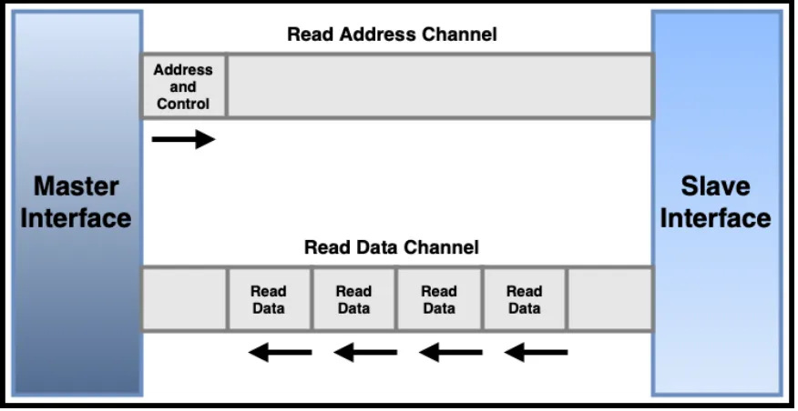
Figure 2.6 shows the channel architecture of the write transaction. In write transaction, the
process single starts by master sending address and control information to slave on the write
address channel followed by data on the write data channel. For burst write the write data channel
sends a WLAST at the end of the write data. The slave interface sends a write response back
to the master after accepting the write address and data. The write response from the slave to
indicates that the write transaction is complete. Figure 2.7 shows the channel architecture of
the read transaction. In read transaction, the process single starts by master sending address
and control information to slave via the read address channel. The slave interface sends a read
data corresponding to address back to the master after accepting the read address. The read
data is itself the read response from the slave that indicates the read transaction is complete. AXI
protocol can also connect multiple numbers of master and slave devices with a single interconnect
2.2 AXI Protocol 18
Figure 2.6: Write Transaction Channel Architecture
[image:37.612.88.526.440.666.2]2.3
SystemVerilog for Verification
In earlier days, the design of the ICs was not very sophisticated, which allowed designers to
verify their design using a self-developed test bench in Verilog-alone or with Verilog and C/C++.
As we proceed to the present era, the complexity of the design had increased considerably. The
effort of verification now dominates the design process, which led to the development of
var-ious verification tools and methodologies [47]. Verification languages such as Vera, Specman
e, and SystemVerilog are trendy. SystemVerilog is an object-oriented programming based
lan-guage that supports hardware verification. SystemVerilog provides the feature of using a layered
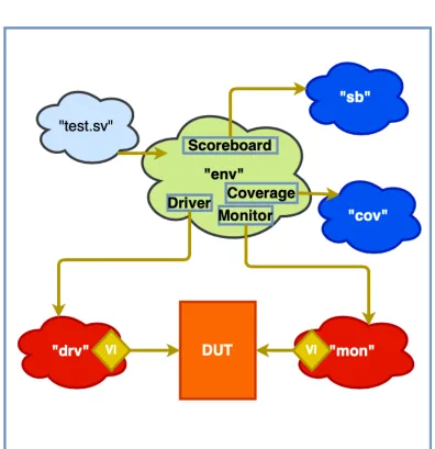
testbench with a constrained random stimulus [10]. Figure2.8shows a standard OOP testbench
architecture. It comprises of various components like program block, clocking block, interface,
packet, driver, environment, monitor, scoreboard, coverage and a top-level module that has the
DUT (Design under test) and interfaces connection. Table2.4 decribes various components of
OOP testbench.
Table 2.4: OOP Testbench Components [10]
Component Description
Program Block A program block separates the testcase and testbench entity,
so multiple numbers of testcases can use the same testbench.
It serves as a border between the RTL code and testbench.
Clocking Block A clocking block allows separating the functional behavior of
the design from its clocking behavior. It assembles signals
that are synchronous to a particular clock and makes their
2.3 SystemVerilog for Verification 20
Table 2.4: OOP Testbench Components [10]
Component Description
Interface In the purest form, an interface is simply a bundle of wire. It
is just like another module which can be instantiated and can
also instantiate other interfaces.
Driver The Drive is a design’s active entity. The driver component
has the logic that drives to DUT and sends data received from
the sequencer to the DUT. It continuously sends data to the
DUT and only stops when the sequencer stops sending data.
Monitor The Monitor stores, collects and monitors the transaction sent
from the DUT and the model. It also forwards the collected
transactions to the coverage checker.
Environment Agent, monitor, scoreboard, and coverage checkers are the
components of the environment, and the environment also
connects these components.
Scoreboard A scoreboard is used to check if the design is working as
expected. It compares the DUT output with the reference
Table 2.4: OOP Testbench Components [10]
Component Description
Coverage The percentage of the verification objectives met by design is
called coverage. Coverage metric is an important step to
evaluate the design. It also improves the quality of the
testbench. Coverage is classified into two types:
1. Code Coverage - Code coverage critiques on how good
the code is covered during the simulation. Code
coverage is an auxiliary add-on technology to the
language of Verilog. It is generated automatically by the
simulators.
2. Functional Coverage - The functional coverage is the
heart and soul of the RTL. It is user-defined and projects
how well the features have been applied to the design. It
checks the functionality of the design, covers corner
2.4 UVM for Verification 22
Table 2.4: OOP Testbench Components [10]
Component Description
Assertions Assertion describes the function of the design. Assertions can
be used to provide functional coverage and to flag the input
stimulus. If the assertion has described property that
mismatches the specification, the assertion fails and gives an
error. There are two types of assertions:
1. Immediate Assertion - Immediate Assertions are
expression-based and execute as a statement in
procedural blocks. There are used only in dynamic
simulation.
2. Concurrent Assertion - Concurrent Assertions are clock
based and execute concurrently like other blocks. There
are used in both static and dynamic simulation.
2.4
UVM for Verification
The inability of SystemVerilog to support metaprogramming, reflection facilities, and unlimited
macro capabilities started the development and rapid adoption of UVM (Universal Verification
Methodology) [48]. UVM is a well-established verification approach based on SystemVerilog
for IP and SoC [49]. Accellera released UVM version 1.0 in February 2011. With the use of
2.4 UVM for Verification 24
UVM proves to be a standardized method for SoC verification. The UVM methodology also
enables easy use, and reuse, of Transaction Level Modeling (TLM) interfaces and components.
It also offers to improve verification efficiency, data portability, and interoperability between tool
Architecture Overview
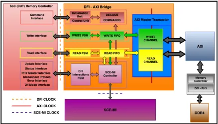
This chapter describes the design architecture of the DFI-AXI DDR4 Memory PHY Bridge.
Figure3.1shows the system-level architecture of the memory sub-system.
[image:44.612.87.525.386.636.2]3.1 SoC (DUT) Memory Controller 26
3.1
SoC (DUT) Memory Controller
The SoC Design under Test (DUT) includes a memory controller (MC) which provides a wide
range of address and data to the bridge module. It is responsible for sending the commands
signals, read signals, write signals, and other DFI interaction signals. It sends transfers signals
and requests to the DFI-AXI DDR4 Memory PHY Bridge module via the DFI. The next Section
3.2provides a detailed explanation of signals from the MC.
3.2
DFI
The DFI interface is a standard interface protocol. It defines signals and timing parameters
required to transfer data and information to/from the DRAM and between the memory controller
and PHY. Several electronic devices like smartphone, computers, network system use DFI. Both
designs for MC and PHY separately done by different companies; this causes the necessity for
DFI interface. DFI grants two different companies IP designs to interoperate with each other
[52].
The following are notable features of the DFI protocol:
• Supports low power mode
– Here the PHY may enter to an MC initiated low power state if PHY predicts that DFI
will be in an idle state for an extended period.
• Increases the sharpness of signal placement
– DFI write training and read training operations boost the accuracy of signal placement
at a higher speed in the DDR system.
– DFI allows changing the clock frequency of the MC and PHY without re-setting the entire system.
– It supports 1:1, 1:2, and 1:4 clock frequency ratio.
• Reduces power consumption and noise
– Data Bus Inversion reduces the number of transitions, which reduces power
con-sumption and noise.
3.2.1
Interface Group
The DFI specification is organized into the following interface groups, which consists of multiple
signals and their parameters [5]. Figure3.2shows the block diagram of Interface Signals.
3.2.1.1 Command Interface
The command interface manages signals needed to drive the address and command signals to the
DRAM. These signals have to maintain their timing relationship to the DRAM device through the
DFI. The command interface is made up of Command Address (CA) bus. The CA bus contains
address, command signals and other information like bank/row. CA signals include dfi_act_n,
dfi_address, dfi_bank, dfi_we_n, dfi_ras_n, dfi_cas_n, dfi_bg, and these commands are listed
in Table3.1 and Table3.2 defines its timing parameters. The encoded read or write command
3.2 DFI 28
Table 3.1: Command Interface Signals [5]
Signal From Description
dfi_act_n or
dfi_act_n_pN
MC DFI activate signal. This signal is used for encoding DRAM
commands. The following signals define all or a subset of the
command encoding: dfi_act_n, dfi_cas_n, dfi_ras_n,
dfi_we_n.
dfi_address or
dfi_address_pN
MC DFI address bus. These signals define the address
information. The PHY must preserve the bit ordering of the
dfi_address signals when it sends this data to the DRAM
devices. For DDR4 DRAMs, the dfi_address bus defines the
column address and a portion of the row address. DDR4
devices do not use the dfi_address bits [16:14] since DDR4
devices transmit the row address bits [16:14] on dfi_ras_n,
dfi_cas_n and dfi_we_n.
dfi_alert_n or
dfi_alert_n_aN
PHY CRC or parity error indicator. This signal is driven when a
CRC or command parity error is detected in the memory
system. The PHY is not required to distinguish between a
CRC and command parity error. The PHY holds the current
state until the PHY error input transitions to a new value; the
pulse width of the dfi_alert_n signal matches the pulse width
of the DRAM subsystem
dfi_bank or
dfi_bank_pN
MC DFI bank bus. These signals define the bank information. The
PHY must preserve the bit ordering of the dfi_bank signals
3.2 DFI 30
Table 3.1: Command Interface Signals [5]
Signal From Description
dfi_bg or
dfi_bg_pN
MC DFI bank group. This signal defines the bank group of a
command. The PHY must preserve the bit ordering of the
dfi_bg signals when it sends the DFI bank group data to the
DRAM devices.
dfi_cas_n or
dfi_cas_n_pN
MC DFI column address strobe. This signal is used for encoding
DRAM commands. The following signals define all or a
subset of the command encoding: dfi_act_n, dfi_cas_n,
dfi_ras_n, dfi_we_n.
dfi_cid or
dfi_cid_pN
MC DFI chip ID. This signal defines the chip ID. This signal is
required for 3D stacked solutions.
dfi_cke or
dfi_cke_pN
MC DFI clock enable. This signal defines the clock enable. The
MC must drive CKE signals in all phases. The PHY must be
able to accept a command on any and all phases for DFI
frequency ratio compliance.
dfi_cs or
dfi_cs_pN
MC DFI chip select. This signal defines the chip select. The
polarity of this signal is defined by the polarity of the
corresponding memory signal. For 3DS operation, also refer
Table 3.1: Command Interface Signals [5]
Signal From Description
dfi_dram_clk
_disable or
dfi_dram_clk
_disable_pN
MC DRAM clock disable. When active, this indicates to the PHY
that the clocks to the DRAM devices must be disabled such
that the clock signals hold a constant value. When the
dfi_dram_clk_disable signal is inactive, the DRAMs should
be clocked normally.
dfi_odt or
dfi_odt_pN
MC DFI on-die termination control bus. These signals define the
ODT. The MC must drive ODT signals in all phases. The
PHY must be able to accept a command on any and all phases
for DFI frequency ratio compliance.
dfi_parity_in or
dfi_parity_in_pN
MC Parity value. This signal has a one-to-one correspondence
with each DFI command and is valid for 1 cycle. This value
applies to the dfi_address, dfi_bank, dfi_bg, dfi_act_n,
dfi_cas_n, dfi_cid, dfi_ras_n and dfi_we_n signals. This signal
is relevant for only systems that support command parity.
’b0 = An even number of the parity value signals are
electrically high
’b1 = An odd number of the parity value signals are
electrically high
dfi_ras_n or
dfi_ras_n_pN
MC DFI row address strobe. This signal is used for encoding
DRAM commands. The following signals define all or a
subset of the command encoding: dfi_act_n, dfi_cas_n,
3.2 DFI 32
Table 3.1: Command Interface Signals [5]
Signal From Description
dfi_reset_n or
dfi_reset_n_pN
MC DFI reset bus. These signals define the RESET. The PHY
must preserve the bit ordering of the dfi_reset_n signals when
it sends the DFI chip ID data to the DRAM devices.
dfi_we_n or
dfi_we_n_pN
MC DFI write enable signal. This signal is used for encoding
DRAM commands. The following signals define all or a
subset of the command encoding: dfi_act_n, dfi_cas_n,
dfi_ras_n, dfi_we_n.
3.2.1.2 Write Data Interface
The write data interface is used to send write data across DFI that is it transfers signals from
the MC to the PHY [5]. The write data interface signals include dfi_wrdata_cs, dfi_wrdata_en,
dfi_wrdata, dfi_wrdata_mask, and these commands are listed in Table3.4and Table3.5lists its
parameters.
3.2.1.3 Read Data Interface
The read data interface is used to send read data across DFI that is it transfers signals from the
MC to the PHY [5]. The read data interface signals includes dfi_rddata_wN, dfi_rddata_en_pN,
dfi_rddata_cs_pN, dfi_rddata_dbi_wN, dfi_rddata_dnv_wN, dfi_rddata_valid_wN, and these
Table 3.2: Command Interface Timing Parameters [5]
Parameter Defined by
Description
t_cmd_lat MC Specifies the number of DFI clocks after the dfi_cs signal is
asserted until the associated CA signals are driven.
t_ctrl_delay PHY Specifies the number of DFI clock cycles from the time that
any command signal changes and when the change reaches the DRAM interface. If the DFI clock and the DRAM clock are not phasealigned, this timing parameter should be rounded up to the next integer value.
t_dram_clk_disable PHY Specifies the number of DFI clock cycles from the assertion of
the first phase of the dfi_dram_clk_disable_pN signal on the DFI until the clock to the DRAMs at the PHY-DRAM boundary maintains a low value.
NOTE: This parameter may be specified as a fixed value, or as a constant based on other fixed values in the system.
t_dram_clk_enable PHY Specifies the number of DFI clock cycles from the deassertion
of the first phase of the dfi_dram_clk_disable_pN signal on the DFI until the first valid rising edge of the clock to the DRAMs at the PHY-DRAM boundary. NOTE: This parameter may be specified as a fixed value, or as a constant based on other fixed values in the system.
t_parin_lat MC Specifies the number of DFI PHY clocks between when the
DFI command is asserted and when the associated dfi_parity_in signal is driven.
t_phy_paritylat PHY Specifies the maximum number of DFI clock cycles between
3.2 DFI 34
Table 3.4: Write Data Interface Signals [5]
Signal From Description
dfi_wrdata or dfi_wrdata_pN
MC Write data. These signals transfer write data from the MC to
the PHY tphy_wrdata cycles after the dfi_wrdata_en signal is asserted and continues transferring data for the number of cycles that the dfi_wrdata_en signal is asserted.
dfi_wrdata_cs or
dfi_wrdata_cs_pN
MC DFI write data chip select. The polarity of this signal is the
same as the polarity of the dfi_cs signal. This signal indicates the chip select that is accessed or targeted for associated write data.
dfi_wrdata_en or
dfi_wrdata_en_pN
MC Write data and data mask enable. This signal indicates to the
PHY that valid dfi_wrdata will be transmitted in tphy_wrdata cycles. Both tphy_wrlat and tphy_wrdata may be defined as zero. Ideally, there is a one-to-one correspondence between dfi_wrdata_en bits and PHY data slices. The dfi_wrdata_en [0] signal corresponds to the lowest segment of dfi_wrdata signals.
dfi_wrdata_mask or
dfi_wrdata_mask _pN
MC Write data byte mask. This bus is used for transferring either
the write data mask or the write DBI information, depending on system/DRAM settings. It uses the same timing as the dfi_wrdata signal. The polarity of this signal is defined by the polarity of the corresponding memory signal.
dfi_wrdata_mask [0] = Masking or DBI for the dfi_wrdata [7:0] signals
dfi_wrdata_mask [1] = Masking or DBI for the dfi_wrdata [15:8] signals, etc.
Table 3.5: Write Data Interface Timing Parameters [5]
Parameter Defined by
Description
t_phy_wrcsgap PHY This parameter specifies the minimum number of additional
DFI PHY clocks (or DFI PHY clock) cycles that are required between commands when changing the target physical rank that is driven on the dfi_wrdata_cs signal. This parameter must be supported in the MC transaction-to-transaction timing. The minimum assertion duration of dfi_wrdata_cs is determined by tphy_wrcsgap + dfirw_length.
t_phy_wrcslat PHY This parameter specifies the number of DFI PHY clock cycles
from the time that a write command is sent on the DFI command interface and when the associated dfi_wrdata_cs signal is asserted.
t_phy_wrdata PHY This parameter specifies the number of DFI PHY clock cycles
from the time that the dfi_wrdata_en signal is asserted and when the associated write data is driven on the dfi_wrdata signal. The parameter adjusts the relative time between enable and data transfer with no effect on performance. DFI 1.0 and DFI 2.0 MCs support a tphy_wrdata value of only 1. The MC should support a range of tphy_wrdata values. A PHY is designed to operate at a single tphy_wrdata value.
t_phy_wrlat PHY This parameter specifies the number of DFI PHY clock cycles
from the time that a write command is sent on the DFI command interface and when the dfi_wrdata_en signal is asserted.
t_wrdata_delay System This parameter specifies the number of DFI clocks from the
3.2 DFI 36
Table 3.6: Read Data Interface Signals [5]
Signal From Description
dfi_rddata or dfi_rddata_wN
PHY Read data bus. This bus transfers read data from the PHY to
the MC. Read data is expected to be received at the MC within tphy_rdlat cycles after the dfi_rddata_en signal is asserted. dfi_rddata_cs or
dfi_rddata_cs_pN
MC DFI read data chip select. The polarity of this signal is the
same as the polarity of the dfi_cs signal. This signal indicates which chip select is accessed or targeted for associated read data.
dfi_rddata_dbi or dfi_rddata_dbi_wN
PHY Read data DBI. This signal is sent with dfi_rddata bus
indicating DBI functionality. This signal is used by the MC only when phydbi_mode = 0. The polarity of this signal is defined by the polarity of the corresponding memory signal. When the dfi_rddata_dbi signal is used, it is sent with the dfi_rddata signal.
dfi_rddata_dnv or dfi_rddata_dnv_wN
PHY DFI data not valid. The timing is the same as for the
dfi_rddata_valid signal. The dfi_rddata_dnv [0] signal correlates to the dfi_rddata [7:0] signals, the dfi_rddata_dnv [1] signal correlates to the dfi_rddata [15:8] signals, etc. If the dfi_rddata bus is not a multiple of 8, the uppermost bit of the dfi_rddata_dnv signal corresponds to the most significant partial byte of data. This must be sent with the read data signal dfi_rddata when the dfi_rddata_valid signal is asserted. dfi_rddata_en or
dfi_rddata_en_pN
MC Read data enable. This signal indicates to the PHY that a read
operation to memory is underway and identifies the number of data words to be read. The dfi_rddata_en signal must be asserted trddata_en cycles after the assertion of a read command on the DFI command interface and remains valid for the duration of contiguous read data expected on the dfi_rddata bus. Ideally, there is a single dfi_rddata_en bit for each PHY data slice. The dfi_rddata_en [0] signal
corresponds to the lowest segment of dfi_rddata signals. dfi_rddata_valid or
dfi_rddata_valid _wN
PHY Read data valid indicator. Each bit of the dfi_rddata_valid
signal is asserted with the corresponding dfi_rddata for the number of cycles that data is being sent. The timing is the same as for the dfi_rddata bus. The width of the
Table 3.7: Read Data Interface Timing Parameters [5]
Parameter Defined by
Description
t_phy_rdcsgap PHY Specifies the minimum number of additional DFI PHY clocks
required between commands when changing the target physical rank driven on the dfi_rddata_cs signal. This parameter needs to be supported in the MC
transaction-to-transaction timing. The minimum assertion duration of dfi_rddata_cs is determined by tphy_rdcsgap + dfirw_length
t_phy_rdcslat PHY Specifies the number of DFI PHY clocks between when a read
command is sent on the DFI command interface and when the associated dfi_rddata_cs signal is asserted.
t_phy_rdlat PHY Specifies the maximum number of DFI PHY clock cycles
allowed from the assertion of the dfi_rddata_en signal to the assertion of each of the corresponding bits of the
dfi_rddata_valid signal.
t_rddata_en System Specifies the number of DFI PHY clock cycles from the
3.2 DFI 38
3.2.1.4 Update Interface
The update interface expedites commands transmitted through the DFI that require interference
or delay of signals [5]. The update interface signals are listed in Table3.8and Table3.9lists its
parameters.
Table 3.8: Update Interface Signals [5]
Signal From Description
dfi_ctrlupd_ack PHY MC-initiated update acknowledge. The dfi_ctrlupd_ack signal
is asserted to acknowledge an MC-initiated update request.
The PHY is not required to acknowledge this request. While
this signal is asserted, the DFI bus must remain in the idle
state except for transactions specifically associated with the
update process. If the PHY acknowledges the request, the
dfi_ctrlupd_ack signal must be asserted before tctrlupd_min
occurs and the dfi_ctrlupd_req signal de-asserts. If the PHY
ignores the request, the dfi_ctrlupd_ack signal must remain
de-asserted until the dfi_ctrlupd_req signal is de-asserted. The
dfi_ctrlupd_req signal is guaranteed to be asserted for at least
tctrlupd_min cycles. The dfi_ctrlupd_ack signal cannot be
asserted after tctrlupd_min, occurs, even if dfi_ctrlupd_req is
Table 3.8: Update Interface Signals [5]
Signal From Description
dfi_ctrlupd_req MC MC-initiated update request. The dfi_ctrlupd_req signal is
used with an MC-initiated update to indicate that the DFI will
be in the idle state for some time, in which case the PHY may
perform an update. The dfi_ctrlupd_req signal must be
asserted for a minimum of tctrlupd_min cycles and a
maximum of tctrlupd_max cycles. A dfi_ctrlupd_req signal
assertion is an invitation for the PHY to update and does not
require a response. The behavior of the dfi_ctrlupd_req signal
is dependent on the dfi_ctrlupd_ack signal:
If the update is acknowledged by the PHY, the dfi_ctrlupd_req
signal remains asserted as long as the dfi_ctrlupd_ack signal is
asserted, but dfi_ctrlupd_ack must de-assert before
tctrlupd_max expires. While dfi_ctrlupd_req is asserted, the
DFI bus remains in the idle state except for transactions
specifically associated with the update process.
If the update is not acknowledged, the dfi_ctrlupd_req signal
may de-assert at any time after tctrlupd_min occurs and
before tctrlupd_max expires.
The MC may de-assert the dfi_ctrlupd_req signal to
3.2 DFI 40
Table 3.8: Update Interface Signals [5]
Signal From Description
dfi_phyupd_ack MC PHY-initiated update acknowledge. The dfi_phyupd_ack
signal is used for a PHY-initiated update to indicate that the
DFI is idle and remains in the idle state until the
dfi_phyupd_req signal de-asserts. In most cases, the MC must
assert the dfi_phyupd_ack signal within tphyupd_resp cycles
of the dfi_phyupd_req signal; exceptions are granted when the
dfi_phymstr_req signal is also asserted. When the
dfi_phyupd_ack signal is asserted, it should remain asserted as
long as the dfi_phyupd_req signal remains asserted. The
dfi_phyupd_ack signal must de-assert upon the detection of
dfi_phyupd_req signal de-assertion. The dfi_phyupd_req
cannot be re-asserted prior to the de-assertion of
dfi_phyupd_ack for the previous transaction. The MC may
de-assert the dfi_phyupd_ack signal to disconnect the
Table 3.8: Update Interface Signals [5]
Signal From Description
dfi_phyupd_req PHY PHY-initiated update request. The dfi_phyupd_req signal is
used for a PHY-initiated update to indicate that the PHY
requires the DFI bus to be placed in an idle state and not send
control, read or write commands or data for a specified period
of time. The maximum time required is specified by the
tphyupd_typeX parameter associated with the
dfi_phyupd_type signal. Once asserted, the dfi_phyupd_req
signal must generally remain asserted until the request is
acknowledged by the assertion of the dfi_phyupd_ack signal
and the PHY’s internal update procedure has been completed.
Exceptions are granted if the dfi_ctrlupd_req,
3.2 DFI 42
Table 3.9: Update Interface Timing Parameters [5]
Parameter Defined by
Description
t_ctrlupd_interva MC Specifies the maximum number of DFI clock cycles that the
MC may wait between assertions of the dfi_ctrlupd_req signal.
t_ctrlupd_max MC Specifies the maximum number of DFI clock cycles that the
dfi_ctrlupd_req signal can assert.
t_ctrlupd_min MC Specifies the maximum number of DFI clock cycles after the
assertion of the dfi_phyupd_req signal to the assertion of the dfi_phyupd_ack signal. Exceptions are granted if
dfi_init_start, dfi_ctrlupd_req, or dfi_phymstr_req are active along with dfi_phyupd_req.
t_phyupd_type0 PHY Specifies the maximum number of DFI clock cycles that the
dfi_phyupd_req signal may remain asserted after the assertion of the dfi_phyupd_ack signal for dfi_phyupd_type = 0x0. The dfi_phyupd_req signal may de-assert at any cycle after the assertion of the dfi_phyupd_ack signal.
t_phyupd_type1 PHY Specifies the maximum number of DFI clock cycles that the
dfi_phyupd_req signal may remain asserted after the assertion of the dfi_phyupd_ack signal for dfi_phyupd_type = 0x1. The dfi_phyupd_req signal may de-assert at any cycle after the assertion of the dfi_phyupd_ack signal.
t_phyupd_type2 PHY Specifies the maximum number of DFI clock cycles that the
dfi_phyupd_req signal may remain asserted after the assertion of the dfi_phyupd_ack signal for dfi_phyupd_type = 0x2. The dfi_phyupd_req signal may de-assert at any cycle after the assertion of the dfi_phyupd_ack signal.
t_phyupd_type3 PHY Specifies the maximum number of DFI clock cycles that the
3.2.1.5 Status Interface
The status interface is responsible for dispatching status signals and information between the
PHY and MC. It initializes the PHY and also sets frequency values [5]. During regular operation,
the MC can request Frequency change with the status interface signals listed in Table3.10and
Table3.11lists its parameters.
Table 3.10: Status Interface Signals [5]
Signal From Description
dfi_freq_fsp MC DFI frequency set point. Indicates the operating frequency set
point for the system. This signal should change only at
initialization or during a DFI frequency change operation.
This signal is required for MCs and PHYs that support
mutiple frequency set points. This signal is required only for
the DRAMs that support FSP. This signal is optional for MCs
and PHYs that support only a single frequency. This signal is
valid when dfi_init_start is asserted during initialization and
3.2 DFI 44
Table 3.10: Status Interface Signals [5]
Signal From Description
dfi_freq_ratio MC DFI frequency ratio indicator. This signal defines the
frequency ratio for the system. This signal is required for
MCs and PHYs that support multiple frequency ratios and the
DFI frequency ratio protocol. This signal is optional for MCs
and PHYs that support only a single frequency ratio or do not
support the DFI frequency ratio protocol. This signal is only
valid when the dfi_init_start signal is asserted during
initialization and frequency changes.
’b00 = 1:1 MC:PHY frequency ratio (matched frequency)
’b01 = 1:2 MC:PHY frequency ratio
’b10 = 1:4 MC:PHY frequency ratio
’b11 = Reserved For memories that support a frequency ratio
only for data, the signal defines the frequency ratio for the
data interface.
dfi_frequency MC DFI frequency. This signal indicates the operating frequency
for the system. This signal should change only at
initialization, during a DFI frequency change operation, or
other times that the system defines. The number of supported
frequencies and the mapping of signal values to clock
frequencies are defined by the PHY, system, or both. This
Table 3.10: Status Interface Signals [5]
Signal From Description
dfi_init_complete PHY PHY initialization complete. The dfi_init_complete signal
indicates that the PHY is able to respond to any proper
stimulus on the DFI. All DFI signals that communicate
commands or status must be held at their default values until
the dfi_init_complete signal asserts. During a PHY
reinitialization request (such as a frequency change), this
signal is de-asserted. For a frequency change request, the
de-assertion of the dfi_init_complete signal acknowledges the
frequency change protocol. Once de-asserted, the signal
should only be re-asserted within tinit_complete cycles after
the dfi_init_start signal has de-asserted, and once the PHY has
3.2 DFI 46
Table 3.11: Status Interface Timing Parameters [5]
Parameter Defined by
Description
t_init_complete PHY During a frequency change operation, specifies the maximum
number of DFI clock cycles after the deassertion of the dfi_init_start signal to the reassertion of the dfi_init_complete signal.
t_init_complete_min PHY Minimum number of DFI clocks before dfi_init_complete can
be driven after a previous command.
t_init_start MC During a frequency change operation, this parameter specifies
the number of DFI clock cycles from the assertion of the dfi_init_start signal on the DFI until the PHY must respond by de-asserting the dfi_init_complete signal. If the
dfi_init_complete signal is not de-asserted within this time period, the PHY indicates that it can not support the frequency change at this time. In this case, the MC must abort the
request and release the dfi_init_start signal. After tinit_start expires, the PHY must not de-assert the dfi_init_complete signal. The MC
t_init_start_min PHY Minimum number of DFI clocks before dfi_init_start can be
3.2.1.6 Low Power Control Interface
The lower power control interface allows the PHY to enter power-saving mode [5].Table 3.12
shows the list of the Error Interface signals and Table3.13lists its parameters.
Table 3.12: Low Power Control Interface Signals [5]
Signal From Description
dfi_lp_ctrl_ack PHY Control low power acknowledge. The dfi_lp_ctrl_ack signal is
asserted to acknowledge the MC control low power
opportunity request. The PHY is not required to acknowledge
this request. If the PHY acknowledges the request, the
dfi_lp_ctrl_ack signal must be asserted within tlp_resp cycles
after the dfi_lp_ctrl_req signal assertion. Once asserted, this
signal remains asserted until the dfi_lp_ctrl_req signal
de-asserts. The signal de-asserts within tlp_ctrl_wakeup
cycles after the dfi_lp_ctrl_req signal de-asserts, indicating
that the PHY is able to resume normal operation. If the PHY
ignores the request, the dfi_lp_ctrl_ack signal must remain
de-asserted for the remainder of the low power mode
opportunity. The dfi_lp_ctrl_req signal is asserted for at least
3.2 DFI 48
Table 3.12: Low Power Control Interface Signals [5]
Signal From Description
dfi_lp_ctrl_req MC Control low power opportunity request. The dfi_lp_ctrl_req
signal is used by the MC to inform the PHY of an opportunity
to switch to a low power mode. When asserted, the MC
indicates that no more commands will be sent on the
command interface. The MC must assert a constant value on
the dfi_lp_ctrl_wakeup signal while this signal is asserted
before the request is acknowledged by the PHY through the
assertion of the dfi_lp_ctrl_ack signal or until tlp_resp cycles
have elapsed. The MC may increase the value of the
dfi_lp_ctrl_wakeup signal while the dfi_lp_ctrl_req signal is
asserted. Following the de-assertion of the dfi_lp_ctrl_req
signal, the PHY has tlp_ctrl_wakeup cycles to resume normal
Table 3.12: Low Power Control Interface Signals [5]
Signal From Description
dfi_lp_ctrl_wakeup MC Control low power wakeup time. The dfi_lp_ctrl_wakeup
signal indicates which one of the 16 wakeup times the MC is
requesting for the PHY. The signal is only valid when the
dfi_lp_ctrl_req signal is asserted. The dfi_lp_ctrl_wakeup
signal must remain constant until the dfi_lp_ctrl_ack signal is
asserted. Once the request has been acknowledged, the MC
may increase the dfi_lp_ctrl_wakeup signal, permitting the
PHY to enter a lower power state. The PHY is not required to
change power states in response to the wakeup time change.
The MC may not decrease this value once the request has
been acknowledged. The value of the dfi_lp_ctrl_wakeup
signal at the time that the dfi_lp_ctrl_req signal is deasserted
3.2 DFI 50
Table 3.12: Low Power Control Interface Signals [5]
![Figure 2.2: Decoding Row and Column Address Fields [1]](https://thumb-us.123doks.com/thumbv2/123dok_us/31075.2467/27.612.109.506.318.545/figure-decoding-row-column-address-fields.webp)
![Figure 2.4: State Diagram of DDR4 [3]](https://thumb-us.123doks.com/thumbv2/123dok_us/31075.2467/32.612.92.529.97.547/figure-state-diagram-of-ddr.webp)
![Table 2.3: DDR Command table [3, 5, 7, 9]](https://thumb-us.123doks.com/thumbv2/123dok_us/31075.2467/33.612.85.534.88.346/table-ddr-command-table.webp)
![Table 2.4: OOP Testbench Components [10]](https://thumb-us.123doks.com/thumbv2/123dok_us/31075.2467/39.612.95.506.120.544/table-oop-testbench-components.webp)
![Table 2.4: OOP Testbench Components [10]](https://thumb-us.123doks.com/thumbv2/123dok_us/31075.2467/40.612.98.515.118.540/table-oop-testbench-components.webp)
![Table 2.4: OOP Testbench Components [10]](https://thumb-us.123doks.com/thumbv2/123dok_us/31075.2467/41.612.100.509.116.491/table-oop-testbench-components.webp)
![Figure 3.2: Block diagram of DDR PHY Interface signals [5]](https://thumb-us.123doks.com/thumbv2/123dok_us/31075.2467/47.612.88.528.116.648/figure-block-diagram-ddr-phy-interface-signals.webp)