Rochester Institute of Technology
RIT Scholar Works
Theses Thesis/Dissertation Collections
2017
Wireless Interconnects for Intra-chip & Inter-chip
Transmission
Rounak Singh Narde
rn5949@rit.edu
Follow this and additional works at:http://scholarworks.rit.edu/theses
This Thesis is brought to you for free and open access by the Thesis/Dissertation Collections at RIT Scholar Works. It has been accepted for inclusion in Theses by an authorized administrator of RIT Scholar Works. For more information, please contactritscholarworks@rit.edu.
Recommended Citation
Wireless Interconnects for Intra-chip & Inter-chip Transmission
By
Rounak Singh Narde
A Thesis Submitted in Partial Fulfillment of the
requirements of the Degree of
MASTER OF SCIENCE
in
Electrical Engineering
Approved by:
Professor: ____________________________________
(Dr. Jayanti Venkataraman - Advisor)
Professor: ____________________________________
(Dr. Amlan Ganguly - Committee Member)
Professor: ____________________________________
(Dr. Panos P. Markopoulos - Committee Member)
Professor: ____________________________________
(Dr. Sohail A. Dianat – Department Head)
Department of Electrical and Microelectronic Engineering
Kate Gleason College of Engineering (KGCOE)
Rochester Institute of Technology
Rochester, New York
i
Acknowledgements
Most importantly I would like to thank my parents, sister and brother for always being
there for me. In difficult times, they always provided support, patience and encouragement. None
of this would be possibly without their endless support.
I thank Dr. Venkataraman for her patience, support, guidance and trust. She encouraged
me to do the best work. Her guidance took me towards the light of knowledge. She taught me
about engineering work ethics and responsibility. I would like to thank Dr. Ivan Puchades and Dr.
Lynn Fuller of Electrical and Microelectronic Engineering, KGCOE, RIT for providing silicon
wafers, and helping with the fabrication of antenna. I would also like to extend my thanks to Dr.
Amlan Ganguly and Dr. Panos Markopoulos for providing constructive feedbacks, and for their
precious time as committee members.
I would like to thank to the staff of Department of Electrical Engineering, KGCOE. Thanks
Jim for maintaining computers and softwares in lab, and introducing me to Ham Radio. Thanks
Ken for maintaining lab facilities, and ordering requirements from shops and websites. Thanks
Patty and Florence for helping out with office work. I thank Dr. M. Shahriar for productive
discussions. I would like to thank my colleagues Danita, Vincent, Santosh, Pramodh, Sachin,
Meenakshy and Pratheik for building positive and creative environment of learning and sharing in
lab. I extend my thanks to my friends Fatemeh, Upender, Prameet, Yogesh, Mordhwaj, Subhadeep,
ii
Abstract
With the emergence of Internet of Things and information revolution, the demand of high
performance computing systems is increasing. The copper interconnects inside the computing
chips have evolved into a sophisticated network of interconnects known as Network on Chip
(NoC) comprising of routers, switches, repeaters, just like computer networks. When network on
chip is implemented on a large scale like in Multicore Multichip (MCMC) systems for High
Performance Computing (HPC) systems, length of interconnects increases and so are the problems
like power dissipation, interconnect delays, clock synchronization and electrical noise. In this
thesis, wireless interconnects are chosen as the substitute for wired copper interconnects. Wireless
interconnects offer easy integration with CMOS fabrication and chip packaging. Using wireless
interconnects working at unlicensed mm-wave band (57-64GHz), high data rate of Gbps can be
achieved.
This thesis presents study of transmission between zigzag antennas as wireless
interconnects for Multichip multicores (MCMC) systems and 3D IC. For MCMC systems, a
four-chips 16-cores model is analyzed with only four wireless interconnects in three configurations with
different antenna orientations and locations. Return loss and transmission coefficients are
simulated in ANSYS HFSS. Moreover, wireless interconnects are designed, fabricated and tested
on a 6’’ silicon wafer with resistivity of 55Ω-cm using a basic standard CMOS process. Wireless
interconnect are designed to work at 30GHz using ANSYS HFSS. The fabricated antennas are
resonating around 20GHz with a return loss of less than -10dB. The transmission coefficients
between antenna pair within a 20mm x 20mm silicon die is found to be varying between -45dB to
iii
Furthermore, wireless interconnect approach is extended for 3D IC. Wireless interconnects
are implemented as zigzag antenna. This thesis extends the work of analyzing the wireless
interconnects in 3D IC with different configurations of antenna orientations and coolants. The
iv
Publications from the Present Work
1. M. S. Shamim, N. Mansoor, R. S. Narde, V. Kothandapani, A. Ganguly, and J. Venkataraman,
“A Wireless Interconnection Framework for Seamless Inter and Intra-Chip Communication in
Multichip Systems,” IEEE Trans. Comput., pp. 1–14, 2016.
2. R. S. Narde, J. Venkataraman and A. Ganguly, “Feasibility study of Transmission between
Wireless Interconnects in Multichip Multicore systems,” Proceedings IEEE International
Symposium on Antenna and Propagation and USNC-URSI Radio Science Meeting, San
v
Table of Contents
Acknowledgements ... i
Abstract ... ii
Publications from the Present Work ... iv
List of Figures ... vii
List of Tables ... xii
List of Abbreviations ... xiii
1. Introduction ... 1
1.1. Moore’s Laws & Dennard’s Scaling ... 1
1.2. Multicore systems ... 3
1.2.1. Multichip Multicore systems ... 4
1.2.2. Vertical Integration or 3D IC ... 5
1.3. Network on Chip ... 6
1.4. International Technology Roadmap for Semiconductors (ITRS) 2015... 9
1.5. Wireless Network on chip ... 10
1.6. Silicon ... 13
1.7. Review of Antenna on chip as Wireless Interconnects ... 15
1.8. Major Contribution ... 20
1.9. Organization of Present Work ... 20
2. Analysis of Planar antennas in various Si environments ... 22
2.1. Antennas in Free space ... 23
2.1.1. Linear monopole antenna ... 23
2.1.2. Linear Antenna with smaller GND ... 25
2.1.3. Zigzag monopole antenna ... 27
2.1.4. Zigzag monopole antenna with smaller GND ... 29
2.1.5. Circular loop antenna ... 31
2.2. On 5mmx5mm Si wafer without Ground plane at the bottom ... 33
2.2.1. Linear Monopole Antenna ... 33
2.2.2. Zigzag antenna ... 36
vi
2.3. On 5mmx5mm Si wafer with Ground plane at the bottom ... 40
2.3.1. Linear Antenna ... 41
2.3.2. Zigzag antenna ... 43
2.3.3. Circular loop antenna ... 45
3. Wireless Interconnects for Multichip-Multicore systems ... 48
3.1. Configuration 1 ... 50
3.2. Configuration 2 ... 52
3.3. Configuration 3 ... 55
4. Fabrication of zigzag antenna for MCMC system ... 58
4.1. Simulation design of antennas ... 58
4.1.1. Configuration 1 ... 59
4.1.2. Configuration 2 ... 60
4.1.3. Configuration 3 ... 62
4.2. Fabrication of antennas ... 63
4.3. Measurements & Results ... 64
4.3.1. Configuration 1 ... 67
4.3.2. Configuration 2 ... 68
4.3.3. Configuration 3 ... 69
5. Wireless Interconnects for 3D IC ... 72
5.1. Setup of 3D IC ... 72
5.2. Results ... 76
5.2.1. Return Loss Coolant #1 ... 77
5.2.2. Return Loss Coolant #2 ... 77
5.2.3. Transmission Coefficients – Antenna ‘a-1’ ... 78
5.2.4. Transmission Coefficients – Antenna b-1 ... 81
5.2.5. Transmission Coefficients – Antenna c-1 ... 84
5.2.6. Transmission Coefficients – Antenna d-1 ... 87
Conclusions ... 90
Future Work ... 92
vii
List of Figures
Figure 1-1: Reduction of gate length of transistor [3]. ... 1
Figure 1-2: Chronological progress towards multicore systems... 2
Figure 1-3: Eight cores on Intel Core i7-5960X Extreme Edition processor [6]. ... 3
Figure 1-4: Multicore systems. ... 4
Figure 1-5: Horizontal placed Multichip Multicore systems [7]. ... 5
Figure 1-6: Vertically placed Multichip Multicores systems [10]. ... 6
Figure 1-7: Wired interconnects. (a) chip cross-section view [11]; (b) 3D view [12]. ... 7
Figure 1-8: Block diagram representation of 2D mesh WNoC [17]. ... 11
Figure 1-9: Silicon wafers in a wafer boat [24]. ... 13
Figure 1-10: Antenna on chip [28] (a) Dipole (b) Zigzag (c) Meander (d) Loop. Axial length=2mm. ... 15
Figure 1-11: (a) Zigzag antenna on silicon wafer [29], (b) Cross-section of silicon wafer. ... 16
Figure 1-12: Monopole antenna with its return loss [30]. L=6mm and S=0.6mm. ... 16
Figure 1-13: CPW-fed zigzag antenna [31]. ... 17
Figure 1-14: Loop Antenna designed on silicon [33]. ... 18
Figure 1-15: Loop antenna designed with CPW feed for dual band operation (2.4/5.8GHz) [34]... 18
Figure 2-1: Linear monopole antenna. ... 23
Figure 2-2: Return loss of linear monopole antenna in free space. ... 24
Figure 2-3: Current density and radiation pattern in θ=90° planes (Azimuthal). ... 24
Figure 2-4: Radiation pattern in ϕ=0° and ϕ=90° planes (Elevation). ... 25
Figure 2-5: Linear monopole with small CPW ground in free space. ... 25
Figure 2-6: Return loss of antenna. At 60GHz, return loss = -11.85dB. ... 26
Figure 2-7: Current density and radiation pattern in θ=90° planes (Azimuthal). ... 26
Figure 2-8: Radiation pattern in ϕ=0° and ϕ=90° planes (Elevation). ... 27
viii
Figure 2-10: Return loss of zigzag monopole antenna. ... 28
Figure 2-11: Current density and radiation pattern in θ=90° planes (Azimuthal). ... 28
Figure 2-12: Radiation pattern in ϕ=0° and ϕ=90° planes (Elevation). ... 29
Figure 2-13: zigzag monopole antenna in free space. Trace width=5µm, Trace thickness=1µm. ... 29
Figure 2-14: Return loss of antenna. At 60GHz, return loss = -15.47dB. ... 30
Figure 2-15: Current density and radiation pattern in θ=90° planes(Azimuthal) ... 30
Figure 2-16: Radiation pattern in ϕ=0° and ϕ=90° planes (Elevation). ... 31
Figure 2-17: Circular loop antenna. ... 31
Figure 2-18: Return loss of antenna. ... 32
Figure 2-19: Current density and radiation pattern in θ=90° planes (Azimuthal). ... 32
Figure 2-20: Radiation pattern in ϕ=0° and ϕ=90° planes (Elevation). ... 33
Figure 2-21: Cross section view of setup (Not to scale). ... 33
Figure 2-22: Linear monopole in silicon dioxide over silicon. ... 34
Figure 2-23: Return loss of linear monopole antenna. ... 35
Figure 2-24: Current density and radiation pattern in θ=90° planes (Azimuthal). ... 35
Figure 2-25: Radiation pattern in ϕ=0° and ϕ=90° planes (Elevation). ... 36
Figure 2-26: Linear monopole in silicon dioxide over silicon. ... 36
Figure 2-27: Return loss of zigzag antenna. ... 37
Figure 2-28: Current density and radiation pattern in θ=90° planes (Azimuthal). ... 37
Figure 2-29: Radiation pattern in ϕ=0° and ϕ=90° planes (Elevation). ... 38
Figure 2-30: Circular loop antenna in silicon chip without ground. ... 38
Figure 2-31: Return loss of circular loop antenna. ... 39
Figure 2-32: Current density and radiation pattern in θ=90° planes (Azimuthal). ... 39
Figure 2-33: Radiation pattern in ϕ=0° and ϕ=90° planes (Elevation). ... 40
Figure 2-34: Cross section view of setup (Not to scale). ... 40
Figure 2-35: Linear monopole in silicon dioxide over silicon. ... 41
Figure 2-36: Return loss of antenna. ... 41
Figure 2-37: Current density and radiation pattern in θ=90° planes (Azimuthal). ... 42
Figure 2-38: Radiation pattern in ϕ=0° and ϕ=90° planes (Elevation). ... 42
ix
Figure 2-40: Return loss of zigzag monopole antenna in silicon dioxide over silicon
... 44
Figure 2-41: Current density and azimuthal radiation pattern of zigzag antenna. ... 44
Figure 2-42: Elevation plane radiation pattern of zigzag antenna. ... 45
Figure 2-43: Loop antenna in silicon dioxide over silicon. ... 45
Figure 2-44: Return loss of antenna. ... 46
Figure 2-45: Current density and radiation pattern in θ=90° planes (Azimuthal). ... 46
Figure 2-46: Radiation pattern in ϕ=0° and ϕ=90° planes (Elevation). ... 47
Figure 3-1: Cross-section of the model (Not to scale) ... 48
Figure 3-2: (a)MCMC system (Not to scale), C is core; (b) zigzag antenna with dimensions. ... 49
Figure 3-3: Top view of Configuration #1. ... 50
Figure 3-4: Return loss of four antennas... 51
Figure 3-5: Transmission coefficients. ... 51
Figure 3-6: Top view of configuration 2. Orientation of antenna is shown in inset. ... 52
Figure 3-7: Return loss of wireless interconnects. ... 53
Figure 3-8: Transmission coefficients of antennas. ... 53
Figure 3-9: Radiation pattern (Gain Total in HFSS) in azimuthal plane for configuration #2. (a) ANT 1, (b) ANT2, (c) ANT3, (d) ANT4. Note: the antenna orientation in the model (Figure3-6) and radiation pattern is inverted. Please read above plots carefully. ... 54
Figure 3-10: Top view of configuration #3. Inset: antenna orientation. ... 55
Figure 3-11: Return loss of antennas. ... 56
Figure 3-12: Transmission coefficients. ... 56
Figure 4-1: Cross-section of fabrication setup (Not to scale). ... 59
Figure 4-2: (a) Top view of configuration 1; (b) Zigzag antenna with GSG probe pads. ... 59
Figure 4-3: Return loss and transmission coefficients for configuration #1. ... 60
Figure 4-4: Curved CPW-fed zigzag antenna design with probe pads. ... 60
Figure 4-5: Top view of configuration #2... 61
x
Figure 4-7: Return loss and transmission coefficients for configuration #3. ... 62
Figure 4-8: Return loss and transmission coefficients for configuration #3. ... 62
Figure 4-9: Fabrication process. ... 63
Figure 4-10: (a) Fabricated antenna close up view, (b) Fabricated antenna for conf. 1... 64
Figure 4-11: Measurement instruments. ... 65
Figure 4-12: (a) Cascade ACP40-A probes, (b) Calibrating the system using standard (thru). ... 65
Figure 4-13: Probe placement on probe pad of an antenna. Another antenna is visible head-on. ... 66
Figure 4-14: Testing fabricated antenna using GSG probes on probe pads. ... 66
Figure 4-15: (a) Configuration 1, (b) Measured return loss of antennas for configuration 1. ... 67
Figure 4-16: Measured transmission coefficients for configuration 1. ... 67
Figure 4-17: Measured return loss of antennas for configuration 2... 68
Figure 4-18: Measured transmission coefficients for configuration 2. ... 68
Figure 4-19: Measured return loss of antennas for configuration 3... 69
Figure 4-20: Measured transmission coefficients for configuration 3. ... 69
Figure 4-21: Measured transmission coefficients for configuration #1 for frequencies 0.1-10GHz ... 71
Figure 5-1: Top view of configuration #1... 73
Figure 5-2: Top view of configuration #2... 73
Figure 5-3: (a) Full Side view, (b) close-up view of box in (a), (c) close up view (Not to scale). ... 74
Figure 5-4: Zigzag antenna with variables. 3D view of Zigzag antenna. ... 75
Figure 5-5: Return loss of all 16 antennas in setup with coolant #1. ... 77
Figure 5-6: Return loss for all 16 antennas in setup with coolant #2. ... 77
Figure 5-7: Transmission coefficients of antenna ‘a-1’ in conf. #1 coolant #1. ... 78
Figure 5-8: Transmission coefficients of antenna ‘a-1’ in conf. #2 coolant #1. ... 78
Figure 5-9: Transmission coefficients of antenna ‘a-1’ in conf. #1 coolant #2. ... 79
xi
Figure 5-11: Transmission coefficients of antenna ‘b-1’ in conf. #1 coolant #1. ... 81
Figure 5-12: Transmission coefficients of antenna ‘b-1’ in conf. #2 coolant #1. ... 81
Figure 5-13: Transmission coefficients of antenna ‘b-1’ in conf. #1 coolant #2. ... 82
Figure 5-14: Transmission coefficients of antenna ‘b-1’ in conf. #2 coolant #2. ... 82
Figure 5-15: Transmission coefficients of antenna ‘c-1’ in conf. #1 coolant #1. ... 84
Figure 5-16: Transmission coefficients of antenna ‘c-1’ in conf #2 coolant #1. ... 84
Figure 5-17: Transmission coefficients of antenna ‘c-1’ in conf. #1 coolant #2. ... 85
Figure 5-18: Transmission coefficients of antenna ‘c-1’ in conf. #2 coolant #2. ... 85
Figure 5-19: Transmission coefficients of antenna ‘d-1’ in conf. #1 coolant #1. ... 87
Figure 5-20: Transmission coefficients of antenna ‘d-1’ in conf. #2 coolant #1. ... 87
Figure 5-21: Transmission coefficients of antenna ‘d-1’ in conf. #1 coolant #2. ... 88
xii
List of Tables
Table 1: Predictions provided by ITRS 2015 [8]. ... 10
Table 2: Transmission coefficients of configuration #2 and #3 at 60 GHz ... 57
Table 3: Measured Transmission coefficient of fabricated configuration #1, #2 and #3 at 25 GHz ... 70
Table 4: Dimensions of antenna for coolant #1 (in µm). ... 76
Table 5: Dimensions of antenna for coolant #2 (in µm). ... 76
Table 6: Transmission coefficients for antenna a-1. ... 80
Table 7: Transmission coefficients for antenna b-1. ... 83
Table 8: Transmission coefficients for antenna c-1. ... 86
xiii
List of Abbreviations
AMC Artificial Magnetic Conductor
ANT Antenna
AoC Antenna-on-Chip
BCB Benzo-cyclo-Butene
BEOL Back End of Line
BOE Buffered Oxide Etch
CMOS Complementary Metal-Oxide-Semiconductor
CPW Co-planar Waveguide
EBG Electromagnetic Band-Gap
FCC Federal Communications Commission
FEOL Front End of Line
GND Ground
GSG Ground-Signal-Ground
HFSS High Frequency Structure Simulator
HPC High Performance Computing
IC Integrated Circuit
IoE Internet of Everything
IoT Internet of Things
ITRS International Technology Roadmap for Semiconductors
MCMC Multichip Multicores
MIMO Multiple Input Multiple Output
xiv
NoC Network on Chip
PCB Printed Circuit Board
PEC Perfect Electric Boundary
PNA Programmable Network Analyzer
RFIC Radio Frequency Integrated Circuit
RIT Rochester Institute of Technology
SMFL Semiconductor and Microelectronics Fabrication Laboratory
SOI Silicon On Insulator
TSV Through Silicon Via
UWB Ultra-Wide Band
WLAN Wireless Local Area Network
1
1.
Introduction
1.1.
Moore’s Laws & Dennard’s Scaling
In 1965, Gordon Moore, one of the founder of Intel, reported prediction that the number of
components in a chip will be doubled every two years [1]. This statement is known as Moore’s
law. Over the years, the size of MOSFETs has become smaller and smaller, so as to keep up with
the trend of doubling number of transistors in a chip. Now, it has become so small that it is reaching
atomic limit [2], [3]. This means that the Moore’s law is on the verge of collapse. Researchers are
implementing a 3D IC arrangement, which is discussed in later section, to keep up the Moore’s
[image:17.612.153.455.354.602.2]trend of doubling the number of components every 2 years.
Figure 1-1: Reduction of gate length of transistor [3].
Talking about decades old trends, there was one more which failed in 2004 [2]. It was
2
paper [4] stating a relationship between the parameters of MOSFET. The parameter includes the
dimension, voltage, current, power, operating frequency. Dennard’s paper emerged an industry
standard for MOSFET scaling for nearly three decades [5]. It provided a way to increase the
operating frequency and at the same time reducing the size of transistors. Till 2004, the Dennard’s
scaling worked good. It showed a way to engineers to increase the operating frequency of transistor
till 3 to 4 GHz. That was it, and it collapsed due to unbearable heat density, and limits to switching
voltage. The collapse of Dennard’s scaling forced the semiconductor industry to move from single
core to multicore systems in order to keep up with the Moore’s trend [2].
Figure 1-2: Chronological progress towards multicore systems.
Multicore processors work on the concept of distributed or parallel processing. A process
is distributed in between multiple computing units or cores. The concept of multicore systems &
parallel processing are alternatives to overcome the collapse of Dennard’s scaling, however, it is
limited by the communication between cores [2]. Since, the cores require to communicate or
exchange data with other cores for processing data in parallel, it is a must to have a high speed
3
1.2.
Multicore systems
Since, the collapse of Dennard’s scaling the performance of computing systems are
improved not by increasing the operating frequency, but by dividing a processor into multiple
independent processing units known as cores. In 2004, Intel was the first to move towards
multicore systems in a processor [2]. The layout (Figure 1-3) of the processor shows eight similar
[image:19.612.196.417.247.504.2]blocks of independent cores on a single silicon die.
Figure 1-3: Eight cores on Intel Core i7-5960X Extreme Edition processor [6].
Multicores systems can be fabricated in two ways: on a Single silicon wafer, or on multiple
silicon wafers. Fabricating multiple cores on a single standard sized silicon wafer has a problem.
If any core in the middle of the wafer gets defective it cannot be used. The whole wafer becomes
defective. This results in lower yield, moreover the single wafer design is expensive to maintain.
4
Figure 1-4: Multicore systems.
On the other hand, fabricating multiple cores of a processor on multiple silicon wafers has
relatively high yields, and more flexible placing chips on Printed circuit board (PCB). Therefore,
the multichip multicore (MCMC) design is popular among processor architects. Furthermore,
multichip multicore design can be divided in two types depending on integration of multiple chips:
Horizontal integration and Vertical integration. The horizontally integrated multicore systems are
commonly called Multichip Multicore (MCMC) system. Of late, there has been great interest seen
in designing vertical integrated multicore systems, also known as 3D IC, which are discussed in
later section.
1.2.1. Multichip Multicore systems
It is abbreviated as MCMC systems. It has multiple cores distributed in multiple chips on
a interposer or PCB horizontally. This type of systems is mostly used in High Performance
Computing (HPC) centers like datacenters, weather forecasting centers, etc. An example of
5
sockets. Furthermore, a socket is divided into multiple cores. Each core has a separate computing
unit along with its cache memory. Each core in a socket is connected with wired copper
interconnects. Each socket is connected using metal interconnects. Generally, HPC systems house
[image:21.612.78.533.197.422.2]more than 10 such processors working in parallel.
Figure 1-5: Horizontal placed Multichip Multicore systems [7].
As number of sockets increase, the system demands more space to distribute the chips
horizontally. This in turn requires longer metal interconnects for connections which results in delay
and ohmic losses. To maintain dissipating signal requires additional circuitry such as repeaters.
One emerging solution to this problem is to integrate cores vertically.
1.2.2. Vertical Integration or 3D IC
As mentioned in ITRS [8] that in big cities when the real estate on ground is fully used,
people started building in “vertical dimension”. Similar strategy is adopted by engineers in 3D IC.
Recently flash memory manufacturers have demonstrated 3D memory units [9]. In the coming
6
In a 3D IC, active silicon layers are placed one over other. In this way, a new dimension of
increasing the performance of processor is devised. This 3D configuration, however, complicates
the communication interfaces. A new type of metal interconnect is used which transfers signals
between cores through the bulk silicon layer, therefore known as Through-Silicon Via or TSV or
3D via. A 3D IC is shown in Figure 1-6 with three active silicon layers as Tier 1,2 and 3. TSV can
also be seen in the Figure 1-6 which are connected silicon layers.
Figure 1-6: Vertically placed Multichip Multicores systems [10].
1.3.
Network on Chip
The digital circuitry, mostly MOSFET, are fabricated on silicon wafer using variety of
standard process technologies. This design is called a Front End of Line (FEOL). The front end
layer is nothing but two dimensional placements of MOSFET on a silicon wafer. The front end
does not include connections between different MOSFETs or other devices. A metal wire or
interconnect is fabricated to support the transfer of power, signal and data. Metal used to fabricate
interconnects are Copper. Metal interconnect are designed in Back End of Line (BEOL) which is
7
interconnect does not only provide connections between MOSFET in FEOL, but also connects to
the outer package pins using a solder bump. The lead solder bump can be seen in Figure 1-7(a).
[image:23.612.72.542.138.455.2]
(a) (b)
Figure 1-7: Wired interconnects. (a) chip cross-section view [11]; (b) 3D view [12].
Till the start of 21st century, each device on chip were connected with separate
interconnects. This point-to-point communication made interconnect design bulky and
cumbersome to fabricate. Designing interconnects quickly became toil because connection should
be made between millions, if not billions, of transistors in different layers. Moreover, the scaling
of interconnects with smaller technology node was problematic [13] due to increasing power
consumption [14], delay, electro-mitigation, electrical noise and clock synchronization [15]. A
researcher from Intel noted in 1995 that the efficient implementation of high performance
computing systems depends on the metal interconnects [13]. Considering limitations of metal
8
interconnects, a new interconnect system was proposed in 2002 which implemented networks of
interconnects based on computer networking [15]. Switches, routers, hubs and other networking
devices were designed on chip to support the Network-on-chips (NoC). Moreover, different
networking algorithms like mesh, bus, et al. based on large computer networks were implemented
to improve the interconnect performance. It is really a smart way to overcome interconnect
problems in a computer chip. It is still used in today’s commercial computing systems.
As the transistors become smaller and smaller with technology nodes, the interconnects
become thinner and thinner, consequently more resistive which causes heat dissipation. It has been
studied that the metal interconnects alone consume 30-60% of the dynamic power of the chip [2].
Long copper interconnects in multi-hop networks for data transfer results in high latency and
power loss [16]. To make the signal go long distances, repeaters or buffers are introduced which
further increases the delay between the interconnects. Furthermore, it is noted that in a chip, the
repeaters take more space than the computing devices [2].
To cope with power consumption by metal interconnects, designers have created
multi-width multi-layer interconnects. In process technology of 22nm, number of interconnect layers can
go up to 16 of different width [2]. Still, interconnects consume significant amount of power and
takes up considerable space in a sub-micron world. Therefore, it is required to research new
techniques for improving current infrastructure of interconnects in high performance multicore
systems. Researchers have proposed Wireless Network on Chip (WNoC), which is discussed in
9
1.4.
International Technology Roadmap for Semiconductors (ITRS) 2015
ITRS [8] is a set of guidelines consist of future developments and predictions about
semiconductor devices written by the experts from semiconductor industries across Europe, Japan,
Korea, Taiwan, and USA. The main focus of the ITRS 2.0 is Internet of Everything (IoE), or
otherwise known as Internet of Things (IoT). “IoE is nothing more than a distributed computer
system” [8] with memories located remotely. This leads to improvement in technologies related to
IoT which includes datacenters, communications, et al.
According to ITRS predictions, the demand for data processing is going to increase
tremendously by 2029. It is predicted that number of cores on one socket of datacenter will increase
30 times. Moreover, the memory storage will increase to 4000 times. The predicted augmentation
of computing systems will result to another projection of power consumption by future data giants
by 2.5 times increment. A table from the ITRS summary is shown in Table 1. According to [2] in
2011, the datacenters in USA consumed 2.2% of its total power generated. Current consumption
of power is already substantial. It will be difficult to cope up with increase in power consumption.
In this way, a new efficient and robust communication technology is needed to take care
of the future demands. Moreover, it has been stated in ITRS that the wired interconnects inside a
chip and communication interfaces between chips are bulky, increases latency when interconnects
are long, and increases operating temperature due to heat generated. Therefore, research for
10
Table 1: Predictions provided by ITRS 2015 [8].
1.5.
Wireless Network on chip
When the traditional NoC grows too large into a multi-hop link between two distant
locations, the limitations of metal interconnect becomes significant [17]. So, the traditional NoC
limits the on chip communication system design. As discussed in [13], the performance of
computing systems is limited by the metal interconnects. Wireless Network on Chip (WNoC) can
help to cope with the barriers in NoC. It has already been demonstrated using modelling and
simulations in [17], [18], [19] and [20] that WNoC improves the throughput and decrease the
energy consumption. Moreover, the routing algorithm used by the Wireless network on chip can
11
Figure 1-8: Block diagram representation of 2D mesh WNoC [17].
As shown in previous sections, collapsing Moore’s law and predictions by ITRS 2015 must
be considered in order to keep up with increasing demand for optimum and faster processing.
Photonics is another technology with advantages of low latency, high bandwidth which may
overcome the limitations of wired metal interconnects. However, Photonics integrated circuits has
to overcome the technological challenges of size reduction of optical components, and
manufacturing challenges to be viable for mass production. Currently the cost of fabricating is
high, and size of interconnects is large for commercial purpose. Silicon Photonics is currently at
an early stage where silicon electronics was in 1970 [21], [22].
According to Shannon–Hartley theorem, high speed data communications requires large
bandwidth. The unlicensed bandwidth of present high speed communication system is limited
according to band of 2.4 GHz or 5 GHz. Therefore, Federal Communications Commission (FCC)
12
This millimeter wave frequency band is commonly known as 60 GHz frequency band, since it is
centered around 60 GHz. The allocation made possible the realization of ultrahigh speed
communication systems. Moreover, the range of frequency helps design an antenna of very small
size (of micrometer dimensions) which is feasible for fabricating antenna on chip. In this way,
small wireless interconnects for WNoC can be implemented on semiconductor devices.
One more advantage of Wireless is obviously it is wireless. No wired interconnect is
required to transfer data from one chip to another. The fact that different data transfer protocols
are used at different interfaces, so data is converted into specific blocks corresponding to interfaces
which increase the delay and complexity. But with direct wireless links, complexity and delay will
reduce. This will increase the performance, and save chip space of CMOS devices.
Since, here, the transmission of 60 GHz band is used for short distance with a maximum
of 10 meters. Moreover, the 60 GHz band cannot even penetrate concrete walls. It has a high
attenuation rate in atmosphere. All above mentioned reasons is going to decrease the chances of
Spoofing (unauthorized access using wireless protocols), thereby increasing security. Another
advantage is the fabrication process of antenna on chip (AoC) is compatible with existing CMOS
technology. The antennas are easily fabricated using standard process technology used by the
semiconductor industry today.
Since the beginning of wireless communication, it has touched the life of everyone. Most
of the communication systems of the world depends on wireless technology. This means that the
wireless technology has become mature and stable. There has been many research already done.
13
beam steering, etc. are yet to be implemented on chip. This creates opportunity for researchers to
investigate the ways to connect chips wirelessly.
1.6.
Silicon
It is the most dominated substrate for designing microelectronics circuitry due to its unique
properties. Some of the properties are described below.
[image:29.612.206.404.228.425.2]
Figure 1-9: Silicon wafers in a wafer boat [24].
1. Abundantly available: One of the simplest reason to use silicon for semiconductor industry is because silicon is available to us as silica (sand) in abundance. Silicon makes
up more than 25% of the earth’s crust. There are standard metallurgical processes devised,
over the years, to obtain metallurgical-grade silicon from sand (silica). Using Czochralski
process, metallurgical-grade silicon is converted into electronics-grade silicon. To get
ultra-pure silicon crystals, Float zone method is implemented following the Czochralski
process.
2. High quality native-oxide formation: Silicon forms a native oxide (SiO2) by reacting
14
This property outshines silicon in the list as SiO2 acts as high quality electrical insulator.
The dielectric strength of thin layer (≈1µm) SiO2 on silicon varies from 5-8 MV/cm.
Therefore, SiO2 is used as insulation in fabrication process. It can also be used to mask a
part of wafer while treating another part. One more significance is the silicon-dioxide over
silicon can be selectively etched using a Buffered Oxide Etch (BOE) solution, means the
underneath silicon is not etched.
3. Doping can easily change the conductivity: The different conductivity is required depending on different applications, so a good microelectronics material should be able to
change its electrical properties without much hassle. Silicon can be doped with impurity
like Boron, Phosphorous, Arsenic to change the conductivity of the wafer. Boron impurity
acts as acceptor impurity and used to make hole enriched or p-type silicon wafer.
Phosphorous and Arsenic act as donor impurity which makes electron enriched or n-type
silicon wafer.
4. Chemically resist – Due to crystalline structure of silicon, it is chemically inert. The durability of silicon microelectronics is more than other semiconductor materials can offer.
As seen above, silicon is most appropriate material for semiconductor industry. However,
when it comes to microwave or millimeter wave applications, silicon is a hostile material.
Following are some of the reasons:
1. High dielectric constant – Silicon has a high dielectric constant (εr) of 11.7 [24]. This
extreme property of silicon makes it a tough material to implement a high frequency circuit
or antenna. Because of high dielectric constant, most of the radiation of antennas goes into
15
2. Lossy due to high conductivity – Electronics grade silicon is doped, so it is conductive (generally ρ of Si wafers varies from 5mΩ-cm-30Ω-cm [25], so σ varies from 0.03S/cm to
200S/cm), therefore acts as a lossy medium. Note: High and ultra-high resistivity silicon
[24] can be used for RFIC working at GHz and THz. High resistivity Si wafers are
expensive because requires additional process of filtration of impurity (Float Zone
process).
1.7.
Review of Antenna on chip as Wireless Interconnects
The research on Antenna on Chip (AoC) is going on for more than two decades now. One
of the earliest implementation was planar microstrip antenna array [26] in 1986. It was
implemented with a 95GHz oscillator circuit on a very high resistivity substrate (ρ=10000Ω-cm).
Later in 2000, AoC was implemented with an aim to demonstrate the idea of wireless clock
distribution in digital integrated circuits [27].
Figure 1-10: Antenna on chip [27] (a) Dipole (b) Zigzag (c) Meander (d) Loop. Axial length=2mm.
Another modified form of zigzag antenna shown in Figure 1-10 (b) is provided in [28].
Figure 1-11 shows the design of dipole antenna and substrate cross-section. This antenna showed
16
Figure 1-11: (a) Zigzag antenna on silicon wafer [28], (b) Cross-section of silicon wafer.
Above shown dipole antenna is modified into a monopole [29] with long sleeves for ground
shown in Figure 1-12. This antenna was tested at frequency centered around 6 GHz. Despite little
change in radiation pattern of monopole, its performance is similar to the dipole. Moreover,
monopole antenna takes less space than dipole antenna shown above.
Figure 1-12: Monopole antenna with its return loss [29]. L=6mm and S=0.6mm.
All aforementioned antennas do not include feed, but excited by GSG probes. A zigzag
antenna with co-planar waveguide (CPW) feed was designed in [30]. It is shown in Figure 1-13.
17
be easily fabricated on a single layer without a bottom ground plane, unlike microstrip feed. The
zigzag antenna is optimized and simulated to work at 60GHz. It was simulated in ANSYS
[image:33.612.127.481.162.413.2]HFSS[31].
Figure 1-13: CPW-fed zigzag antenna [30].
A loop antenna is also designed on silicon wafer using CMOS technology in [32]. The
antenna is shown in Figure 1-14. The antenna is simulated to work at 60GHz. The loop antenna
uses multiple-layer fabrication. One half was fabricated at the top layer of BEOL of chip, and
18
Figure 1-14: Loop Antenna designed on silicon [32].
In [33], it is shown that the rectangular loop antenna has low profile, easy to fabricate, and
dual band characteristic. It is designed for WLAN applications with an omnidirectional pattern. A
CPW-fed loop antenna based on [33] is proposed in later chapter to take advantage of dual band
or it can be modified for a UWB antenna which is required for 60GHz frequency band.
Figure 1-15: Loop antenna designed with CPW feed for dual band operation (2.4/5.8GHz) [33].
Moreover, directional antennas such as log-periodic antenna [34]; Yagi antenna [37], [38],
[37]; dielectric resonator [38] have been fabricated on chip. It is to be noted that the AoC
19
can be increased by using different techniques like air cavity, micromachining, et al. and using
substrates like Silicon on Insulator (SoI), SiGe, GaAs; and different process technology like
BiCMOS-9MW, layer of Benzo-cyclo-Butene (BCB) polymer, etc. Performance Evaluation of
various antennas on chip can be found in publications [39], [40], [41] and [42]. In this work, only
monopole zigzag antenna is implemented for WNoC in MCMC systems and 3D IC.
To solve the problem of wired network on chip, wireless network on chip is implemented.
One of the main component of WNoC is antenna on chip known as wireless interconnect. The
earliest implementation of wireless interconnects (or AoC) for WNoC is implemented in [43] using
capacitive and inductive coupling.
Wireless network on chip implemented in [18] using log periodic antennas which are
directional antennas. Another implementation of Carbon nanotubes directional antenna for WNoC
is shown in [44]. A simulation-based study on Wireless Network on chip performed using zigzag
antenna is in [19], which is extended in chapter 3. Fabrication of zigzag antennas are performed in
chapter 5.
For WNoC in 3D IC, meander dipole antenna of length 2.4mm are simulated as wireless
interconnects [45]. This analysis is performed in X-band (8-12GHz) region. Another simulation
study of wireless interconnects using zigzag antennas at 60GHz is shown in [30]. The study uses
a setup of multiple-tier 3D IC with micro-fluidic coolant channels for thermal management. In this
thesis, work of [30] is extended by using two different antenna orientation and two different
20
1.8.
Major Contributions
Due to increasing demand of high performance computing and IoT, it is required to come
up with a new and efficient way of decreasing the delays and power consumptions. So Wireless
Network on chip is proposed. One of the main part of it is wireless interconnects. In this work,
study of transmission between wireless interconnect is performed. The simulations are performed
in ANSYS Electronics suite (HFSS) [31].
a) Planar antennas as wireless interconnect is analyzed on silicon with and without ground plane
with respect to distortions in the radiation pattern.
b) Transmission study of wireless interconnect in multichip multicore system using the zigzag
antenna as the radiator.
c) Zigzag antennas have been fabricated on silicon for 30GHz at RIT’s Semiconductor
Microsystems Fabrication Laboratory (SMFL). Using the Cascade probe station and Agilent
PNA., the return loss and the transmission between on-chip antennas have been measured.
d) A 3D IC with cooling channels has been analyzed for two different wireless interconnects
configurations and two different coolants to study the feasibility of transmission between the
silicon active layers.
1.9.
Organization of Present Work
The thesis presents work related to wireless interconnect. It does not consist of details on
Wireless Network on chip networking algorithms. The thesis is divided into chapters which are
21
Analysis of Planar Antenna on Silicon: This chapter details characteristics of antennas such as linear monopole, zigzag antennas and circular loop antenna in different setups which include
silicon with and without perfect electrical boundary (PEC).
Wireless Interconnects for MCMC systems: This chapter collects all different models simulated for zigzag antennas as wireless interconnects in MCMC systems. The positions of
wireless interconnects are varied to analyze the transmission coefficients between wireless
interconnects.
Fabrication of Wireless Interconnects on silicon: This chapter discusses the design procedure and results of zigzag antennas which are fabricated on silicon wafer at
Semiconductor & Microelectronics Fabrication Lab at Rochester Institute of Technology,
Rochester, NY.
Wireless Interconnects for 3D IC: This chapter collects HFSS [31] simulation results performed using zigzag antennas in a 3D IC structure. To cope up with the heat generated in
3D IC microchannels are designed. Analysis of antennas with two different configurations and
two different coolants is performed. At last, a comparison between transmission coefficients
22
2.
Analysis of Planar antennas in various Si environments
To understand the antennas on chip, it is important to simulate single antennas on different
arrangement of silicon. The aim of the chapter is to provide results and observations of antennas
behavior when placed on a Si wafer. The results provided in the report are current density, return
loss and radiation pattern. The radiation pattern of the antenna is plotted. Furthermore, the
comparison of radiation pattern for antennas in different environments is performed. This section
presents results of simulations performed in following setups:
In Free space.
On 5mmx5mm Si wafer without Ground plane.
On 5mmx5mm Si wafer with Ground plane.
All configuration has one antenna at a time. Three different Al antennas structures such as
Linear monopole, Zig-Zag monopole and Circular Loop antennas are simulated with Co-planar
waveguide(CPW) feed. The antenna is designed using ANSYS Electronics Desktop(HFSS)[31] to
resonant at 60GHz. The CPW feed is fed using a lumped port in simulation software. For
simulating a frequency sweep like from 0.25GHz to 80GHz, interpolating sweep is used rather
than fast sweep. Fast sweep is used for small frequency interval and less mesh elements. For more
details, on frequency sweep please refer to ANSYS Help. As per instructions from ANSYS Help,
it is required to place the radiation boundary at least /4 distance from the radiating sources.
Simulation results like current density, return loss, radiation pattern are discussed. We will
start with the simplest antennas of three, the Linear monopole antenna, and the simplest
23
2.1.
Antennas in Free space
To design and verify the antenna structures and results, first antennas are designed in free
space. This is only a hypothetical setup since the antennas are planar, they require a support
substrate to work. Free space setup is simulated only to compare with the results of other
configuration.
2.1.1. Linear monopole antenna
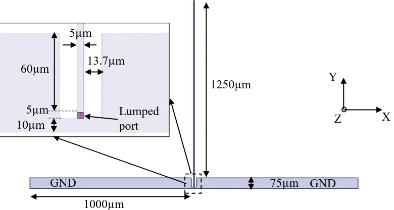
A planar linear monopole antenna is designed with large ground to operate at 60GHz. The
length of the monopole is 0/4; at 60GHz 0/4=1250µm. It is fed by a Co-planar waveguide
[image:39.612.110.500.351.559.2](CPW). The CPW is excited by using a lumped port in ANSYS HFSS.
Figure 2-1: Linear monopole antenna.
The return loss is shown in Figure 2-2. It shows that the antenna is resonating with a return
loss of -12dB at 60GHz.
1250µm
1000µm
Y
X Z
75µm 13.7µm
10µm 60µm
5µm
5µm
GND GND
24
Figure 2-2: Return loss of linear monopole antenna in free space.
Current density in Figure 2-3 is showing that the current is flowing through the monopole,
moreover the current distribution is as expected for monopole that is quarter wavelength.
Moreover, the radiation pattern is shown in azimuthal plane i.e. the plane of the antenna. The
radiation pattern in azimuthal plane is similar to the monopole wire antenna in free space.
Figure 2-3: Current density and radiation pattern in θ=90° planes (Azimuthal).
Next, radiation pattern in elevation plane is shown in Figure 2-4. It can be seen that the
radiation pattern is like donut shape just like a monopole wire antenna. However, the gain is
0.98dBi which is less than a monopole antenna in free space.
X
25
Figure 2-4: Radiation pattern in ϕ=0° and ϕ=90° planes (Elevation).
2.1.2. Linear Antenna with smaller GND
The required antenna for fabricating on chip should be low-profile, easy to fabricate,
therefore the size of ground plane of CPW feed is reduced just like monopole antenna with long
sleeves shown in [29]. After reducing the bottom CPW feed’s GND of Linear monopole of
previous section, the resonant frequency increases a lot. To make the monopole resonant on
60GHz, it is required to increase the length of monopole. The new length of monopole which is
resonating at 60GHz is 1680µm.
Figure 2-5: Linear monopole with small CPW ground in free space. Z
X Y
Z
Y X
Y
X Z
1680µm
100µm
26
Return loss plot is shown in Figure 2-6. It can be seen that at 60GHz the antenna is
resonating at 60GHz with a return loss of -11.85dB.
Figure 2-6: Return loss of antenna. At 60GHz, return loss = -11.85dB.
The current density and radiation pattern(azimuthal plane) plot are shown in Figure 2-7.
The current distribution of the antenna shows that the antenna is quarter-wave long. The radiation
pattern in azimuthal plane shows that the antenna still has overall donut shape with little
abnormality.
Figure 2-7: Current density and radiation pattern in θ=90° planes (Azimuthal).
The elevation plane radiation pattern is shown in Figure 2-8.
X
27
Figure 2-8: Radiation pattern in ϕ=0° and ϕ=90° planes (Elevation).
2.1.3. Zigzag monopole antenna
To save space in axial direction, low-profile zigzag antenna is designed which acts similar
to linear monopole antenna [46]. The calculation of actual length of zigzag antenna is shown. It
can be seen that the actual length of zigzag monopole antenna shown below is around 0/4 at
60GHz.
𝐿𝑎𝑐𝑡𝑢𝑎𝑙 =
𝐿𝑎𝑥𝑖𝑎𝑙
sin (𝜃2)+ 50𝜇𝑚 =
703µm
sin (30°2 )+ 50𝜇𝑚 = 2766𝜇𝑚
Figure 2-9: Zigzag monopole antenna in free space. Trace width=5µm, Trace thickness=1µm. Z X Y Z Y X Y X Z 1000µm
Laxial=703µm
θ = 30°
50µm Lumped Port
50µm m
28
The antenna is resonating at 60GHz with a return loss of -10dB.
Figure 2-10: Return loss of zigzag monopole antenna.
The current distribution of zigzag monopole antenna is shown in Figure 2-11. It can be
seen that the current density at the inner corners of the zigzag elements is very high reaching up to
42000A/m. It should be noted that high current density at the corners can increase ohmic losses,
and may add up to heat dissipation or even cause Electromigration in fabricated antenna. The
azimuthal plane radiation pattern shows that the shape of radiation pattern is donut shape with
decreased gain relative to Linear monopole antenna in previous section.
Figure 2-11: Current density and radiation pattern in θ=90° planes (Azimuthal). X
29
The elevation plane radiation pattern is shown below. The pattern is donut shaped with
[image:45.612.136.467.423.680.2]gain -2.34 dBi which is negative relative to isotropic antenna.
Figure 2-12: Radiation pattern in ϕ=0° and ϕ=90° planes (Elevation).
2.1.4. Zigzag monopole antenna with smaller GND
The Zigzag antenna with big ground is optimized to smaller ground. Like, linear monopole
antenna the length of antenna is increased.
Figure 2-13: zigzag monopole antenna in free space. Trace width=5µm, Trace thickness=1µm. Z
X Y
Z
Y X
CPW Feed Antenna
Y
X Z
100µm
944µm
30°
190µm 50µm
30
The antenna is resonating at 60GHz with a return loss of -15.47dB.
Figure 2-14: Return loss of antenna. At 60GHz, return loss = -15.47dB.
The current distribution is shown in Figure 2-15. The current density is high at the corners
of zigzag elements. The azimuthal plane radiation pattern is shown below. The pattern is donut
shaped as seen in other antennas with a gain of -1.2dBi
Figure 2-15: Current density and radiation pattern in θ=90° planes(Azimuthal)
The elevation plane radiation pattern is shown in Figure 2-16.
X
31
Figure 2-16: Radiation pattern in ϕ=0° and ϕ=90° planes (Elevation).
2.1.5. Circular loop antenna
A circular loop antenna is designed fed by a CPW feed based on [32] and [33]. Trace width
is 5µm. Trace thickness is 1µm. The dimensions is shown below. For simulation in HFSS, the
antenna trace is aluminum and GND is PEC material.
Figure 2-17: Circular loop antenna. Z
X Y
Z
Y X
Y
X Z
1220µm
350µm
30µm
Lumped
Port
32
The return loss of the loop antenna is -18.72dB at 60GHz.
Figure 2-18: Return loss of antenna.
The current distribution of loop antenna is shown below. The maximum current density is
approximately same as the linear monopole antenna. Moreover, the current density of antenna is
10 folds smaller than max current density of zigzag antenna. The azimuthal plane radiation pattern
is similar to the previous antennas (linear and zigzag antennas). It is donut shaped with directive
gain =0.93dBi in azimuthal plane.
Figure 2-19: Current density and radiation pattern in θ=90° planes (Azimuthal).
The radiation pattern in elevation plane is shown in Figure 2-20. The radiation pattern in
elevation plane has a directive gain of 2.47dBi, which shows that the antenna is radiating more
towards Z-axis.
X
33
Figure 2-20: Radiation pattern in ϕ=0° and ϕ=90° planes (Elevation).
2.2.
On 5mmx5mm Si wafer without Ground plane at the bottom
The setup (in text, referred as IC or chip) is shown in Figure 2-21. The silicon wafer
thickness is taken as 663 µm, which is commonly used in semiconductor industry. The Silicon has
dielectric constant εr = 11.7 and high resistivity (ρ = 1000Ω-cm). A silicon dioxide(εr = 3.4) layer
of thickness 2µm is modelled on top of silicon wafer. A packaging layer with dielectric constat εr
= 2.9 is covering silicon wafer with a thickness of 1mm. The setup has no PEC boundary at the
bottom. Antenna is placed in the middle of silicon dioxide. The size of silicon wafer is 5mmx5mm.
Figure 2-21: Cross section view of setup (Not to scale).
2.2.1. Linear Monopole Antenna
The monopole antenna is designed on Si chip inside the silica layer. It can be seen that the
length of monopole antenna is reduced to nearly three times when compared to length of linear Z X Y Z Y X
Silicon (εr = 11.7 & ρ = 1000Ω-cm) SiO2 (εr = 3.4)
Packaging material (εr = 2.9)
34
monopole antenna simulated in free space in section 2.1.2. It is because of the change in
wavelength at 60 GHz due to environment/material. It is complicated to find the effective dielectric
constant because of various material like packaging material, silicon dioxide and packaging
material. The simulation results of reduced length antenna on silicon show that the antenna is
resonating at 60 GHz. Therefore, it is to be noted that silicon significantly influences on-chip
[image:50.612.78.499.248.483.2]antenna properties.
Figure 2-22: Linear monopole in silicon dioxide over silicon.
Simulation is performed in ANSYS HFSS [31]. It has been found that the antenna is
resonating at 60GHz with a return loss -9.71dB. Silicon dioxide over
silicon
5mm
7mm
Packaging material
5mm Y
X Z
625µm
100µm
35
Figure 2-23: Return loss of linear monopole antenna.
The magnitude of current density of antenna is shown in Figure 2-24. The azimuthal
radiation pattern can be seen below. It is noted that the radiation pattern is changed compared to
previous pattern in free space shown in Figure 2-7 due to silicon high dielectric constant. It has
become more omnidirectional in nature.
Figure 2-24: Current density and radiation pattern in θ=90° planes (Azimuthal).
The elevation plane radiation pattern is shown in Figure 2-25. The antenna seemed to
radiate into the silicon and at certain direction like ϕ=90°& θ=60° (directive gain=-1dBi); ϕ=0°&
θ=±60° (directive gain=-2.5dBi).
X
36
Figure 2-25: Radiation pattern in ϕ=0° and ϕ=90° planes (Elevation).
2.2.2. Zigzag antenna
Zigzag antenna is designed for silicon chip with a setup shown in Figure 2-21. The design
of zigzag antenna is shown in figure below. The CPW-fed zigzag antenna is placed at the center
of silicon wafer in the silicon dioxide layer. Like linear monopole antenna, length of zigzag
antenna is reduced to significantly.
Figure 2-26: Linear monopole in silicon dioxide over silicon.
Z X Y Z Y X
Silicon dioxide over silicon
5mm
7mm
Packaging material (εr=2.9)
37
The zigzag antenna is resonating at 60GHz with a return loss of -25dB.
Figure 2-27: Return loss of zigzag antenna.
The current density and azimuthal radiation pattern is shown below. The maximum current
density of zigzag antenna at the corners is high compared to linear monopole antenna in same setup
which is discussed in previous section. It can be seen that the azimuthal radiation pattern has
become nearly omnidirectional.
Figure 2-28: Current density and radiation pattern in θ=90° planes (Azimuthal). X
38
Elevation plane radiation pattern is shown in Figure 2-29. Like linear monopole antenna
discussed in section 2.2.1, it can be seen that the zigzag antenna is radiating more into the silicon,
[image:54.612.88.523.440.666.2]and at certain angles similar to linear antenna.
Figure 2-29: Radiation pattern in ϕ=0° and ϕ=90° planes (Elevation).
2.2.3. Circular loop antenna
Circular loop antenna analyzed in section 2.1.5 is optimized for silicon chip shown below.
Figure 2-30: Circular loop antenna in silicon chip without ground. Z X Y Z Y X 5mm 7mm
Packaging material (εr=2.9)
5mm
39
The CPW feed gap is 7µm. The simulation is performed with the antenna placed at the
center of the setup shown in .Figure 2-21. The antenna is resonating at 60GHz with a return loss
of -23.79dB.
Figure 2-31: Return loss of circular loop antenna.
The current density of circular loop antenna is shown below. Moreover, azimuthal radiation
pattern is shown. It should be noted that, like previous antennas, the radiation pattern of this
antenna in azimuthal plane is nearly omnidirectional.
Figure 2-32: Current density and radiation pattern in θ=90° planes (Azimuthal). X
40
The radiation pattern in elevation plane is shown below. Similar to previous antennas, the
radiation of loop antenna is going into the silicon wafer.
Figure 2-33: Radiation pattern in ϕ=0° and ϕ=90° planes (Elevation).
2.3.
On 5mmx5mm Si wafer with Ground plane at the bottom
The silicon chip setup used in this section is same as the last section (shown in Figure
2-21), only change is the introduction of ground plane at the bottom of setup. The ground plane is
used to see the effects of heat sink. No dimensions of layers are altered. The antenna is considered
in between the silicon dioxide layer. It should be noted that this section shows how the PEC layer
at the bottom affects the antenna properties when compared with section 2.2.
Figure 2-34: Cross section view of setup (Not to scale). Z X Y Z Y X
Ground at the bottom (PEC boundary) Silicon (εr = 11.7 & ρ = 1000Ω-cm)
SiO2 (εr = 3.4) Packaging material (εr = 2.9)
41
2.3.1. Linear Antenna
The monopole antenna is now designed on Si wafer inside the silica layer. The size of the
IC is 5mm x 5mm. The bottom of IC is considered as ground plane.
Figure 2-35: Linear monopole in silicon dioxide over silicon.
The antenna is resonating with a return loss of -20dB at 60GHz. However, the resonance
[image:57.612.85.499.168.402.2]is changed due to the presence of ground plane at the bottom of chip.
Figure 2-36: Return loss of antenna. Silicon dioxide over silicon
5mm
7mm
Packaging material (εr=2.9)
5mm Y
X Z
625µm
100µm
42
The current density and azimuthal radiation pattern of the antenna is shown below. The
radiation pattern has changed from omnidirectional to a directional antenna. The antenna is
radiating less towards its axis than towards its side.
Figure 2-37: Current density and radiation pattern in θ=90° planes (Azimuthal).
Elevation plane radiation pattern is shown below. It can be seen that due to PEC boundary
at the bottom of the chip, the most of the radiation of antenna is reflected towards positive
z-direction.
Figure 2-38: Radiation pattern in ϕ=0° and ϕ=90° planes (Elevation). X
Y Z
Z
X Y
Z
43
2.3.2. Zigzag antenna
Now, zigzag antenna is placed on top of a silicon chip with a cross section view shown in
Figure 2-34. The zigzag antenna is placed at the center of the chip. The top view of setup is shown
in Figure 2-39 along with the antenna dimensions.
[image:59.612.79.513.203.501.2]
Figure 2-39: Zigzag monopole antenna in silicon dioxide over silicon.
Due to the introduction of PEC plane at the bottom, the resonance is shifted to frequency
greater than 60GHz, though at 60GHz, the return loss (in ) is -11dB which is good. The results are
shown below. It can be optimized by increasing the length of CPW feed. Silicon dioxide over silicon
5mm
7mm
Packaging material (εr=2.9)
5mm
410µm
20µm
30µm 26µm
100µm Lumped
Port
30° Y
44
Figure 2-40: Return loss of zigzag monopole antenna in silicon dioxide over silicon
The current density and azimuthal radiation pattern is plotted below. Due to PEC boundary,
it can be seen that the ground plane converts the omnidirectional pattern of zigzag antenna into
directional pattern.
Figure 2-41: Current density and azimuthal radiation pattern of zigzag antenna.
Elevation plane radiation pattern is shown in Figure 2-42. The radiation is reflected towards
positive z-direction.
X
45
Figure 2-42: Elevation plane radiation pattern of zigzag antenna.
2.3.3. Circular loop antenna
Circular loop antenna is simulated on setup shown in Figure 2-34. Circular loop antenna
has same design as simulated in previous section 2.2.3. The effect of ground plane at the bottom
is analyzed.
Figure 2-43: Loop antenna in silicon dioxide over silicon. Z X Y Z Y X 5mm 7mm
Packaging material (εr=2.9) 4
5mm
[image:61.612.86.525.420.648.2]46
Due to the introduction of loop antenna, the return loss is shifted from 60GHz to 70GHz.
Now, at 60GHz the return loss is -10.6dB.
Figure 2-44: Return loss of antenna.
The current density and azimuthal plane radiation pattern is shown in Figure 2-45. The
radiation pattern is changed to directional due to the ground plane at the bottom.
Figure 2-45: Current density and radiation pattern in θ=90° planes (Azimuthal).
The elevation plane radiation pattern is plotted in Figure 2-46. It is noted that the radiation
of the antenna is reflected towards positive z-axis.
X
47
Figure 2-46: Radiation pattern in ϕ=0° and ϕ=90° planes (Elevation).
Zigzag antenna has high current density on the corners. It is nearly 10 times the current
density when compared to linear monopole and loop antenna. The length of antenna on silicon
chip reduced by 2-3 times when compared to the free space. It should be noted that the radiation
pattern influence due to the size of silicon wafer.
It has been seen that the silicon changes the radiation pattern significantly. This has
happened because of high permittivity of silicon. PEC boundary is also introduced as a metal
surface of heat sink. The PEC boundary or ground plane reflects the radiation, also changes the
phase of the radiation by 180°. Ground plane so near to radiating element changes the input
impedance, so the resonance, and even the radiation pattern from omnidirectional in free space to
directional in setup with PEC boundary. Moreover, PEC boundary so near to a radiating elements
makes antenna design difficult. Z
X Y
Z
48
3.
Wireless Interconnects for Multichip-Multicore systems
Multichip multicores (MCMC) systems are used for high performance computing facility.
MCMC systems have multicores distributed over a single chip and multiple chips are distributed
on an interposer (substrate). Interposer is a substrate on which multiple chips are connected with
each other using a network of metal interconnect. Interposer can be a bulk silicon, FR4 or other
substrates. MCMC systems today employs Network on Chip (NoC) [15] using metal interconnects
which limits the performance of the systems in that they consume nearly large amount of power
transferring data [2]. Moreover, metal interconnects take more space than the computing devices,
also special repeaters are required to keep the signal flowing in multi-hop networks [2]. Long
interconnect also generate delays in signals. In this chapter, wireless interconnects/antennas, terms
used interchangeably in chapter, are analyzed for MCMC system.
Four high resistivity silicon die (εr = 11.7 & ρ = 1000Ω-cm) of size 20mm x20mm is placed
10mm apart on top of FR4 (εr = 4.4) interposer. All Silicon die has a thickness of 663µm. All four
silicon die is further divided into four processing cores. SiO2 of thickness 2µm is put on top of
silicon die. The Si and oxide are covered with a packaging material (εr
![Figure 1-1: Reduction of gate length of transistor [3].](https://thumb-us.123doks.com/thumbv2/123dok_us/34606.2719/17.612.153.455.354.602/figure-reduction-gate-length-transistor.webp)
![Figure 1-3: Eight cores on Intel Core i7-5960X Extreme Edition processor [6].](https://thumb-us.123doks.com/thumbv2/123dok_us/34606.2719/19.612.196.417.247.504/figure-cores-intel-core-x-extreme-edition-processor.webp)

![Figure 1-5: Horizontal placed Multichip Multicore systems [7].](https://thumb-us.123doks.com/thumbv2/123dok_us/34606.2719/21.612.78.533.197.422/figure-horizontal-placed-multichip-multicore-systems.webp)
![Figure 1-7: Wired interconnects. (a) chip cross-section view [11]; (b) 3D view [12].](https://thumb-us.123doks.com/thumbv2/123dok_us/34606.2719/23.612.72.542.138.455/figure-wired-interconnects-chip-cross-section-view-view.webp)
![Figure 1-8: Block diagram representation of 2D mesh WNoC [17].](https://thumb-us.123doks.com/thumbv2/123dok_us/34606.2719/27.612.205.410.75.324/figure-block-diagram-representation-d-mesh-wnoc.webp)
![Figure 1-9: Silicon wafers in a wafer boat [24].](https://thumb-us.123doks.com/thumbv2/123dok_us/34606.2719/29.612.206.404.228.425/figure-silicon-wafers-wafer-boat.webp)
![Figure 1-13: CPW-fed zigzag antenna [30].](https://thumb-us.123doks.com/thumbv2/123dok_us/34606.2719/33.612.127.481.162.413/figure-cpw-fed-zigzag-antenna.webp)
![Figure 1-14: Loop Antenna designed on silicon [32].](https://thumb-us.123doks.com/thumbv2/123dok_us/34606.2719/34.612.132.487.372.587/figure-loop-antenna-designed-on-silicon.webp)