City, University of London Institutional Repository
Citation
:
Viphavakit, C., Atthi, N., Boonruang, S., Themistos, C., Komodromos, M.,
Mohammed, W. S. & Rahman, B. M. (2014). Realization of a polymer nanowire optical
transducer by using the nanoimprint technique. Applied Optics, 53(31), pp. 7487-7497. doi:
10.1364/AO.53.007487
This is the accepted version of the paper.
This version of the publication may differ from the final published
version.
Permanent repository link:
http://openaccess.city.ac.uk/12217/
Link to published version
:
http://dx.doi.org/10.1364/AO.53.007487
Copyright and reuse:
City Research Online aims to make research
outputs of City, University of London available to a wider audience.
Copyright and Moral Rights remain with the author(s) and/or copyright
holders. URLs from City Research Online may be freely distributed and
linked to.
City Research Online:
http://openaccess.city.ac.uk/
[email protected]
Realization of a polymer nanowire optical
transducer by using the nano
-
imprint technique
Charusluk Viphavakit,1 Nithi Atthi,2 Sakoolkan Boonruang,3 Christos Themistos,1* Michael
Komodromos,1 Waleed S. Mohammed,4 and B.M.Azizur Rahman5
1Dept. of Electrical Engineering, Frederick University, 7 Frederickou Str., Nicosia, 1036, Cyprus 2Thai Microelectronics Center (TMEC), Chachoengsao, 24000, Thailand
3Photonics Technology Laboratory, Thailand National Electronics and Computer Technology Center (NECTEC), Klong Luang, 10120, Pathumthani, Thailand
4Center of Research in Optoelectronics, Communication and Control System (BU-CROCCS), Bangkok University, Paholyotin Rd., Klong Luang, 10120, Pathumthani, Thailand
5Department of Electrical Engineering, City University London, Northampton Square, London EC1V 0HB, UK *Corresponding author: [email protected]
Received Month X, XXXX; revised Month X, XXXX; accepted Month X, XXXX; posted Month X, XXXX (Doc. ID XXXXX); published Month X, XXXX
An optical transducer using an integrated optics polymer nanowire is proposed. The nano-imprint technique is used to fabricate the ormocomp nanowire with 1.0 µm width and 0.5 µm height but the resulting sidewalls are not perfectly vertical. Maximum sensitivity is achieved by enhancing the evanescent field in the cladding region. The possible mode fields and power confinement of the nanowire are studied with respect to their structural dimensions, the operating wavelength and the cladding material by using the H-field FEM. The attenuation coefficient is extracted and calculated over the different cladding mediums, specifically air, water, and glycerol solution. It is observed that the scattering caused due to the surface roughness is the dominant effect that provides a larger attenuation coefficient.
OCIS codes: (130.5460) Polymer waveguides; (050.6624) Subwavelength structures; (130.3120) Integrated optics devices; (220.0220) Optical design and fabrication.
http://dx.doi/org/10.1364/AO.99.099999
1. Introduction
Nanowire waveguiding structures are considered as a good candidate for nanotechnology and also for sensing due to their unique properties with high surface-to-volume ratio [1-3]. Conventional semiconductor nanowires, such as, silicon nanowires are widely used in sensing applications because their electrical response can be influenced by the change of the chemical environment [4]. In optics and photonics, silicon-on
-insulator (SOI) based nanowires have been used as optical sensors because they have the advantage of high index contrast and low optical power losses [5-10]. Recently, polymer nanowires are alternatively being used as optical waveguides in sensing applications due to their attractive features. The polymer nanowires have better mechanical flexibility compared to semiconductor nanowires and they are biocompatible materials which can have different functional dopants [4, 11]. Hence, there is a variety of possible sensing applications due to their favorable optical and electrical properties. By exploiting their better chemical selectivity, polymer nanowires can be used to detect a wide range of chemical compounds including toxics gases, metal ions, and DNA [12-14]. The polymer nanowires have been studied for use as chemical sensors, biosensors, organic light emitting diodes, and organic solar cells [12, 14, 15]. It has been reported that polymer nanowires can be used in humidity
sensing and NO2 and NH3 detection with 30ms response time
and high sensitivity [16]. The utility of fluorescent polymer nanofibers to detect the metal ions (FE3+ and Hg2+) is also
possible [13]. They can be modified as electrical conducting polymer nanowires and can be used to detect NH3 gas at a
concentration as low as 0.5 ppm [15].
There are several possible techniques to fabricate the polymer nanowires. Electro-spinning is the conventional technique to fabricate the 50-300 nm diameter polymer nanowires [17]. The nanowires obtained from this technique are multiple, overlapped, and randomly oriented. The multiple-nanowires have slower response and lower sensitivity compared to single-nanowires because their responses are the average response from many nanowires [16]. A scanned electro-spinning and direct drawing of solvated polymers technique have been developed to achieve individual oriented polymer nanowires [18, 19]. Another bottom
-up fabrication technique used to obtain single nanowires is a combination of self-assembled mono layer deposition and electrochemical polymerization [20]. However, none of these bottom-up techniques enable a reliable and high throughput for the large-scale of patterned nanowires. The top-down fabrication techniques, such as the laser interference patterning (LIP), combined with inductively coupled plasma (ICP) and nano
-throughput compared to the others [22]. In this work, the polymer nanowires are fabricated using the nano-imprint technique. The nanowires are designed to be a part of an integrated optics device. With this nano-imprint technique, the dimension and uniformity of the polymer nanowire can be better controlled. The characteristic of the nanowire is investigated by studying the attenuation coefficient or the loss. The loss of nanowires can be due to the volume absorption and the surface scattering [23]. In this type of nanowire, the surface scattering is the dominant factor of the loss.
This paper discusses the design and simulations of the polymer nanowire, the fabrication process and presents experimental results. The polymer based nanowires are intended to be used as an integrated optics transducer to detect the index difference when there is a change in refractive index of the cladding material. The sensing region of this polymer nanowire is located at the interface between the guiding area and the cladding region where the evanescent field exists. In order to achieve a highly sensitive polymer nanowire the dimensions of the structure, namely the width and height, need to be optimized to enhance the evanescent field in the sensing area. This can be carried out by studying the possible mode field and the power confinement variation for different structural dimensions, operating wavelength and cladding materials. The H-field Finite Element Method (FEM) approach is used to model and simulate the proposed structures. The fabrication part includes the master silicon nanowires production process and the nano-imprint technique. The silicon nanowires are used as the hard mask for the nano-imprint method. The ormocomp polymeric material has a refractive index value of 1.52. However, the sidewalls of the fabricated ormocomp nanowires are non-vertical due to the anisotropic wet etching used in the fabrication process. A comparison between vertical and non-vertical polymer nanowires is also presented. The experimental part consists of optical image processing and the extraction of the attenuation coefficient of this nanowire. The surface roughness of the fabricated nanowire causes the majority of light scattering and this is the dominant parameter that affects the attenuation coefficient of the nanowires.
It is worth mentioning at this stage that in the design and simulations section, the analysis focuses on nano-wires with more desired idealistic vertical side-walls. This configuration maximized the power inside the core with minimum power in the substrate region. The guided modes hence become very sensitive to the change of the refractive index of the environment. This design is expected to give the best system response. However, during fabrication, it was noticed that lower slab region was not completely removed, so, the effect of this has also been simulated. Similarly, non-vertical sidewalls, which typically results due to imperfection in the fabrication process, reduce modal confinement in the core. The modes tend to leak to the substrate region degrading the system response to the change in the surrounding media. This effect is examined in the experimental part where the theoretical analyses are performed to measure the intensity profile of the fabricated wires.
2. Design and Simulations
2.1 Design of the Nanowires
The nanowires proposed in this work are intended to be used in an integrated optics sensing device. Therefore, these
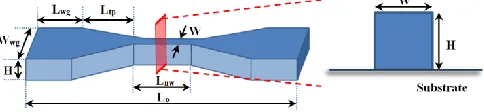
nanowires are designed to be easily connected to other optical devices, such as an optical coupler and an interferometer, by having a feed waveguide and tapered waveguide attached to their ends. The tapered waveguide plays an important role in reducing the power loss when the light couples from the feed waveguide to the small dimensional nanowires [24]. Thus, the power of light interacting with the sensing material is enhanced. The design of the nanowire structure considered in this work and its cross section are shown in Fig. 1.
The integrated nanowire structure consists of the nanowire with length Lnw, the tapered waveguide with length Ltp=270 m
and the feed waveguide with length Lwg as shown in Fig. 1. The
overall structure has a length of Lo=5000 m. The nanowire
width (W) is varied from 0.5 m to 1.0 m but it has a constant height (H) of 0.5 m. For the purpose of this study, the nanowires are designed to have different lengths (Lnw) in each set. A set of
nanowires contains one reference feed waveguide, one reference
tapered waveguide and four different nanowires with lengths 250 m, 500 m, 1000 m and 2000 m. The nanowires of different lengths are used to study the attenuation coefficient αnw.
The purpose of the two reference waveguides is to eliminate the effect of the feed waveguide and the tapered waveguide in the calculation of the attenuation coefficient of the nanowires (αnw).
2.2 Numerical Calculations
To study the behavior of this ormocomp nanowire, the full vectorial H-field finite element formulation [25] has been applied for the modal analyses of the nanowire structure, to determine the propagation characteristics of the fundamental optical mode. There are two approaches which can be used with the FEM, the Raleigh-Ritz variational method and the Galerkin method of weighted residuals. In our case, the variational approach is used and the governing differential equation is not solved directly, but the variational expression is formulated as a functional, as shown in Eq. 1. The functional used to solve the problems is related to the standard eigenvalue problems, and the modal characterization is obtained by minimizing this functional.
𝜔2=∫[(𝛻×H)∗∙𝜀−1(𝛻×H)+𝑝(𝛻×H)∗(𝛻×H)]𝑑𝑥𝑑𝑦
∫H∗∙𝜇H 𝑑𝑥𝑑𝑦 (1)
where H is the full vectorial magnetic field, * represents a complex conjugate and transpose, 𝜔 is the angular frequency of the wave, 𝜔2 is the eigenvalue, and 𝜀 and 𝜇 are the permittivity
and permeability, respectively.
[image:3.612.317.559.245.301.2]In this paper, the possible mode fields and power confinement of ormocomp nanowires are studied over the wavelength, the width and the height of the nanowire structure, and the different cladding materials. First, the structure is designed to be a single Fig. 1: A schematic of the nanowire structure connected with a feed waveguide and a tapered waveguide, and its cross section. The feed waveguide has width Wwg, and length Lwg. The
nanowire (Lnw) with width W and height H is attached to the
tapered waveguide Ltp. The total length of the nanowire structure
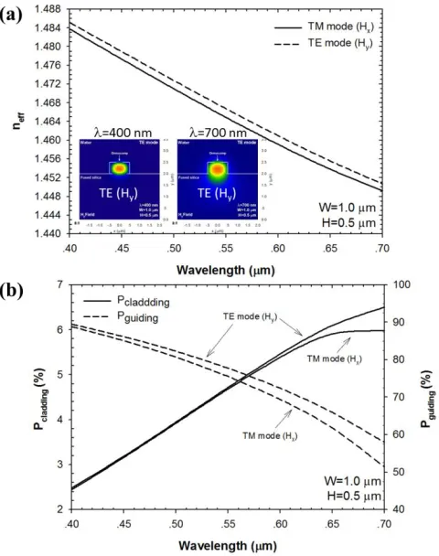
mode nanowire. Therefore, the nanowire is assumed to have a fixed dimension with the width and height of 0.5 m and 1.0 m, respectively. The ormocomp nanowire with refractive index of 1.520 is designed to be on fused silica substrate with the refractive index of 1.446. It is surrounded by water (n=1.333 at room temperature) as the cladding material. The H-field vector formulation of FEM is used to calculate the modal properties of this waveguide structure by varying the wavelength of excitation. In this case, cold white light with operating wavelength between 400 nm and 700 nm is used as a light source. With this structure, both quasi-TM mode (Hx11) and quasi-TE mode (Hy11) are
considered. The variation of the effective index of these allowed modes and the power confinement in each region of the nanowire with respect to the operating wavelength are shown in Figs. 2(a) and 2(b), respectively.
The effective index of the fundamental mode, as shown in Fig. 2(a), decreases with the increasing wavelength for both the quasi
-Fig. 2: (a) The change of effective index over the operating wavelength in the visible region for both quasi-TM and quasi-TE modes. The insets are the modal field profiles excited in the ormocomp nanowire with 1.0 m width, and 0.5 m height at the wavelength 400 nm (left inset) and 700 nm (right inset) for quasi-TE mode. (b) The variation of power confinement in the cladding region (sensing region), and the guiding region (ormocomp) with the operating wavelength for the quasi-TM (H𝑥11) and quasi-TE modes (Hy11).
TM and quasi-TE modes as the waveguide dimension reduces compared to the wavelength. The quasi-TE mode has higher effective index compared to the quasi-TM mode as the width of the waveguide is bigger than its height, which means that the light is more confined in the core region for the quasi-TE mode than the quasi-TM mode, as presented in Fig. 2(b). The insets in Fig. 2(a) show the comparison of the dominant Hy field of the
fundamental quasi-TE mode (Hy11) in the 1.0 m wide and 0.5 m
high ormocomp nanowire with the operating wavelength of 400 nm (left inset) and 700 nm (right inset). As shown in Fig. 2(b), the light is better confined in the guiding region at a lower operating wavelength. Therefore, the evanescent field extending into the cladding region is less compared to the light guided inside the core. The cladding region, where the evanescent field extends, is considered to be the sensing area. Thus, the high power confinement in the cladding is the key parameter to achieve better sensitivity. However, the power loss in the substrate is also greater with the higher operating wavelength because it is close to the cutoff wavelength. To obtain high power confinement in the cladding region together with a good confinement in the guiding area, the 650 nm wavelength (red region) is used as the operating wavelength in the following studies and in the experimental work.
With the fixed operating wavelength at 650 nm (red light source), the effect of the waveguide width on the mode field and power confinement of the fundamental modes has been studied as shown in Fig. 3. The study assumes a structure with the height 0.5 m and width which varies between 0.5 m and 1.0 m. In this case, the cladding media is water (nc =1.333).
Fig. 3: (a) The change of effective index as a function of the structure width in the range between 0.5 m and 1.0 m for both quasi-TM and quasi-TE modes. The insets show the modal field profiles excited at 0.7 m width (left inset) and 1.0 m (right inset) width for quasi-TM mode. (b) The variation of power confinement in the cladding region (sensing region) and guiding region (ormocomp) with respect to the structure width for quasi
-TM (H𝑥11) and quasi-TE modes (H y 11).
[image:4.612.57.297.244.548.2] [image:4.612.319.563.286.594.2]obtained in both the quasi-TM and quasi-TE modes are about 1.446, which is the refractive index of the fused silica substrate. Therefore, the light starts extending into the substrate leading to a large power loss when the width of the structure is less than 0.75 µm. The left inset shows the extension of Hx-field into the
substrate when the structure has 0.70 µm width. The right inset presents the Hx-field confined in the 1.0 µm width structure. For
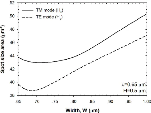
[image:5.612.318.562.318.485.2]Fig. 3(b), the maximum power confinement in the cladding region is achieved when the structure has the width of 0.80 µm. With the width larger than 0.80 µm, the power confinement in the cladding region is slightly decreased due to the better confinement in the core region. For the structure below 0.80 µm, the power confinement in both the cladding and guiding regions are significantly decreased because the power is lost into the substrate. The optical field extends in the substrate due to the cut off limit. The cut off limit for this nanowire structure can also be identified by studying the spot size, which is taken as the area where the field intensity drops to 1/e of its maximum intensity. The change in the spot size with respect to the width of the nanowire is shown in Fig. 4. It can be noted that this waveguide remains single-moded when the width, W, is reduced below 1.55 µm and 1.65 µm, for the quasi-TE and the quasi-TM modes, respectively.
Fig. 4: The variation of spot size area with respect to the width of nanowire which is varied from 0.65 µm to 1.00 µm.
The spot size of the large nanowire increases with its width. This is due to the large volume confinement in the guiding region. The smallest spot size represents the region close to the cut off limit. The quasi-TM mode has bigger spot size compared to the quasi
-TE mode and approaches its cut off limit before the quasi-TE mode. For the quasi-TM mode, the structure is close to the cut off when reducing the structure width to 0.80 µm whereas the nanowire structure can be scaled down to 0.70 µm for the quasi
-TE mode. For the small nanowire below the cut off limit, the spot size becomes larger due to the expansion of the light in the substrate.
To prevent the nanowire to be in the cut off region, the nanowire with 1.0 m width and 0.5 m height operated at 650 nm wavelength is considered in the next study. The nanowire is intended to be used in biosensing applications, so the study of the sensitivity over the cladding material, which is mostly in solution form, is studied. The refractive index of the cladding medium is
varied in the range of 1.333 to 1.400. The sensitivity of the nanowire (S) can be calculated by obtaining the effective index difference (∆𝑛𝑒) over the change of refractive index of the cladding material (∆𝑛) as follows [26]:
𝑆𝑒𝑛𝑠𝑖𝑡𝑖𝑣𝑖𝑡𝑦 (𝑆) =∆𝑛𝑒
∆𝑛 (2)
where ∆𝑛𝑒 and ∆𝑛 can be obtained as follows:
∆𝑛𝑒=
𝑛𝑒−𝑛𝑒,𝑟𝑒𝑓
𝑛𝑒,𝑟𝑒𝑓 (3)
∆𝑛 =𝑛𝑐−𝑛𝑐,𝑟𝑒𝑓
𝑛𝑐,𝑟𝑒𝑓 (4)
where𝑛𝑐 is the refractive index of cladding material varied from
1.333 to 1.400 in this case, 𝑛𝑐,𝑟𝑒𝑓 is the reference refractive index
which is 1.333 (water), 𝑛𝑒 is the effective index obtained with the
presence of each cladding material and 𝑛𝑒,𝑟𝑒𝑓 is effective index
[image:5.612.53.295.335.516.2]obtained with the water cladding. The sensitivity of this nanowire structure with respect to the change of cladding material is shown in Fig. 5.
Fig. 5: The sensitivity and the cladding percentage power confinement of the nanowire when the refractive index of cladding material is varied from 1.333 (water) to 1.40.
It can be observed from Fig. 5 that the sensitivity of the nanowires (presented along left y-axis) exploiting quasi-TM mode is greater than that of the quasi-TE mode, and this value increases when the refractive index of the cladding material is increased. Even though the quasi-TE mode has greater effective index, the effective index changes with respect to the cladding index is less. The greater effective index difference in the quasi
-TM mode can be enhanced by increasing the field intensity at the interface between the cladding material and the guiding region where the evanescent field exists. It can be observed from the change in the cladding power confinement with the variation of the refractive index, shown along the right y-axis of Fig.5, that as the cladding refractive index increases, the Power confinement in the cladding also increases, thus improving the sensitivity of the device.
3. Fabrication Process
The polymer nanowire is fabricated using the nano-imprint method. It is basically the method to transfer the pattern from the silicon master nanowire onto the ormocomp layer. Below, the fabrication process of the silicon master and ormocomp nanowires are discussed. As mention earlier, the dimensions of the nanowires to be fabricated are fixed at the width of 1.0 m and height of 0.5 m. The nanowires are fabricated as a set with different lengths. The four different nanowires lengths considered here are 250 m, 500 m, 1000 m, and 2000 m. In addition, the feed waveguide and tapered waveguide references are included in the set.
3.1 Silicon nanowire fabrication
The ormocomp nanowire can be obtained by transferring the pattern from the silicon nanowire. Therefore, the master silicon nanowire needs to be hard mold in the nano-imprint technique. The main fabrication process of silicon nanowires includes photolithography and wet etching. The silicon nanowires are fabricated on a 6-inch silicon wafer. First, the oxide layer is deposited on the substrate using low pressure chemical vapor deposition (LPCVD) at 1000C. Then 1.09 m thickness of sumitomo PFI-34A photoresist is spin-coated on the oxide layer. The pattern of the set of nanowires is transferred onto the photoresist layer by UV exposure for 340 ms. The power of the UV lamp in this treatment delivers 350.81 mW/cm2. After post
-baking at 110C for 3 mins, the photoresist is developed using tokuyama SD-W for 60 s. The hard bake then needs to harden the photoresist pattern and prepare it for the next oxide etch. Buffered oxide etch (BOE) is used to etch the oxide layer. It is a wet etch made of 40% ammonium fluoride (NH4F) and 49%
hydrofluoric acid (HF) in the volume ratio of 6:1. Finally, piranha solution is used to remove the residual photoresist on the silicon nanowire pattern. Piranha is a solution made of 70% sulfuric acid (H2SO4) and 30% hydrogen peroxide (H2O2) with the ratio of 4:1.
A SEM image of the fabricated nanowire is shown in Fig. 6.
Fig. 6: (a) SEM image of the nanowires in one set including two reference waveguides and four different lengths of nanowires. (b) The magnified SEM image at the part of the nanowire involving the sidewall surface and cross section.
The fabricated set of silicon nanowires consisting of four different lengths of nanowires and two reference waveguide can be seen in Fig. 6(a). Fig. 6(b) shows the magnified part of the silicon nanowire including the sidewall surface and cross section. The surface roughness is clearly seen in the Fig. 6(b) and it is measured to be around 0.1 µm. Even though, the silicon nanowire is designed to have a vertical sidewall, the wet etching makes the nanowire to have non-vertical sidewalls. Measurements show that the sidewall angle is around 75.
3.2 Ormocomp nanowire fabrication
The polymeric material ormocomp is used to fabricate the polymer nanowire. It is a UV curable material for the nano
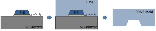
[image:6.612.314.564.381.431.2] [image:6.612.52.296.464.556.2]-imprint process with a refractive index of 1.52. To perform the nano-imprint process, the nanowire pattern is transferred from the master silicon nanowire onto the ormocomp layer using PDMS (Polydimethylsiloxane). The silicon nanowire is considered to be the hard mold whereas the PDMS is considered to be the soft mold in the nano-imprint technique. First, the PDMS has to be prepared by mixing the silicone elastomer base and curing agent with the ratio of 7:1 by weight. This ratio can be varied depending on the desired hardness of the PDMS mold. The mixture is then coated on the desired master silicon nanowire and undergoes the degas process for 30 minutes in order to remove all the bubbles. To harden the PDMS, it is cured at the temperature of 100 C. After the curing process, the PDMS is removed from the silicon substrate. The pattern created on the PDMS soft mold is the reverse pattern of the silicon nanowire. The process flow to obtain the PDMS soft mold is shown in Fig. 7. The next step is to transfer the pattern from the PDMS soft mold onto the ormocomp layer. The ormocomp nanowire is fabricated on a glass substrate. First, the ormocomp is dispensed on the substrate. Next the PDMS mold is used to stamp the nanowire pattern on the ormocomp layer. Then, the ormocomp is cured with UV light for 5 minutes. After that the PDMS is removed. The same pattern with the silicon hard mold is now expected to appear on the ormocomp layer. The nano-imprint process using PDMS stamped on ormocomp layer is shown in Fig. 8.
Fig. 7: The preparation of the PDMS soft mold from the master silicon nanowire which is used as the hard mold for the nano-imprint technique. The reversed pattern of silicon nanowire is obtained in the PDMS soft mold.
Fig. 8: A schematic showing the process flow of the nano-imprint technique used to obtain the ormocomp nanowire.
[image:6.612.315.562.486.570.2]Fig. 9: An optical image of (a) a set of nanowires, (b) magnified image of the nanowire set consisting of the feed waveguide, the tapered waveguide, and four different lengths of nanowires, (c) feed waveguide and tapered waveguide and (d) 1 m width nanowire. The inset is the AFM image of 1
m width ormocomp nanowire and its cross section.
The optical microscope images of the ormocomp nanowire at different magnifications are seen in Fig. 9. The non-vertical sidewall structure can also be observed from the optical microscopic image as shown in Fig. 8(d). The upper width is measured to be 1.03 m, and the lower width is measured to be around 1.55 m. This result agrees the image obtained from the AFM as shown in the inset. From the AFM, the width at the top surface is 1.0 m whereas the width at the substrate is 1.6 m.
4. Results and Discussions
In this section we present the results from the actual fabricated nanowires. The nanowire from the fabrication process has a rib structure with the slab thickness (t) due to the residual ormocomp layer. The nanowire core has a non-vertical sidewall structure (slanted-shaped waveguide). The sidewall angle is measured to be in the range of 60 to 75. Numerical simulations of the possible mode field, the power confinement, and the sensitivity are carried out for different slab thicknesses, operating wavelengths and cladding materials. This slant-shaped waveguide has the fixed dimension of 0.5 µm height, 1.0 µm top
-width, and 1.5 µm bottom-width. A red light source with operating wavelength of 633 nm is used in the experiment. The cladding material considered in the simulation has a refractive index in the range between 1.333 and 1.400. For the experiment glycerol solution with refractive indices of 1.333 and 1.363, respectively, at room temperature are used as the cladding mediums.
4.1 Simulation Results for Non-Vertical Sidewall Nanowires The fundamental mode field inside the nanowire is studied using the full-vectorial finite element method. The slab thickness obtained from the fabrication is measured to be around 2 µm. By changing the slab thickness (t), the characteristic of the polymer rib nanowire with non-vertical sidewall can be modified. The change of effective index when varying the slab thickness for quasi-TM and quasi-TE modes is shown in Fig. 10.
Fig. 10: The graph of effective index change with respect to the slab thickness (t) for the rib-nanowire with the height of 0.5 µm and the top
-width of 1.0 µm. The insets show the fundamental H-field for quasi-TM mode (left) and quasi-TE mode (right) guided in the rib-nanowire with slab thickness of 2.0 µm.
Similarly to the designed structure nanowire, the quasi-TE mode has a slightly higher effective index than the quasi-TM mode. With the slab thickness between 1 to 5 µm, the effective index is increased dramatically when the slab layer is larger. For the slab thickness greater than 5 µm, the core height of the nanowire is too small compared to the slab layer which cannot influence the change in the effective index of the whole structure. Therefore, the effective index value becomes almost constant at around 1.52 which is the refractive index of the nanowire. The insets show the H-field for quasi-TM mode (left) and quasi-TE mode (right) for the structure with the slab thickness of 2.0 µm.
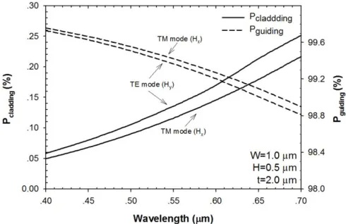
Next, a fixed slab thickness of 2 µm is considered to study the characteristic of the nanowire over the operating wavelength and cladding material as it exhibitsa better confinement. The change in power confinements in the core and cladding regions over the wavelength are presented in Fig. 11.
Fig. 11: The graph of power confinements in the cladding and guiding regions in quasi-TM mode nanowire with non-vertical sidewall with the operating wavelength in the visible region (400-700 nm).
[image:7.612.53.297.61.239.2] [image:7.612.316.561.482.641.2]increased. Therefore, there is less confinement of the optical field in the guiding region at a large wavelength.
The sensitivity of this ormocomp rib nanowire with non
-vertical sidewall calculated from Eq. 2 is shown in Fig. 11.
Fig. 12: The sensitivity of rib-ormocomp nanowire with non-vertical sidewall when the refractive index of cladding material is varied in the range of 1.343 to 1.400.
The sensitivity of the nanowire is improved when increasing the refractive index of the cladding material for both the quasi-TM and quasi-TE modes. Similarly as for the nanowire shown in Fig. 5, for the ridge nanowire, the quasi-TM mode also has higher sensitivity than the quasi-TE mode as shown here. However, the fabricated nanowires have two orders of magnitude lower sensitivity than the designed nanowire since the fabricated rib waveguide modal field shifts away from cladding region to the lower planar slab region
Highly slanted waveguides can induce polarization rotation, thus leading to mode coupling [27]. The above effect has been considered in the simulations of the device, however, found not to have a significant contribution due to the lower index contrast and nearly symmetrical deformation of the structure examined in the present work.
4.2 Experimental Results for Non-Vertical Sidewall Nanowires This section contains two main parts, the optical imaging and attenuation coefficient extraction (). The slant-shaped ormocomp nanowires obtained from the nano-imprint method are used in the experiment. The optical experiment is performed to image the optical field at the output of the signal guided along the nanowire. The optical image is then processed to obtain the intensity which is later used to extract the attenuation coefficient of the nanowire (nw). The operating wavelength in the
experiment is 633 nm which is the red light source. The three cladding mediums used are air (n=1.000), water (n=1.333)and glycerol solution (n=1.363).
4.2.1 Optical Imaging
The optical setup to image the signal consists mainly of a red LED light source (=633 nm) connected with a single mode optical fiber, the sample stand and two CCD cameras. The light source and the CCD cameras are places on a xyz stage. The schematic of the optical setup to image the optical output signal is demonstrated in Fig. 13.
Fig. 13: (a) A schematic showing the optical setup to image the optical field output signal. (b) The actual optical set up.
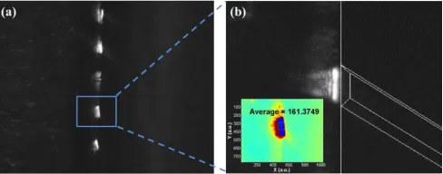
The red LED is connected to a single mode optical fiber and it is used as a light source (650 nm) as shown in Fig. 13. An objective lens with a magnification of 20x is used to focus the light, and also to enhance the input signal. For the alignment process, the objective lens with the magnification of 10x connected with CCD camera is placed on the top of nanowire stand. It is used to align the optical fiber and the ormocomp nanowire. Following the alignment, the focused light is coupled into the specific nanowire, and then propagates along the wire. The output signal is detected by another CCD camera connected by a 20x objective lens which is used to magnify the output image. The optical output detected by the CCD camera is shown in Fig. 14. The image of the optical field output is then processed to extract the output intensity. In order to extract the average output intensity from the CCD camera image, the highest intensity point in the image needs to be located first. After that, the points where the intensity is more than 70% of the maximum intensity have to be located. The high intensity points are now scattered. Therefore, the center of scattering is marked, and enclosed by the square boundary. The average intensity is finally calculated from the intensity profile located inside the boundary. The average intensity of one nanowire is presented in the inset of Fig. 14(b).
It can be observed that the optical field image obtained from the CCD camera, as shown in Fig. 14(b), matches with the optical field image from the simulation shown in Fig. 9(b), where the field is more confined in the substrate region.
Fig. 14: The average intensity image of the output signal for (a) feed waveguide and (b) nanowire with the length of 2000 µm. The insets are the optical field image at the output detected by the CCD camera.
[image:8.612.314.562.55.211.2] [image:8.612.51.299.103.281.2] [image:8.612.319.563.533.629.2]4.2.2 Attenuation Coefficient Extraction
After extracting the output intensity from the nanowire, the attenuation coefficient can be calculated using Beer-Lambert law:
𝐼 = 𝐼𝑜𝑒−2𝛼𝐿 (5)
where 𝐼 is the intensity of the transmitted light, 𝐼𝑜is the intensity
of the incident light, 𝛼 is the attenuation coefficient, and 𝐿 is the path length. However, since the proposed nanowire structure is also enhanced by the feed and tapered waveguides,their attenuation coefficients (wg and tp) are also presented together
with the attenuation coefficient of the nanowire (nw). By
rearranging Eq. 5, the relation of each attenuation coefficient can be derived as a linear equation as shown below:
ln (𝐼𝑗
𝐼𝑜) = 2(𝛼𝑤𝑔− 𝛼𝑛𝑤)𝐿𝑛𝑤 𝑗 − [2𝛼
𝑤𝑔(𝐿𝑜− 2𝐿𝑡) + 4𝛼𝑡𝑝𝐿𝑡𝑝]
(6)
The intensity of incident light in this work (𝐼𝑜) is the intensity of the light transmitted from the reference feed waveguide (wire no.6 in Fig. 8(b). The intensity of the transmitted light (𝐼𝑗) represents the intensity of the light transmitted from each nanowire. The term [2𝛼𝑤𝑔(𝐿𝑜− 2𝐿𝑡) + 4𝛼𝑡𝑝𝐿𝑡𝑝] is the constant
term and the term2(𝛼𝑤𝑔− 𝛼𝑛𝑤) = is the slope of the linear
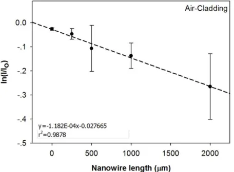
equation. The ratio of light transmitted inside the non-vertical sidewall nanowire over the feed waveguide with air-cladding can be fitted into a linear plot as demonstrated in Fig. 15.
With the air-cladding, the relation of the attenuation coefficient between the feed waveguide and the nanowire, obtained from slope, can be presented by 2(𝛼𝑤𝑔− 𝛼𝑛𝑤)
==-1.1824 cm-1 where the negative sign represents a greater
attenuation coefficient in the nanowire than the feed waveguide. This is due to the smaller size of the nanowire which suffers from higher losses. In the experiment, water (n=1.333) and glycerol solution (the mixture of water and glycerol with the volume ratio of 4:1, n=1.363) are also considered as cladding mediums. For the water-cladding, the calculated is about -0.7546 cm-1 whereas
of -0.6980 cm-1 is obtained for glycerol solution-cladding.
[image:9.612.317.562.510.674.2]The difference between the attenuation coefficients () is reduced when the refractive index of cladding material is increased. The change in over the different cladding materials achieved from the experiment is shown in the Fig. 16.
Fig. 15: The linear relation between ln(𝐼𝑗/𝐼𝑜) and length of the nanowire
(𝐿𝑗𝑛𝑤) where the slope is 2(𝛼𝑤𝑔− 𝛼𝑛𝑤).
The power confinement in the guiding region is smaller with an increase of the refractive index of the cladding material (smaller n). Hence, the attenuation coefficient is increased if the nanowire with a smooth surface is considered. However, the fabricated nanowire does not have asmooth surface. The surface roughness arises from the fabrication process used here, and this causes the scattering loss. The increase of the cladding-index minimizes the difference of the refractive index between core and cladding (n). Hence, the scattering from the surface is reduced leading to a smaller attenuation coefficient. In this work, only the scattering from the interface between core and cladding is considered. The scattering effect from the core-substrate interface is assumed to be very small and can be negligible. The relation between scattering from surface roughness and the attenuation coefficient () derived from simple theory of surface scattering [23, 28] is defined as follows:
α = 4𝜎2𝜅3
𝛽(ℎ+2 𝛾⁄ ) (7)
where is the root-mean-squares surface roughness, 𝜅 is the transverse propagation constant in the core region (𝜅 = √𝑘𝑜2𝑛2− 𝛽2), is the transverse propagation in cladding region
(𝛾 = √𝛽2− 𝑘𝑜2𝑛2), is the modal propagation constant, and h is
the thickness of the nanowire. The average surface roughness of ormocomp nanowires measured from AFM is found to be around 0.10 µm. The change of attenuation coefficient () due to scattering effect with different cladding material is calculated and shown in Fig. 16.
It can be observed from Fig. 16 that the variation of attenuation coefficient with respect to the refractive index of cladding material has the same trend for both numerical simulation work and experimental measurements. The attenuation coefficient is decreased as the refractive index of the cladding material is increased. This is due to the scattering effect from the surface roughness. However, higher loss shown in the simulations could be due to the value of surface roughness () consider here. Besides that experimental results shows the differential loss (subtracting the substrate loss, wg) but the
numerical simulations calculated the overall possible scattering loss values.
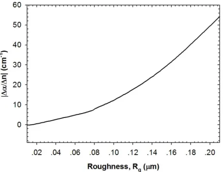
[image:9.612.51.279.535.703.2]To study the sensitivity of the nanowire affected by the scattering from surface roughness, the change of attenuation coefficient over the change of refractive index of cladding material is calculated. In this paper, the attenuation coefficient difference when changing the cladding material from water (n=1.333) to glycerol solution (n=1.363) is investigated over the root-mean
[image:10.612.52.282.135.313.2]-square roughness (Rq) as shown in Fig. 17.
Fig. 17: The change of attenuation coefficient over the change of cladding material with respect to surface roughness in the numerical calculations.
With the same cladding material, the nanowire structure with rough surface has a higher scattering loss than a nanowire with a smooth surface. The scattering loss at the surface of the nanowire enhances the sensitivity because there is more light interaction at the interface between the core and cladding regions. Fig. 17 shows the normalized value of the change in the attenuation coefficient over the change in the cladding-index with respect to the surface roughness for the calculation work. In the experimental work, the change of attenuation coefficient over the change of cladding refractive index is around 1.88 cm-1 with the
surface roughness of 0.10 µm. It has lower sensitivity compared to the calculation which may be due to the external factor such as human error and instrument resolution.
5. Conclusion
This paper presents apolymer nanowire as an optical transducer fabricated using the nano-imprint technique which is simpler, and cheaper than other techniques. The polymeric material used in the fabrication isormocomp with refractive index of 1.52. The ormocomp nanowire is designed to be able to detect maximum change of effective index when the cladding
-index is changed. The possible mode fields and the power confinement in the cladding region (sensitive area) in quasi-TM and quasi-TE modes are studied in order to optimize the dimension of the nanowire structure. The smaller nanowire has higher sensitivity due to the extension of the optical field in the cladding area. However, due to instrument limitations in the fabrication process, the non-vertical sidewall nanowire with 1.0 µm wide and 0.5 µm high was the smallest possible nanowire obtained for this work. The sensitivity of the non-vertical sidewall nanowire is less than the vertical sidewall structure. With higher refractive index of cladding material, the optical field is extended deeper into the cladding area, thus causing the higher attenuation coefficient when the surface roughness is neglected
for an ideally smooth surface. Nevertheless, the attenuation coefficient tends to reduce when increasing the cladding-index. This is because the light scattered from surface roughness of core/cladding region is reduced when changing the cladding medium from water (n=1.333) to glycerol solution with a higher index (n=1.363). Therefore, the scattering loss is the dominant factor in this work. The scattering effect from the rougher surface provides a greater change in attenuation coefficient over the change of refractive index.
Further enhancement of this surface can be achieved by coating the top surface of the fabricated nanowire with a metallic layer, thus improving the sensitivity of the fabricated nanowire. The metal layer, such as gold for example, exhibits surface plasmon resonance and improves the sensitivity of the nanowires.
References
1.G. Shen, P.-C. Chen, K. Ryu, and C. Zhou, "Devices and chemical sensing applications of metal oxide nanowires," Journal of Materials Chemistry 19, 828-839 (2009). 2.M. Yun, N. V. Myung, R. P. Vasquez, J. Wang, and H.
Monbouquette, "Nanowire growth for sensor arrays," in Optical Science and Technology, SPIE's 48th Annual Meeting, (International Society for Optics and Photonics, 2003), 37-45.
3.C. Themistos, M. Rajarajan, B. M. A. Rahman, and K. T. V. Grattan, "Characterization of silica nanowires for optical sensing," J. Lightwave Technol. 27, 5537-5542 (2009). 4.B. Adhikari and S. Majumdar, "Polymers in sensor
applications," Progress in polymer science 29, 699-766 (2004).
5.D. M. Leung, X. Kan, B. M. A. Rahman, N. Kejalakshmy, and K. T. V. Grattan, "Optimizing the power confinement in silicon slot waveguides by use of Finite Element Method," in SPIE/OSA/IEEE Asia Communications and Photonics, (International Society for Optics and Photonics, 2011), 83071A-83071A-83076.
6.F. Dell’Olio and V. M. Passaro, "Optical sensing by optimized silicon slot waveguides," Opt. Express 15, 4977-4993 (2007).
7.D. J. Sirbuly, A. Tao, M. Law, R. Fan, and P. Yang, "Multifunctional nanowire evanescent wave optical sensors," Advanced Materials 19, 61-66 (2006).
8.B. MacCraith, V. Ruddy, C. Potter, B. O'Kelly, and J. McGilp, "Optical waveguide sensor using evanescent wave excitation of fluorescent dye in sol-gel glass," Electronics letters 27, 1247-1248 (1991).
9.J. Lou, L. Tong, and Z. Ye, "Modeling of silica nanowires for optical sensing," Opt. Express 13, 2135-2140 (2005). 10.J. Wang and D. Dai, "Highly sensitive Si nanowire-based
optical sensor using a Mach–Zehnder interferometer coupled microring," Optics letters 35, 4229-4231 (2010). 11.C. Viphavakit, N. Atthi, S. Boonruang, C. Themistos, W.
S. Mohammed, K. Kalli, B. A. Rahman, and M. Komodromos, "Characterization of polymer nanowires fabricated using the nanoimprint method," in SPIE Photonics Europe, (International Society for Optics and Photonics, 2014), 912632-912632-912610.
12.J. Huang, S. Virji, B. H. Weiller, and R. B. Kaner, "Polyaniline nanofibers: facile synthesis and chemical sensors," Journal of the American Chemical Society 125, 314-315 (2003).
highly sensitive optical sensors," Nano Lett 2, 1273-1275 (2002).
14.K. Ramanathan, M. A. Bangar, M. Yun, W. Chen, N. V. Myung, and A. Mulchandani, "Bioaffinity sensing using biologically functionalized conducting-polymer nanowire," Journal of the American Chemical Society 127, 496-497 (2005).
15.H. Liu, J. Kameoka, D. A. Czaplewski, and H. G. Craighead, "Polymeric Nanowire Chemical Sensor," Nano Lett 4, 671-675 (2004).
16.F. Gu, L. Zhang, X. Yin, and L. Tong, "Polymer single-nanowire optical sensors," Nano Lett 8, 2757-2761 (2008). 17.H. Liu, J. Kameoka, S. Verbridge, and H. G. Craighead,
"Polymeric Nanowire Architecture and Nanodevices," (Cornell University, Aug., 2005).
18.J. Kameoka, D. Czaplewski, H. Liu, and H. Craighead, "Polymeric nanowire architecture," J. Mater. Chem. 14, 1503-1505 (2004).
19.S. A. Harfenist, S. D. Cambron, E. W. Nelson, S. M. Berry, A. W. Isham, M. M. Crain, K. M. Walsh, R. S. Keynton, and R. W. Cohn, "Direct drawing of suspended filamentary micro-and nanostructures from liquid polymers," Nano Lett 4, 1931-1937 (2004).
20.N. T. Kemp, D. McGrouther, J. W. Cochrane, and R. Newbury, "Bridging the gap: polymer nanowire devices," Advanced Materials 19, 2634-2638 (2007).
21.H. Fang, D. Yuan, R. Guo, S. Zhang, R. P. Han, S. Das, and Z. L. Wang, "Fabrication of Patterned Polymer Nanowire Arrays," ACS nano 5, 1476-1482 (2010).
22.L. J. Guo, "Nanoimprint lithography: methods and material requirements," Advanced Materials 19, 495-513 (2007).
23.P. Tien, "Light waves in thin films and integrated optics," Appl Opt 10, 2395-2413 (1971).
24.C. Viphavakit, C. Themistos, M. Komodromos, N. Atthi, S. Boonrueng, W. S. Mohammed, and J. Dutta, "Development of integrated microfluidic device for optical flow rate sensing," Journal of Circuits, Systems, and Computers 22(2013).
25.B. M. A. Rahman and J. B. Davies, "Finite-element solution of integrated optical waveguides," Lightwave Technology, Journal of 2, 682-688 (1984).
26.S. Boonruang and W. S. Mohammed, "Effect of the cladding layer on resonance response in guided mode resonance structures and its sensing applications," JOSA B 28, 671-678 (2011).
27.B. M. A. Rahman, S. S. A. Obayya, N. Somasiri, M. Rajarajan, K. T. V. Grattan, and H. A. El-Mikathi, Design and Characterization of Compact Single-Section Passive Polarization Rotator", Journal of Lightwave Technol., 19, 512-518 (2001).