International Journal of Innovative Technology and Exploring Engineering (IJITEE) ISSN: 2278-3075, Volume-8 Issue-10, August 2019
Abstract: This paper presents the removal of initial phase transient currents in an existing dc-dc boost converter topology with the help of a modified switched inductor cell. In an earlier proposed topology, a novel single switch boost converter was proposed with high voltage gain, which however gave a high initial transient current of the order of 26kA on simulating in MATLAB Simulink environment. This initial phase current was removed by placing a small valued inductor and a freewheeling diode in series with boost capacitor. The inductor is placed in parallel with the diode and creates an open circuit initially, this arrangement limits the current to a bearable value, i.e. approximately 180A, without compromising with the high gain of the cell. The results of the proposed modifications are validated using MATLAB Simulink.
Keywords: dc-dc converter, switched inductor cell (SIC), switched inductor switched capacitor (SISC), switched capacitor cell (SCC).
I. INTRODUCTION
Nowadays, distributed power generation has gained excessive attention, especially in the field of non-conventional energy sources owing to fast depletion of fossil fuels and greenhouse gas emission [1]. The solar energy, over the years has become a necessary non-conventional clean energy resource [2]. Output power from the solar panel is low, however several panels needs to be linked in a series-parallel fashion to improve the output [3]. Voltage accessible from the series-parallel arrangement of solar PV cells is in of the order of 20–60 V. Interfacing of the PV panels with the load requires an optimal energy converter. In many applications such as renewable energy-based power generation scheme, a dc-dc boost converter achieves importance in order to increase the voltage at the output [4]. To achieve a high voltage gain, in applications such as solar-based power generation, an isolated dc-dc converters is not the preferred alternative owing to issues such as transformer core saturation at high frequency, low effectiveness, bulk in size etc. [5]. For obtaining large voltage gain at a high duty ratio, the standard dc-dc boost converters with non-isolated topologies suffers
Revised Manuscript Received on August 05, 2019
Preeti Gupta, Electrical Engineering Department National Institute of Technical Teachers Training and Research Chandigarh, India.
Shimi S.L., Electrical Engineering Department National Institute of Technical Teachers Training and Research Chandigarh, India.
from the issues such as reverse-recovery problems of diode and high voltage stress on switching devices. The shortcomings of isolated converter topologies can be readily eliminated with the help of non-isolated converters [6]. Combinations of different voltage lifting methods are discussed in [7], for various non-isolated high-gain dc-dc converter topologies for PV systems. Cascaded technique is one of the simplest methods to increase the voltage gain however, its second stage suffers from the problem of instability, reverse recovery of the diode and high voltage stress on the switch. High voltage gain is achieved from the voltage multiplier technology [8] unfortunately, when the voltage gain exceeds 10 the power handling capability decreases [9]. Topologies in which coupled inductors are used provide high voltage gain. But leakage inductance creates severe issues such as Electromagnetic Interference (EMI) and resonance in power circuit. To lift the voltage, various voltage lifting methods incorporated with coupled inductor-based topologies are used such as switched capacitor cells, voltage multiplier cell etc. [10]. Boost converters with switched capacitor-based can deliver a high voltage gain, and minimum voltage stress on power switch by charging the capacitors parallel and discharging them in series. But the voltage regulation of these types of converters is weak [11, 12]. Zeta based converters consists of switched capacitor cells, can deliver large voltage gains [13]. However, when the input current is discontinuous, it becomes unsuitable for renewable photovoltaic applications. Boost converters consists of switched inductor cells, are convenient to increase the voltage gain with large passive elements by energizing the inductors in parallel and discharging them in series [11]. Converters based on passive switched inductors, the entire switched inductor cell is connected in series with a single active switch [11]. However, for active switched inductor network, an active switch is connected with every inductor for reducing the voltage stress of active switches, requiring higher number of components [14]. A high gain is achieved in combined active and passive SI cells, though it requires a larger number of active switches and has a large overall component count. This leads to high conduction and switching losses [15]. In this paper, the authors proposed a novel methodology to reduce the initial current burst in a switched inductor-switched capacitor (SISC) based non-isolated single switch
dc-dc boost converter.
Removal of Initial Phase Transient Current in
DC-DC Boost Converter using Modified
Switched Inductor
The simulation of both original and modified topologies is carried out in MATLAB-Simulink® environment and results are compared. The topology developed in [16], is used to test the voltage gain in transient and steady state conditions. In the proposed topology, the passive SI cell is modified to remove the initial enormous transient current burst. For the purpose, a small inductor and a freewheeling diode are used as additional components for removing the transients caused by the boost capacitor. The proposed modification does not reduce the gain of the converter cell, however improves the transient switching characteristics as evident in the simulation results. Also, in both topologies the ripples are found to be negligible in the output.
II. DC-DCCONVERTERWITHSWITCH
INDUCTORCELL
In this the performance of the passive switched inductor cell (SIC) has been improved with some modifications.
A. Passive Switched Inductor cell
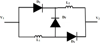
Passive Switched Inductor cell is shown in Fig. 1. Those boost converter which consist of passive switched inductor cell in Place of inductor give much higher gain as in this two energy storing elements are present L1 & L2. When the
switch is ON L1 & L2 energize in parallel as the diode D1 &
D2 become forward biased and DF is reversed biased. When
the switch is OFF the L1 & L2 supply the store energy in series
as in this mode DF is forward biased and D1 & D2 reversed
[image:2.595.316.519.330.423.2]biased.
Fig. 1. Passive Switched Inductor cell B. Modified Switched Inductor cell
[image:2.595.86.260.424.498.2]The modified switched inductor cell is shown in Fig. 2. It gives much higher gain in comparison to passive SIC as it consist of three energy storing elements. The operation of modified switched Inductance cell can be explained as given below.
Fig. 2. Modified Switched Inductor cell Mode 1: When the switch is ON
L1 & L2 and boost capacitor CB energize in parallel as the
diode D1 & D2 become forward biased. Mode 2: When the switch is OFF
in this mode D1 & D2 are reversed biased.
The switched inductor cell [16] gives higher gain as there are three energy storing elements are present. But, the initial value of the charging current is enormous which can damage the system because the initial voltage across CB is zero &
currents through L1 & L2 are also zero. When switch is
turned on, both inductance L1 & L2 are energized through D1
& D2 respectively. CB is also charged through D1 & D2. Since
initial voltage across CB is zero and there is insignificant
resistance of the circuit elements VIN, D1, CB, D2 and switch
S. Therefore, initial value of the charging current is enormous. This high initial current can be minimized by connecting a resistance in series with CB but, this will
increase loses.
C. Proposed modified switched inductor cell
So, author modified the SIC as shown in Fig. 3 in which initial current is limited without compromising with gain. For this the diode of SIC was replaced by a boost capacitors CB with small inductor L01 in series and freewheeling diode
DF is placed in parallel to inductor L01.
Fig. 3.Modified Switched Inductor cell
The operation of modified switched Inductance cell can be explained as given below.
With zero initial values, the charging current of C is as follows:
(1)
(2)
Where is the characteristic impedance of series
LC circuit and is the natural frequency of oscillation and
is given by .
According to the equation (1) the current rises sinusoidally and at the end of half cycle, it becomes zero and VO rises to
2Vin. When switch is turned OFF, the components L1, L2, &
CB are in series and they release their energies to the circuit
on their right side. Now, the capacitor is not required to discharge through L. These discharge current flows throw the freewheeling diode DF. In comparison to single inductor
circuit, there are three energy storing components in SIC, so that the gain increases significantly without enormous initial current initially. It can be validated by MATLAB/Simulink. Switched capacitor cell (SCC)
[image:2.595.85.265.620.697.2]International Journal of Innovative Technology and Exploring Engineering (IJITEE) ISSN: 2278-3075, Volume-8 Issue-10, August 2019
[image:3.595.320.523.52.281.2]switches. This is accomplished by charging the capacitors in parallel and discharging them in series.
Fig. 4.Switched Capacitor Cell
III. SIMULATIONRESULTS
The small inductor is connecting in series of boost capacitor CB and a freewheeling diode in parallel to the inductor. The
[image:3.595.90.253.79.214.2]working of this modified SIC is explained above. Its parameters are given below. This topology is simulated in MATLAB as shown in Fig. 5. The specifications of components used in original and proposed topologies are given in Table I and Table II respectively.
Table- I: Specifications of dc-dc converter
S. No. Specification Value
1 DC voltage source 34 V
2 Inductors 180 µH
3 Capacitor CB 15 µF
4 Capacitor C1, C2, 10 µF
5 Output capacitor 4.7 µF
6 Duty Ratio 0.65
Fig. 5. Simulation Model Of Existing Topology
[image:3.595.331.530.318.706.2]Fig. 6. Simulation Results Obtained For Existing Topology
Table- II: Specifications Of Proposed Dc-Dc Converter
S. No. Specification Value
1 DC voltage source 34 V
2 Inductors 180 µH
3 Inductor LB 10 µH
4 Capacitor CB 15 µF
5 Capacitor C1, C2, 10 µF
6 Output capacitor 4.7 µF
7 Duty Ratio 0.65
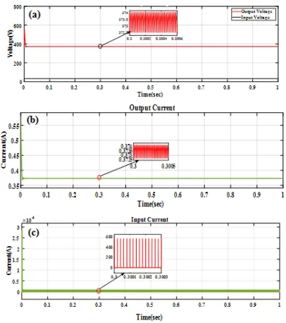
[image:3.595.80.257.360.748.2]Fig. 8. Simulation Results Obtained For Proposed Topology
IV. DISCUSSION
In this paper, a different and novel methodology is proposed to eliminate the starting current spikes. These current spikes, Fig. 4, originate due to the capacitor C1 placed between the
different potential points, i.e. the upper and lower inductor branches of switched inductor cell. In initial phase, the capacitor become short circuited which causes the current to shoot up to approximately 26kA is given in Fig. 7(c). The proposed alteration in given topology removes this problem by in which initial current is limited without compromising with gain. This can be confirmed from input current waveform in Fig. 8(c), with initial transient current to 180A. Also, the circuit offers high voltage gain with addition of only two passive components in the circuit.
V. CONCLUSION
In this paper, a non-isolated step-up modified switched inductor/switched capacitor-based dc-dc converter topology is proposed where the initial burst of current is eliminated by using only two passive components a diode and an inductor, in this a low value of inductor is used in series to the boost capacitor along with a freewheeling diode in parallel to the inductor. This arrangement allows the circuit to establish on startup while maintaining the high gain offered by originally modified switched inductor cell presented in this paper.
This novel modification yielded a voltage gain of 10.96 which is slightly less than the voltage gain of the existing topology, i.e. 11. The simulation results are presented for both originally proposed as well as the modified SIC in this paper. The proposed methodology in this paper does not increase the size of the converter because of low value of inductor. The main advantage of the present study is the use of only single active switch, thus offering better component utilization and further ease of implementing control
algorithms. This converter can be used for interfacing the PV panels with dc micro grid and medium voltage dc bus. Future research can be directed towards further decreasing the starting current and increasing the voltage gain.
REFERENCES
1. M. Z. Jacobson and M. A. Delucchi, "Providing all global energy with wind, water, and solar power, Part I: Technologies, energy resources, quantities and areas of infrastructure, and materials," Energy policy, vol. 39, pp. 1154-1169, 2011.
2. T. Bennett, A. Zilouchian, and R. Messenger, "Photovoltaic model and converter topology considerations for MPPT purposes," Solar Energy, vol. 86, pp. 2029-2040, 2012.
3. R. Singh and R. Banerjee, "Estimation of rooftop solar photovoltaic potential of a city," Solar Energy, vol. 115, pp. 589-602, 2015.
4. M. Forouzesh, Y. P. Siwakoti, S. A. Gorji, F. Blaabjerg, and B. Lehman,
"Step-up DC–DC converters: a comprehensive review of voltage-boosting techniques, topologies, and applications," IEEE Transactions on Power Electronics, vol. 32, pp. 9143-9178, 2017.
5. H. Fathabadi, "Novel high efficiency DC/DC boost converter for using in
photovoltaic systems," Solar Energy, vol. 125, pp. 22-31, 2016. 6. S. Sivakumar, M. J. Sathik, P. Manoj, and G. Sundararajan, "An
assessment on performance of DC–DC converters for renewable energy applications," Renewable and Sustainable Energy Reviews, vol. 58, pp. 1475-1485, 2016.
7. B. S. Revathi and M. Prabhakar, "Non isolated high gain DC-DC converter
topologies for PV applications–A comprehensive review," Renewable and Sustainable Energy Reviews, vol. 66, pp. 920-933, 2016.
8. M. A. Al-Saffar and E. H. Ismail, "A high voltage ratio and low stress DC–DC converter with reduced input current ripple for fuel cell source," Renewable Energy, vol. 82, pp. 35-43, 2015.
9. K.-C. Tseng and C.-C. Huang, "High step-up high-efficiency interleaved
converter with voltage multiplier module for renewable energy system," IEEE transactions on industrial electronics, vol. 61, pp. 1311-1319, 2013.
10. Y. Ye, K. Cheng, and S. Chen, "A high step-up PWM DC-DC converter
with coupled-inductor and resonant switched-capacitor," IEEE
Transactions on Power Electronics, vol. 32, pp. 7739-7749, 2016. 11. B. Axelrod, Y. Berkovich, and A. Ioinovici, "Switched-capacitor/
switched-inductor structures for getting transformerless hybrid DC–DC PWM converters," IEEE Transactions on Circuits and Systems I: Regular Papers, vol. 55, pp. 687-696, 2008.
12. G. Wu, X. Ruan, and Z. Ye, "Nonisolated high step-up DC–DC converters
adopting switched-capacitor cell," IEEE Transactions on Industrial Electronics, vol. 62, pp. 383-393, 2014.
13. E. H. Ismail, M. A. Al-Saffar, A. J. Sabzali, and A. A. Fardoun, "A family of single-switch PWM converters with high step-up conversion ratio," IEEE Transactions on Circuits and Systems I: Regular Papers, vol. 55, pp. 1159-1171, 2008.
14. L.-S. Yang, T.-J. Liang, and J.-F. Chen, "Transformerless DC–DC converters with high step-up voltage gain," IEEE Transactions on Industrial Electronics, vol. 56, pp. 3144-3152, 2009.
15. H. M. Maheri, E. Babaei, M. Sabahi, and S. H. Hosseini, "High step-up
DC–DC converter with minimum output voltage ripple," IEEE Transactions on Industrial Electronics, vol. 64, pp. 3568-3575, 2017. 16. N. Tewari and V. Sreedevi, "A novel single switch dc-dc converter with
high voltage gain capability for solar PV based power generation systems," Solar Energy, vol. 171, pp. 466-477, 2018.
AUTHORSPROFILE
International Journal of Innovative Technology and Exploring Engineering (IJITEE) ISSN: 2278-3075, Volume-8 Issue-10, August 2019