Rectangular Zigzag Microstrip Patch Antenna with
Swastik Shape DGS for WLAN,
C and Ku-Band Applications
Jaswinder Kaur, Rajesh Khanna, Nitika Mittal
Abstract: A triple band microstrip-fed patch antenna is presented which contains the radiating structure having rectangular zigzag shape patch and an altered ground structure with a swastic shape design. This modified ground plane actually acts as a defected ground structure (DGS). Both the modified ground plane and radiating patch are perfect electric conductors. The patch is imprinted on a substrate named as Epoxy Glass FR-4 having thickness 1.6 mm, relative permittivity 4.4, and loss tangent 0.0024. The designed microstrip patch antenna (MPA) is able to generate three specific operating bands viz. 11.9–13.6 GHz, 5.71–5.82 GHz, 4.5-4.6 GHz with adequate bandwidth of 1.64 GHz, 110 MHz and 100 MHz and corresponding return loss of -32dB, -23dB, -14.3dB respectively covering Wireless Local Area Network (WLAN), C-band and Ku-band applications. A parametric study has been performed for the rectangular slots located in the patch. Proposed MPA is simulated using Computer Simulation Technology Microwave Studio Version 14.0 (CST MWS V14.0). Lastly, the fabrication of the proposed antenna with optimized parameters has been accomplished and measured results for S-parameter magnitude have been discussed.
Index Terms: CST MWS V14.0, defected ground structure, direct broadcast satellite, microstrip patch antenna, C-band, WLAN, zigzag
I. INTRODUCTION
After the advent of the Printed Circuit Board (PCB) technology, the microstrip patch antenna has proved to be a boon to the wireless industry and since then its popularity has been soaring high because of its being designer and user friendly in terms of its low profile, easy fabrication and embedment with monolithic microwave integrated circuits (MMIC), light weight and low cost which is the ultimate desire of today’s end users regarding their appliances. Despite being so much advantageous and a part of umpteen applications be it mobile phones, radio frequency identification (RFID), radio detection and ranging (RADAR) systems, television, aircrafts and spacecrafts etc., it carries a blot of being an antenna with narrow bandwidth, low gain and relatively larger size [1].
Under such a scenario, the classical patch antenna has to go through several manipulations in its designs before it can be employed for some applications.
Revised Manuscript Received on July 01, 2019
Dr. Jaswinder Kaur, Assistant Professor, Department of Electronics and Communication Engineering, Thapar Institute of Engineering and Technology, Patiala (Punjab), India.
Dr. Rajesh Khanna, Professor, Department of Electronics and Communication Engineering, Thapar Institute of Engineering and Technology, Patiala (Punjab), India.
Nitika Mittal, Student, Department of Electronics and Communication Engineering, Thapar Institute of Engineering and Technology, Patiala (Punjab), India
An enormous growth has been observed in the wideband high-frequency communication systems over the last few decades. The evolution of the personal communication devices aims to grant image, data and speech communications at any time all over the world. This illustrates that the future communication antennas must meet the precondition of wideband or multi-band behaviour to adequately cover the desired operating bands [2]. Further the fast growing wireless communication systems continuously desire for an antenna that incorporates the technologies like WLAN, WiMAX, Bluetooth, IMT etc. for which the regular patch antenna has to be designed in a way that it alone caters to all these features. Various type of techniques for WLAN dual and triple band designs are reported [3-6]. The optimization and development of O-shaped triple band microstrip patch antenna was proposed for wireless communication applications [7]. The comparative analysis of S-shaped multiband microstrip patch antenna had been conducted [8]. Different configurations for defected ground structures have been used to implement microstrip patch antennas showing variable performance characteristics [9-12]. Researchers have also put their efforts in exploring multiband, frequency reconfigurable, and metamaterial antennas design techniques and miniaturized circularly polarized coaxial fed superstrate slot antenna for L-band application [13,14]. In this letter, a triple-band microstrip-fed patch antenna has been designed for WLAN, C-band and Ku-band applications. The triple-band behaviour is obtained by cutting slots in the rectangular shaped patch thus making it a rectangular zigzag MPA. Further, bandwidth is improved by introducing defected structure of swastic shape in the ground plane area. The defected ground structure is also responsible for increasing the return loss of designed antenna. The detailed parametric study of length and position of each open ended slot on the rectangular patch is illustrated in the manuscript. A three dimensional electromagnetic simulation software - CST MWS V14.0 has been used to study the proposed antenna and obtain the simulated results.
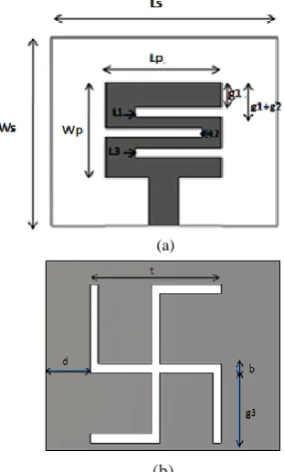
II.GEOMETRY OF PROPOSED ANTENNA The proposed MPA comprises of a slotted radiating patch on top of the substrate and a ground plane which is defected with the help of swastic shape structure on bottom of the substrate. The front and rear outlook of designed antenna is shown in Fig.1(a) and (b).
The rectangular microstrip antenna of length Lp = 12 mm and
width Wp = 8 mm is designed with the epoxy glass FR-4
substrate having dimensions Ls×Ws×Hs= 24×16×1.6 mm3,
relative permittivity, εr = 4.4 and loss tangent, tan δ = 0.0024.
Excitation is made through a microstrip feed line having 50-ohm characteristic line
impedance. Three
g1+g2= 3.4 and g1+g2+1.6 from top of patch are inserted inside
the RMPA. The length of upper and lower open ended slots, L1 and L3 is 8.9 mm and that of middle slot L2 is 10mm. The
ground structure performs as return path for the signal and the slot created in it results in discontinuance in the signal return path and a slow wave effect is produced due to which the resonant frequency shifts down to lower values.
(a)
(b)
Fig.1.Geometrical configuration of the proposed antenna
(a) Front view - Radiating rectangular zigzag shape patch (b) Back view - Swastic shape defected ground structure
[image:2.595.299.554.50.90.2]The position of swastic shaped DGS is adjusted a number of times with hit and trial approach and finally the optimized dimensions of the symmetrical ground slot are taken as length t = 13.4 mm, b = 0.8 mm, d = 4.6 mm and g3 = 6. The lengths, widths and positions of the rectangular open ended slots of the patch and DGS were adjusted carefully for good radiation characteristics. The slots of the swastic shape DGS and the patch play a significant aspect in the favourable excitation of three desired resonating frequency bands. Based on finite integration technique, CST MWS V14.0 software has been used for the examination and optimization of geometrical specifications of the proposed antenna. Transient solver in the main menu contains a parameter sweep option, with the help of which the analytical parameters were regulated precisely after executing a number of experimental repetitions. Finally, for the proposed configuration, the optimal parameters obtained are depicted in Table 1.
TABLE I: Optimal parameters of the proposed microstrip patch antenna
Parameters Value (mm)
Ws 16
Ls 24
L1 8.9
L2 10
L3 8.9
g1 2.1
g2 1.3
g3 6.5
d 4.6
t 13.4
b 1
III. ANTENNASIMULATIONRESULTS
A. Reflection Coefficient
Reflection coefficient, measured in dB, is the difference between forward and reflected power. For perfect matching between the input impedance of the patch antenna and input signal source, a microstrip line feed of 50-Ω was used. A plot between simulated reflection coefficient versus frequency for a rectangular zigzag shape MPA with and without defected ground structure are shown in Fig.2.
Fig.2. Simulated S11 parameter versus frequency plots for
rectangular zigzag MPAwith and without DGS
From Fig.2, it is substantiated that the antenna without DGS shows a return loss of -20.9 dB at the resonating frequency 12.5 GHz along with a return loss less than 10 dB at other two bands. Also, the obtained simulated bandwidth for the resonating band 11.86-12.85 GHz is 981 MHz. When a defected ground structure is inculcated in the design, the antenna structure exhibits a return loss of -14.3 dB, -23 dB and -32 dB at three resonating frequencies 4.55 GHz, 5.8 GHz and 12.4 GHz respectively. The impedance bandwidths of the bands operating at three distinct frequencies having return loss below 10dB are about 100 MHz (4.5-4.6 GHz) (for C-band applications), 110 MHz (5.71–5.82 GHz) (for IEEE 802.11a WLAN band applications) and 1.64 GHz (11.9–13.6 GHz) (for C-band applications). The perfect gaps between three slots of the patch and DGS play a significant role for enhancing the bandwidth and achieving a remarkable return loss.
B.Effect of length of rectangular slots in patch
The effect of length of rectangular slots in patch on the return loss characteristics of proposed antenna is illustrated in Fig.3(a) and (b). Firstly, the length L1 of the rectangular slot
of the MPA is varied from 8.5 to 10.5 which shows the decrease in return loss as the length of the slot increase, as depicted in Fig.3(a). Also, the band at 5.8 GHz shifts towards left with increase in the length. Secondly, the length L2 of the
rectangular slot of the MPA is also varied from 8.5 to 10.5 and the variations are depicted in the Fig.3(b). The best optimized result was with length 10mm to cover the IEEE 802.11a WLAN band and Ku band applications.
[image:2.595.89.245.137.396.2] [image:2.595.313.542.244.349.2](a)
(b)
Fig.3. Variations in resonant frequency and return loss for different
lengths of the proposed antenna (a) L1 and (b) L2
C. Current distribution results
The detailed electromagnetic behaviour of the antenna can be revealed by analysing the field/current distributions above and below the patch. The surface current distribution of the proposed antenna at the resonating frequencies 4.55 GHz, 5.8 GHz and 12.4 GHz, are depicted in Fig.4(a), (b), (c) and (d).
(a)
(b)
(c)
(d)
Fig.4. Current distribution of the proposed antenna at
(a) 4.55 GHz (b) & (c) 5.8 GHz (d) 12.45 GHz
From these figures, it can be observed that firstly the upper and lower open ended slots were strongly responsible for the resonating frequency at 4.55 GHz. Secondly, the current distributions in the middle and lower open ended slots incorporated in the patch and one arm of the swastic shaped DGS were responsible for augmenting the bandwidth of the band resonating at 5.8 GHz. Finally, the current distribution at the end point of the arm and in the middle arm of the swastic shaped DGS clearly justify that present shape of DGS is responsible for the band at 12.4 GHz. Hence all these factors play an important role in covering WLAN standards, C-band and Ku-band applications.
IV. FABRICATIONANDMEASUREMENT
RESULTS
After studying and optimizing the geometrical specifications of the proposed antenna and observing the simulation results in terms of reflection coefficient, effect of length of slots in patch and current distribution, the simulated antenna was fabricated on an Epoxy Glass-FR4 (εr= 4.4,tan δ=0.0024,
thickness h=1.6) dielectric substrate and was examined analytically.
Photolithography technique along with wet etching facility was embraced for fabrication of the proposed antenna and its photograph is presented in Fig.5(a) and (b). The return loss of the fabricated antenna was tested with the help of ENA Series Network Analyzer with operating frequency range of 9KHz-8.5GHz available at Antenna Research Laboratory, Electronics and Communication Engineering Department, Thapar Institute of Engineering and Technology, Patiala, Punjab, India.
(a)
(b)
proposed antenna (a) Front view (b) Rear view
Fig.6 illustrates the measured reflection coefficient/S11
parameter of the proposed antenna. It comes out to be –10.9 dB and -17.7 dB at the resonating frequency of 4.38 GHz and 5.72 respectively. It indicates an impedance bandwidth of 98 MHz at the resonating frequency 4.38 GHz and 100 MHz at 5.72 GHz which is large enough to envelope the required bandwidth for WLAN and C-band applications. The third band in the simulated results operating at 12.4 GHz could not be visualized in the measured results because of the limited frequency range (9kHz-8.5GHz) of ENA Series Network Analyzer.
Fig.6. Measured S11 parameter of the proposed antenna
The slight disagreement in simulated and fabricated results of the proposed antenna could be attributed to fabrication errors, mismatch between SMA connector and feeder, noise and interference.
V.CONCLUSION
A compact triple-band rectangular zigzag MPA with swastic shape DGS has been designed and presented in this paper that covers the WLAN/C-band/Ku-band applications. To improve the impedance bandwidth and return loss values, three rectangular open-ended slots in the zigzag shape and a swastic shape structure in the ground plane were proposed. In this specific antenna configuration, a new shape of defected ground structure is integrated which is basically incumbent for the increase in impedance bandwidth of 12% from 11.998 to 13.636 GHz. The simulated impedance bandwidths of the bands operating at three specific resonating frequencies with return loss below 10-dB are around 1.64 GHz (11.9-13.6 GHz) (for Ku-band applications), 110 MHz (5.71-5.82 GHz) (for IEEE 802.11a WLAN band applications), 100 MHz (4.5-4.6 GHz) (for C-band applications) respectively. It can be concluded from this research paper that the accomplishment of the microstrip antenna rely laboriously on the geometrical dimensionality of the rectangular slots of the patch and the swastic shape DGS been used.
REFERENCES
[1]Balanis CA. Antenna Theory: Analysis and Design. Third Edition. Wiley Interscience. 2005.
[2]Sittironnarit T, Hwang HS, Sadler RA, Hayes GJ. Wide band/dual band package antenna for 5–6 GHz WLAN application. IEEE Trans. on Antennas and Propag. 2004;52(2):610-615.
[3]Li L, Cheung SW, Yuk TI. Dual band antenna with compact radiator for 2.4/5.2/5.8 GHz WLAN applications. IEEE Trans. on Antennas and Propag. 2012;60(12):5924- 5931.
[4]Huang CY, Yu EZ. A slot-monopole antenna for dual-band WLAN applications. IEEE Antennas Wirel. Propag. Lett. 2011;10:500–502. [5]Khalegh A. Dual band meander line antenna for wireless LAN
communication. IEEE Trans. on Antennas and Propag.
2007;55(3):1404–1409.
[6]Kaur J. Development of Dual Band Microstrip Patch Antenna for WLAN /MIMO/ WiMAX/AMSAT/WAVE Applications. Microw. and Opt. Tech. Lett. 2014;56(8):1965-1970.
[7]Kaur J, Khanna R, Kartikeyan MV. Optimization and Development of O-Shaped Triple band Microstrip Patch Antenna for Wireless Communication Applications. IETE Journal of Research.
2014;60(2):95-105.
[8]Patel JM, Patel SK, Thakkar FN. Comparative analysis of S-shaped multiband microstrip patch antenna. Int. J of Adv. Research in Electrical, Electronics and Instrumentation Engg.
2013;2(7):3273–3280.
[9]Kaur J, Khanna R, Kartikeyan MV. Novel Dual Band Microstrip Monopole Antenna with Defected Ground Structure for WLAN /IMT/Bluetooth/WiMAX Applications. Int. J of Microw. and Wirel. Tech. 2014;6(1):93-100.
[10] [10] Chitra RJ, Jayanthi K, Nagaraja V. Design of microstrip slot antenna for WiMAX Application. IEEE Int. Conf. on Comm. and Signal Processing (ICCSP). 2013:645 – 649.
[11] Chakraborty U, Chowdhury SK, Bhatacharjee AK. Frequency tuning and miniaturization of square microstrip antenna embedded with ‘T’-shaped defected ground structure. Microw. and Opt. Tech. Lett.
2013;55(4):869–872.
[12] Chiang KH, Tam KW. Microstrip monopole antenna with enhanced bandwidth using defected ground structure. IEEE Antennas and Wirel. Propag. Lett. 2008;7:532–535.
[13] Ali T, Pathan S, Biradar RC. Multiband, frequency reconfigurable, and metama-terial antennas design techniques: Present and future research directions. Internet Tech Lett. 2018;1:e19.
[14] Ali T, Saadh MAW, Pathan S and Biradar RC. A miniaturized circularly polarized coaxial fed superstrate slot antenna for L-band application.
Internet Tech Lett. 2018;1:e21.
AUTHORSPROFILE
Dr. Jaswinder Kaur received her Ph.D. degree from the Department of Electronics and Communication Engineering, Thapar University, Patiala, Punjab, India in 2014. Her M.Tech. and B.Tech. degrees are from Punjab Technical University, Jalandhar, in 2009 and 2005 respectively. Presently she is working as an Assistant Professor, Department of Electronics and Communication, Thapar Institute of Engg. and Tech., Patiala, Punjab, India. She has several publications in reputed national and international peer reviewed journals/conferences, to her credit. Her research interests include multifrequency microstrip patch antennas
antennas, optimization of antennas using evolutionary algorithms, antennas for biomedical applications etc.
Dr. Rajesh Khanna received his B.Sc. (Engg.) Degree in Electronics and Communication in 1988 from the Regional Engineering College, Kurukshetra, Haryana, India and M.E. degree in 1998 from Indian Institute of Sciences, Bangalore, India. Presently he is working as a Professor, Department of Electronics and Communication, Thapar Institute of Engg. and Tech., Patiala, Punjab, India. He has published several papers in reputed national and international journals/conferences. He has research projects worth Rs. 1.75 crores to his credit. His research interest includes the analysis and design of antennas for wireless communication, MIMO systems, and fractional Fourier transform-based wireless systems, UWB flexible antennas, metamaterial-based structures and microwave absorbers.