Rochester Institute of Technology
RIT Scholar Works
Theses Thesis/Dissertation Collections
12-14-2007
Power reduction techniques for memory elements
Srikanth Katrue
Follow this and additional works at:http://scholarworks.rit.edu/theses
This Thesis is brought to you for free and open access by the Thesis/Dissertation Collections at RIT Scholar Works. It has been accepted for inclusion in Theses by an authorized administrator of RIT Scholar Works. For more information, please [email protected].
Recommended Citation
i
Power Reduction Techniques for Memory Elements
by
Srikanth Katrue
A Thesis Submitted in Partial Fulfillment of the Requirements for the Degree of
Master of Science in Computer Engineering
Supervised by
Dr. Dhireesha Kudithipudi
Department of Computer Engineering
Kate Gleason College of Engineering
Rochester Institute of Technology
Rochester, NY
December 14, 2007
Approved By:
_____________________________________________ ___________ ___
Dr. Dhireesha Kudithipudi
Primary Advisor – R.I.T. Dept. of Computer Engineering
_ __ ___________________________________ _________ _____
Dr. Pratapa V. Reddy
Secondary Advisor – R.I.T. Dept. of Computer Engineering
_____________________________________________ ______________
Dr. Kenneth W. Hsu
ii
Thesis Release Permission Form
Rochester Institute of Technology
Kate Gleason College of Engineering
Title: Power Reduction Techniques for Memory Elements
I, Srikanth Katrue, hereby grant permission to the Wallace Memorial Library to
reproduce my thesis in whole or part.
_________________________________
Srikanth Katrue
_________________________________
iii
Acknowledgements
I am very thankful to my advisor Dr.Dhireesha Kudithipudi for her guidance throughout
my research. Throughout my thesis writing period, she provided me encouragement & lot of
good ideas to keep my motivation focused towards completion of my thesis. I also want to thank
Dr. Kenneth W. Hsu and Dr. Pratapa V. Reddy for being a part of my committee and
encouraging me to complete my thesis.
I am very grateful to my parents, without whose moral support this work would have
never been completed. I am also thankful to the department head, Dr. Andreas Savakis for
motivating me to complete my thesis. I thank the department of Computer Engineering for
providing all the computing facilities and access to needed software. I cannot forget the help and
support of all my friends and colleagues who have helped in every step of the way. Finally I
iv
Abstract
High performance and computational capability in the current generation processors are made
possible by small feature sizes and high device density. To maintain the current drive strength
and control the dynamic power in these processors, simultaneous scaling down of supply and
threshold voltages is performed. High device density and low threshold voltages result in an
increase in the leakage current dissipation. Large on chip caches are integrated onto the current
generation processors which are becoming a major contributor to total leakage power.
In this work, a novel methodology is proposed to minimize the leakage power and dynamic
power. The proposed static power reduction technique, GALEOR (GAted LEakage transistOR),
introduces stacks by placing high threshold voltage transistors and consists of inherent control
logic. The proposed dynamic power reduction technique, adaptive phase tag cache, achieves
power savings through varying tag size for a design window. Testing and verification of the
proposed techniques is performed on a two level cache system.
Power delay squared product is used as a metric to measure the effectiveness of the proposed
techniques. The GALEOR technique achieves 30% reduction when implemented on CMOS
benchmark circuits and an overall leakage savings of 9% when implemented on the two level
cache systems. The proposed dynamic power reduction technique achieves 10% savings when
implemented on individual modules of the two level cache and an overall savings of 3% when
v
Table of Contents
Acknowledgements ... iii
Abstract ... iv
Table of Contents ... v
List of Figures ... viii
List of Tables ... xii
Glossary ... xiii
1 Introduction ... 1
1.1 Impact of Technology Scaling on Power Dissipation ... 1
1.2 Power Dissipation in Microprocessor ... 2
1.3 Thesis Contributions ... 2
1.4 Thesis Organization ... 2
2 Power Dissipation Sources ... 4
2.1 Sources of Dynamic Power Dissipation ... 4
2.1.1 Switching Power ... 4
2.1.2 Short Circuit Power ... 5
2.1.3 Glitching Power ... 6
2.2 Sources of Static Power Dissipation ... 6
2.2.1 Gate Oxide Tunneling Leakage ... 6
2.2.2 Sub-Threshold Leakage ... 8
2.2.3 Reverse-Bias Junction Leakage ... 8
2.2.4 Gate Induced Drain Leakage ... 9
2.2.5 Punch Through Leakage ... 9
2.2.6 Hot Carrier Injection ... 9
2.3 Conclusion ... 9
3 Background Work ... 11
3.1 Static Power Reduction Techniques ... 11
3.1.1 Cache Decay ... 11
3.1.2 Selectively Activated Cache ... 11
3.1.3 Gated Supply Technique ... 12
3.1.4 Leakage Feedback Technique ... 13
3.1.5 Stack Technique ... 14
3.1.6 Sleepy Keeper ... 14
3.2 Dynamic Power Reduction Techniques ... 15
3.2.1 Gate Freezing ... 15
3.2.2 Transistor Sizing ... 16
3.2.3 Guarded Evaluation ... 16
3.2.4 Precomputation Logic ... 17
3.2.5 Dynamically Resizable Cache ... 18
3.3 Conclusion ... 18
vi
4.1 Two Level Cache System ... 20
4.2 CPU Buffer ... 23
4.2.1 Design Specifications ... 23
4.3 Write Buffer ... 23
4.3.1 Design Specifications ... 24
4.4 Translation Look-Aside Buffer ... 24
4.4.1 Instruction TLB Specifications ... 25
4.4.2 Data TLB Specifications ... 26
4.5 Cache ... 27
4.5.1 Level 1 Instruction Cache Specifications ... 27
4.5.2 Level 1 Data Cache Specifications ... 28
4.5.3 Level 2 Unified Cache Specifications ... 29
4.6 Main Memory ... 30
4.7 Conclusion ... 32
5 Proposed Power Reduction Techniques ... 33
5.1 Adaptive Phase Tag Technique ... 33
5.2 GALEOR Technique ... 35
5.3 Leakage Power Analysis in Memory Elements ... 39
5.3.1 ‘D’ Flip – Flop ... 39
5.4 Conclusion ... 40
6 Results ... 42
6.1 Leakage Power Savings in Benchmark Circuits ... 42
6.1.1 Inverter ... 42
6.1.2 Buffer ... 43
6.1.3 Two Input NAND ... 43
6.1.4 Two Input NOR ... 44
6.1.5 Two Input AND ... 45
6.1.6 Two Input OR ... 45
6.1.7 Three Input NAND ... 46
6.1.8 Three Input NOR ... 47
6.1.9 Three Input AND ... 48
6.1.10 Three Input OR ... 49
6.1.11 Two Input XOR ... 50
6.1.12 Two Input XNOR ... 51
6.1.13 ‘D’ Flip – Flop ... 51
6.1.14 ‘D’ Flip – Flop with Reset Enable ... 52
6.1.15 Static Leakage Power Delay Squared Product ... 53
6.2 Leakage Power Savings in the Two Level Cache ... 54
6.3 Dynamic Power Savings in the Memory System ... 55
6.4 Conclusion ... 56
7 Conclusion & Future Work ... 57
vii
8 Bibliography ... 58
9 APPENDIX A ... 61
9.1 CPU Buffer ... 61
9.2 Write Buffer ... 61
9.3 Instruction Translation Look-Aside Buffer ... 61
9.4 Data Translation Look-Aside Buffer ... 62
9.5 Level 1 Instruction Cache ... 63
9.6 Level 1 Data Cache ... 63
9.7 Level 2 Unified Cache ... 64
9.8 Main Memory ... 66
10 APPENDIX B ... 68
10.1 CPU Buffer ... 68
10.2 Write Buffer ... 68
10.3 Instruction Translation Look-Aside Buffer ... 69
10.4 Data Translation Look-Aside Buffer ... 69
10.5 Level 1 Instruction Cache ... 70
10.6 Level 1 Data Cache ... 70
10.7 Level 2 Unified Cache ... 71
10.8 Main Memory ... 72
11 APPENDIX C ... 73
11.1 Schematic of CPU Buffer ... 73
11.2 Schematic of Write Buffer ... 73
11.3 Schematic of Instruction Translation Look-Aside Buffer ... 74
11.4 Schematic of Data Translation Look-Aside Buffer ... 74
11.5 Schematic of Level 1 Instruction Cache ... 74
11.6 Schematic of Level 1 Data Cache ... 74
11.7 Schematic of Level 2 Unified Cache ... 75
11.8 Schematic of Main Memory ... 75
12 APPENDIX D ... 76
12.1 Layout of CPU Buffer ... 76
12.2 Layout of Write Buffer ... 77
12.3 Layout of Instruction Translation Look-Aside Buffer ... 78
12.4 Layout of Data Translation Look-Aside Buffer ... 79
12.5 Layout of Level 1 Instruction Cache ... 80
12.6 Layout of Level 1 Data Cache ... 81
12.7 Layout of Level 2 Unified Cache ... 82
12.8 Layout of Main Memory ... 83
viii
List of Figures
Figure 1.1 - Power Projections by ITRS ... 1
Figure 1.2 - Power Dissipation in Microprocessor ... 2
Figure 2.1 - Components of load capacitance ... 4
Figure 2.2 - Short Circuit Current in Inverter ... 5
Figure 2.3 - Leakage Current Mechanisms ... 6
Figure 2.4 - Components of Tunneling Current... 7
Figure 3.1 - Dual Threshold Voltage Architecture ... 12
Figure 3.2 - Gated Supply Technique ... 13
Figure 3.3 - Leakage Feedback Technique ... 14
Figure 3.4 - Stack Technique ... 14
Figure 3.5 - Sleepy Keeper ... 15
Figure 3.6 - Guarded Evaluation ... 17
Figure 3.7 - Precomputation Logic ... 17
Figure 4.1 - Two Level Cache System ... 19
Figure 4.2 - CPU Buffer... 23
Figure 4.3 - Write Buffer ... 24
Figure 4.4 - Instruction Translation Look-Aside Buffer ... 25
Figure 4.5 - Data Translation Look-Aside Buffer ... 26
Figure 4.6 - Level 1 Instruction Cache ... 28
Figure 4.7 - Level 1 Data Cache ... 29
Figure 4.8 - Level 2 Unified Cache ... 30
ix
Figure 5.1 - Two Way Set Associative Adaptive Phase Tag Cache ... 34
Figure 5.2 - Two Input NAND Gate ... 35
Figure 5.3 - GALEOR Technique Implemented on a Two Input NAND Gate ... 37
Figure 5.4 - Gated Leakage ‘D’ Flip – Flop ... 40
Figure 6.1 - Leakage Power Dissipation in an Inverter ... 42
Figure 6.2 - Leakage Power Dissipation in a Buffer ... 43
Figure 6.3 - Leakage Power Dissipation in a Two Input NAND Gate ... 44
Figure 6.4 - Leakage Power Dissipation in a Two Input NOR Gate ... 44
Figure 6.5 - Leakage Power Dissipation in a Two Input AND Gate ... 45
Figure 6.6 - Leakage Power Dissipation in a Two Input OR Gate ... 46
Figure 6.7 - Leakage Power Dissipation in a Three Input NAND Gate ... 47
Figure 6.8 - Leakage Power Dissipation in a Three Input NOR Gate ... 48
Figure 6.9 - Leakage Power Dissipation in a Three Input AND Gate ... 49
Figure 6.10 - Leakage Power Dissipation in a Three Input OR Gate ... 50
Figure 6.11 - Leakage Power Dissipation in a Two Input XOR Gate ... 50
Figure 6.12 - Leakage Power Dissipation in a Two Input XNOR Gate ... 51
Figure 6.13 - Leakage Power Dissipation in a ‘D’ Flip – Flop ... 52
Figure 6.14 - Leakage Power Dissipation in a ‘D’ Flip – Flop with Reset Enable ... 53
Figure 6.15 - Static Leakage Power Savings in the Benchmark Circuits ... 53
Figure 6.16 - Leakage Power Delay Squared Product Savings in Buffer’s & TLB’s……54
Figure 6.17 - Leakage Power Delay Squared Product Savings in Level 1, Level 2 Caches & Main Memory..………54
x
Figure 6.20 - % Dynamic Power Delay Squared Product Savings in Memory System….55
Figure 10.1 - Functional Simulation of CPU Buffer... 68
Figure 10.2 - Functional Simulation of Write Buffer ... 68
Figure 10.3 - Functional Simulation of Instruction TLB ... 69
Figure 10.4 - Functional Simulation of Data TLB ... 69
Figure 10.5 - Functional Simulation of Level 1 Instruction Cache ... 70
Figure 10.6 - Functional Simulation of Level 1 Data Cache ... 70
Figure 10.7 - Functional Simulation of Level 2 Unified Cache ... 71
Figure 10.8 - Functional Simulation of Main Memory ... 72
Figure 11.1 - Schematic of CPU Buffer... 73
Figure 11.2 - Schematic of Write Buffer ... 73
Figure 11.3 - Schematic of Instruction TLB ... 74
Figure 11.4 - Schematic of Data TLB ... 74
Figure 11.5 - Schematic of Level 1 Instruction Cache ... 74
Figure 11.6 - Schematic of Level 1 Data Cache ... 74
Figure 11.7 - Schematic of Level 2 Unified Cache ... 75
Figure 11.8 - Schematic of Main Memory... 75
Figure 12.1 - Layout of CPU Buffer ... 76
Figure 12.2 - Layout of Write Buffer... 77
Figure 12.3 - Layout of Instruction TLB ... 78
Figure 12.4 - Layout of Data TLB ... 79
Figure 12.5 - Layout of Level 1 Instruction Cache ... 80
Figure 12.6 - Layout of Level 1 Data Cache ... 81
xi
xii
List of Tables
Table 5.1 - Allocation of Tag bits based on the Hit Ratio ... 34
Table 5.2 - Leakage Current in Two Input NAND gate ... 36
Table 5.3 - Leakage Current in Two Input Gated Leakage Transistor NAND gate ... 39
Table 5.4 – Stacks added in a Gated Leakage D Flip - Flop ... 40
Table 9.1 – Functional Pin Description of CPU Buffer ... 60
Table 9.2 – Functional Pin Description of Write Buffer ... 60
Table 9.3 – Functional Pin Description of Instruction TLB ... 60
Table 9.4 – Functional Pin Description of Data TLB ... 61
Table 9.5 – Functional Pin Description of Level 1 Instruction Cache... 62
Table 9.6 – Functional Pin Description of Level 1 Data Cache ... 62
Table 9.7 – Functional Pin Description of Level 2 Unified Cache ... 63
xiii
Glossary
NMOS N – Channel Metal Oxide Semi Conductor
PMOS P – Channel Metal Oxide Semi Conductor
CMOS Complementary Metal Oxide Semiconductor.
ITRS International Technology Roadmap for Semiconductors
ITLB Instruction Translation Look-Aside Buffer
DTLB Data Translation Look-Aside Buffer
ICACHE Instruction Cache
DCACHE Data Cache
VPN Virtual Page Number
GALEOR Gated Leakage Transistor
1
Chapter 1
Introduction
Increase in the transistor speed and number of transistors result in high
performance in the current generation processors. The performance improvements have been
accompanied by an increase in the power dissipation. High power dissipation systems increase
cost of cooling and reduce the system reliability.
1.1Impact of Technology Scaling on Power Dissipation
CMOS technology has been scaled down from 1µm to 45nm over the last decade. Technology
scaling reduces the gate oxide thickness and the gate length thereby increasing the transistor
density and also reduces the delay. Reduced gate lengths result in an increase in the leakage
power dissipation. Increased transistor densities result in an increase in the power dissipation per
unit area thereby creating hotspots. In the Figure 1.1, the static power dissipation is expected to
[image:15.612.119.498.431.696.2]equal the dynamic power dissipation by the year 2007.
Scaling down the supply voltage reduces the switching power dissipation. Threshold voltage is
simultaneously scaled down along with the supply voltage
Scaling down the threshold voltage significantly increases the leakage power dissipation.
1.2Power Dissipation in Microp
FIGURE
Caches consume almost 50% of the total leakage power dissipated. Leakage power dissipation in
caches continue to increase due to the increase in the transistor density.
1.3Thesis Contributions
In this thesis we developed a working model of a two level cache
bed for running the dynamic and static power simulations. We proposed dynamic and static
power reduction techniques with minimal area and performance overhead.
1.4Thesis Organization
Thesis is organized as follows. Chapter 2 deals with the different sources of power dissipation.
Chapter 3 outlines the existing power reduction techniques for minimizing dynamic and leakage CPU 31% Other 5% Clock 6% Control 2
Scaling down the supply voltage reduces the switching power dissipation. Threshold voltage is
simultaneously scaled down along with the supply voltage to improve transistor switching speed.
Scaling down the threshold voltage significantly increases the leakage power dissipation.
Power Dissipation in Microprocessor
FIGURE 1.2: Power Dissipation in Microprocessor
Caches consume almost 50% of the total leakage power dissipated. Leakage power dissipation in
caches continue to increase due to the increase in the transistor density.
In this thesis we developed a working model of a two level cache system which is used as a test
bed for running the dynamic and static power simulations. We proposed dynamic and static
power reduction techniques with minimal area and performance overhead.
Thesis is organized as follows. Chapter 2 deals with the different sources of power dissipation.
Chapter 3 outlines the existing power reduction techniques for minimizing dynamic and leakage D Cache 31% ITLB 7% DTLB 9% CPU 31% Control 5% Write Buffer 6%
Scaling down the supply voltage reduces the switching power dissipation. Threshold voltage is
to improve transistor switching speed.
Scaling down the threshold voltage significantly increases the leakage power dissipation.
Caches consume almost 50% of the total leakage power dissipated. Leakage power dissipation in
system which is used as a test
bed for running the dynamic and static power simulations. We proposed dynamic and static
Thesis is organized as follows. Chapter 2 deals with the different sources of power dissipation.
3
power. Chapter 4 discusses the two level cache system and the functionality of each of the sub
modules. In chapter 5 proposed power reduction techniques were discussed. Chapter 6 presents
the results obtained by implementing the power reduction techniques on standard gates and two
level cache system. Finally chapter 7 presents conclusions and suggestions for future research
4
Chapter 2
Power Dissipation Sources
Speed and area are the main objectives in designing high end systems and portable
electronic devices. However design of low power systems has become a prime concern in the
current generation processors. Two principal sources of power dissipation in modern processors
are dynamic power and static leakage power.
2.1 Sources of Dynamic Power Dissipation
2.1.1 Switching Power
Switching power dissipation in a circuit results from charging/discharging the output load
capacitance to supply/ground voltage. The power dissipation depends on supply voltage, output
load capacitance and frequency of output transitions [2]. The output load capacitance is the sum
of gate to drain capacitance, diffusion capacitance and wiring capacitance [2]. Switching power
is expressed in equation 2.1 as follows
= →∗ ∗ ∗ ∗ (2.1)
where is the sum of gate, junction and interconnect capacitances as shown in Figure 2.1,
is the supply voltage, is the output logic swing, is the operating frequency and is the
activity factor. We can clearly observe that the switching power has linear dependence on load
capacitance, frequency of input transitions and a quadratic dependence on supply voltage.
5
2.1.2 Short Circuit Power
Short circuit power dissipation results due to the current flowing from supply to ground during
input signal transitions. Consider an inverter circuit shown in the Figure 2.2, when the input
voltage is between vtn and vdd - |vtp| (vtn is the NMOS threshold voltage and vtp is the PMOS
threshold voltage) and output voltage is between ground and supply voltages, a conductive path
exists from supply to ground allowing the short circuit current to flow [3]. The equation for short
circuit power is given by the equation 2.2
Psc = ∗ ∗ ∗ − 2 ∗ ∗ ∗ (2.2)
where is the input transition time, is the threshold voltage of the transistors, is the
effective trans-conductance parameter of the logic gate, is the supply voltage, f is the
frequency of operation and α is the switching factor. To minimize short circuit current it is
desirable to have equal input and output rise/fall times since input rise/fall time of one gate is the
output rise/fall time of other gate. To eliminate short circuit power completely the supply voltage
is made smaller than the sum of threshold voltages of NMOS and PMOS transistors [2]. The
Figure 2.2 below shows flow of short circuit current in an inverter and peak of short circuit
current occurs when both NMOS and PMOS devices are turned ON.
6
2.1.3 Glitching Power
Glitching power dissipation occurs due to mismatch in input signal path lengths in a network [5].
Glitch power is minimized when the width of the glitch is made smaller than the delay of the
gate and also when all the inputs to a gate arrive simultaneously [4].
2.2 Sources of Static Power Dissipation
Static leakage power dissipation occurs due to the current flowing through the transistors in the
idle state. Leakage power dissipation depends on threshold voltage, gate size and oxide
thickness.
FIGURE 2.3: Leakage Current Mechanisms [6]
In the Figure 2.3 above is the reverse bias junction leakage, is subthreshold leakage, is
gate oxide tunneling leakage, is current due to hot carrier injection, is gate induced drain
leakage and is punch through current. Each of the currents is discussed below in detail.
2.2.1 Gate Oxide Tunneling Leakage
Scaling down the gate oxide thickness increases electric field across the gate. The high electric
field causes electrons to tunnel from gate to substrate and substrate to gate resulting in gate oxide
leakage current [7, 8]. Two possible mechanisms causing this tunneling phenomenon are
Fowler-Nordheim tunneling and direct tunneling [6]. Fowler-Fowler-Nordheim tunneling results from the
7
barrier [6]. Thickness of the barrier, barrier height and structure of the barrier determine the
tunneling probability of an electron. The current density in the FN tunneling is given by the
equation 2.3
!" = $%∗&'()
∗*)∗+∗,'(∗ exp 0−∗√∗2∗,'( % )3
∗+∗$∗&'( 4 (2.3)
where 567 is the field across the oxide 867 is the barrier height for electrons in the conduction
band, m is the effective mass of electron in the conduction band of silicon, h is Planck’s constant.
In direct tunneling electrons from the silicon surface tunnel to the gate through the forbidden
energy gap in silicon dioxide [6]. The current density in the direct tunneling mechanism is given
by the equation
9: = ; ∗ 567 ∗ exp <−
=>?@?B'(A'(C% )3 D
&'( E (2.4)
Where ; = $%
∗*)∗+∗,'(,F =∗√∗2∗,'( % )3
∗+∗$ , q is the electron charge.
Gate oxide tunneling current shown in the Figure 2.4 below comprises of leakage current
through the gate to the source and drain overlap regions (Igso and Igdo), gate to channel leakage
current (Igc) and gate to substrate leakage current (Igb) [9].
8
2.2.2 Sub-threshold Leakage
Sub-threshold leakage current flows between the source and drain of an MOS transistor when the
gate voltage is less than the threshold voltage [4]. Sub-threshold conduction is given by the
equation 2.5
IHI = μL∗ CLN∗OP ∗ m − 1 ∗ S∗ T
UAVW – AYZ [
\∗AY ∗ ]1 − T^A_WAY ` (2.5)
where
m = 1 + bcd
bef
is the sub-threshold swing co-efficient, g2 is capacitance of the depletion layer, g67 is the
capacitance of the oxide layer, h6 is the mobility, + is the threshold voltage, is the gate to
source voltage, is the drain to source voltage and = i:
$ is the thermal voltage. The inverse
slope of IHI versus characteristic of a MOS device is called sub-threshold slope and is given
by j= 2.32∗m∗:
$ [4]. Sub-threshold slope indicates how effectively a transistor can be turned
off when gate voltage is below the threshold voltage [6].
Reverse biasing substrate to source junction [10, 11] increases threshold voltage thereby
reducing the sub-threshold current. In short channel devices, the depleted source and drain
regions interact with each other reducing the potential barrier [6], thereby reducing the threshold
voltage which increases the sub-threshold leakage current.
2.2.3 Reverse-Bias Junction Leakage
P-N junctions between the source/drain and substrate are reverse biased allowing a small amount
of reverse bias leakage current to flow across the junctions [6]. Reverse bias leakage increases
with high electric field strengths [11]. The magnitude of the leakage current depends on the area
9
current. Reduction in the substrate doping near diffusion regions reduces the reverse bias
junction leakage [6].
2.2.4 Gate Induced Drain Leakage
This leakage occurs when potential of the channel region is almost the same as potential of
substrate [6]. Suppose a negative gate bias is applied to an NMOS device, the drain region
underneath the gate will be depleted of any electrons [6]. Increase in the electric field results in
avalanche breakdown generating minority carriers [6]. These minority carriers are swept from
the channel to the substrate resulting in gate induced drain leakage current [12].
2.2.5 Punch through Leakage
In short channel devices, source and drain regions extend into channel reducing the effective
length of channel [12]. When the reverse bias voltage across the drain-substrate and
source-substrate junctions is increased, the diffusion regions merge with each other resulting in large
leakage current flowing between drain and source junctions [6]. This leakage current is called
punch through leakage current [12].
2.2.6 Hot Carrier Injection
High electric fields near the channel-oxide interface causes electrons or holes to overcome the
potential barrier and enter oxide layer causing hot carrier effect [11]. These trapped electrons or
holes in the oxide layer change the threshold voltage thereby affecting the sub-threshold leakage
current [11]. Scaling down the supply voltage with the device dimensions controls the leakage
current.
2.3 Conclusion
Scaling down the transistor channel lengths below 45 nm in deep sub-micron technology results
10
threshold voltages as low as 0.22V result in an increase in the leakage power dissipation.
However, controlling threshold voltages of the transistors is difficult in the sub-micron
technologies. High computational capability is achieved by switching signals faster thereby
increasing dynamic switching power. Hence the issues of static leakage power and dynamic
power continue to play an important role in the processor design. Chapter 3 presents various state
11
Chapter 3
Background Work
This chapter outlines the various state of art techniques for reducing both static leakage
power and dynamic power. In the current literature, techniques were proposed to reduce dynamic
and static leakage power at different levels of abstraction. In the following subsections
architectural and circuit level techniques for power reduction will be discussed.
3.1Static Power Reduction Techniques
3.1.1 Cache Decay
This technique uses an assumption that caches tend to store items that will not be referenced in
future. Savings in the leakage power and performance overhead can be achieved by placing the
unused cache items in the deep sleep mode before being evicted from cache [13]. Time based
leakage control technique is used to turn OFF the unused cache items. In this technique unused
lines are observed over a period of time and when it is likely that no further accesses are made,
the cache lines are put to sleep reducing power dissipation [13]. Turning off the line prematurely
would result in a miss and increase the access time while turning off the line late would result in
an increase in the leakage power dissipation [13]. Small interval lengths increase the leakage
power dissipation [13]. An adaptive variant of the time based leakage control policy initially
chooses small decay time interval, length of the interval is varied based on number of unused
cache lines [13]. Probable improvements can be made by dynamically selecting the time interval
based on the level of parallelism between the instructions and also in the direction of using
probabilistic methods to predict the time interval size.
3.1.2 Selectively activated cache
In this technique the cache is divided into blocks and threshold voltage of the each block is
12
awake while the rest of the blocks are put to sleep. Dual threshold voltage technique [15] as
shown in the Figure 3.1 is used to vary threshold voltages of the individual blocks. During active
mode the SRAM circuit is connected to supply and ground rails [15]. During the sleep mode
threshold voltages of the internal transistors are increased due to substrate bias effect, thereby
reducing the static leakage current [15]. A prediction table keeps track of the addresses of active
blocks in the cache [14]. Special register called previous block address register stores the address
of the recently accessed cache block. When the address of the currently accessed block matches
the address in the previous block address register, the corresponding line is awaken and address
of the block is added to the prediction table [14]. Increasing the entries in the prediction table
achieves high performance thereby increasing the leakage power [14]. Block prediction [14] can
be made based on the type of instruction thereby reducing the delay. Improvements can be
sought in the direction of finding a better algorithm to add unused entries to prediction table.
FIGURE 3.1:Dual Threshold Voltage Architecture [14]
3.1.3 Gated-Vdd Technique
In this technique supply voltage is turned OFF to minimize power dissipation in unused parts of
13
turned ON in the active parts of the circuit and turned OFF in the unused parts of the circuit.
Reduction in the leakage power is achieved due to the stacking effect introduced by the
additional control transistors [17]. Implementation of this technique on the SRAM cell is shown
in the Figure 3.2 where the gated control transistor is placed between ground rail and circuit
[image:27.612.209.400.220.377.2]reducing the standby leakage power.
FIGURE 3.2: Gated Supply Technique [17]
The gated-Vdd control NMOS transistor in Figure 3.2 must be made sufficiently wide to maintain
the speed. Sharing a single gated control transistor among multiple circuit blocks requires careful
sizing of the gated-Vdd control transistor [17].
3.1.4 Leakage Feedback Technique
In this technique the state of circuit is preserved by re-circulating the data through the circuit
during the standby mode [18]. In the Figure 3.3 P1 and N1 transistors are sleep devices and P2
and N2 transistors are helper sleep devices having high threshold voltage [18]. During the active
mode both the sleep and helper sleep devices are turned on allowing the circuit to
charge/discharge to supply/ground voltages [18]. During the standby state either one of the
helper sleep devices is turned on to preserve state of the circuit. Glitches in the input signal
14
FIGURE 3.3: Leakage Feedback Technique [18]
3.1.5 Stack Technique
In this technique each transistor is split into two transistors as shown in the Figure 3.4. Consider
an inverter circuit, when the input to circuit is a ground voltage the PMOS transistor is turned
ON while both the NMOS transistors are turned OFF. Leakage current flowing through the
NMOS transistor stack reduces due to the increase in the source to substrate voltage in the top
NMOS transistor and also due to an increase in the drain to source voltage in the bottom NMOS
transistor [19]. This technique introduces considerable performance overhead due to the stacking
of transistors.
FIGURE 3.4: Stack Technique [19]
3.1.6 Sleepy Keeper
In this technique low threshold NMOS transistor is placed in parallel to a high threshold voltage
15
placed in parallel to a high threshold voltage NMOS sleep transistor as shown in the Figure 3.5.
During the active mode, both the sleep devices and additional MOS transistors are turned on to
improve circuit performance [20]. During the standby mode, the sleep transistors are turned off
thereby reducing the leakage current [20]. Additional MOS transistors preserve state of the
circuit during idle mode. This technique reduces the output drive strength based on the fact that
PMOS device passes a weak zero and NMOS device passes a weak 1, resulting in a delay
[image:29.612.229.389.271.436.2]increase.
FIGURE 3.5: Sleepy Keeper [20]
3.2Dynamic Power Reduction Techniques
3.2.1 Gate Freezing
This technique involves automatic circuit transformation for reducing the glitch power [21]. The
gates with high spurious switching activity are replaced with functionally equivalent gates which
are insensitive to input signal transitions by asserting a control signal [21]. Small subset of gates
is used to generate the control signal. Asserting the control signal low, ensures gate is insensitive
to input signal transitions [21]. Glitches are eliminated by keeping control signal low to stabilize
16
[21]. Gates are clustered according to their arrival time to reduce the wiring overhead. This
technique increases area overhead by the addition of the control logic circuitry.
3.2.2 Transistor Sizing
This technique achieves savings in power and delay by optimal sizing of transistors in critical
and non critical paths [22]. Delay tolerance indicates the possible worst case delay for each
transistor in the circuit. The transistor sizes in non-critical paths are scaled down without
affecting the tolerable delay of each transistor [22]. Reduction in the delay is achieved by
searching for the most critical path instead of ‘N’ number of critical paths [22] to size devices for
optimal performance. The critical path search is repeated till the user defined number of
iterations and user defined improvement ratio are reached [22]. Transistor sizing in non-critical
paths gives rise to new critical paths in the circuit. Most of the circuits in real time have more
critical paths, where the technique achieves less savings in the dissipated power.
3.2.3 Guarded Evaluation
The technique is used to identify unused parts of the circuit that can be turned off without
affecting the overall delay of the circuit [23]. Latches are used as transition barriers. When the
latch is enabled, inputs to the latches are passed to the circuits to perform useful computation
[23]. When enable goes low latches retain their previous state preventing the inputs from
reaching the circuit. In the Figure 3.6, guard logic is placed before the combinational circuit to
selectively turn off the inputs to the parts of the combinational circuit when not needed.
Performance improvement and reduction in the area are achieved by using existing signals to
17
F
Combinational Logic
OUT IN
S Bar Guard Latches
IN F
Combinational Logic
OUT
FIGURE 3.6: Guarded Evaluation [23]
3.2.4 Precomputation Logic
The technique selectively computes the output values of circuit one clock cycle before they are
required [23]. The precomputed values reduce switching in the subsequent cycles. Output from
the precomputation logic is used to enable/disable registers that feed inputs to combinational
circuits [23]. Precomputation logic size is kept under control since increase in the size of
precomputation logic could dissipate more power that would offset savings achieved by blocking
the switching activity [23]. In the Figure 3.7 below output from the precomputation logic g1 and
g2, turns on/off the latch R2 to allow/block the inputs reaching the combinational block A.
18
3.2.5 Dynamically resizable cache
Savings in the dynamic power dissipation is achieved by resizing the cache to reduce the
switching activity in the circuits. Minimum size the cache can assume is called size-bound [16].
Miss-bound allows cache to adapt to working set and bound miss rate in each interval [16]. An
adaptive mechanism monitors cache in fixed time intervals called sense intervals [16]. Miss
counter counts number of misses in each sense interval. At the end of each sense interval, the
cache upsizes/downsizes, depending on whether the miss counter is lower/higher than the
miss-bound [16]. Inaccurate estimation of the cache size will result in redundant accesses to higher
levels of memory thereby increasing delay penalty and dynamic power dissipation [16].
Mechanisms to detect optimal sense interval length and repeated sizing are required to reduce
unnecessary accesses to memory. Improvements would be in finding a mechanism for
calculating the time between the application phases that would be long enough to offset the
resizing overhead [16].
3.3Conclusion
Dynamic power reduction techniques explained above increase area overhead and possibly
introduce new critical paths by adding additional control logic to reduce power. Static power
reduction techniques introduce area and performance overhead by adding high threshold voltage
transistors and increasing the number of transistors in the stack to reduce leakage power during
standby state. Chapter 4 explains modules present in the two level cache model, which serves as
19
Chapter 4
System Level Design
Multiple level caches tend to improve system performance by reducing the miss
rate while contributing significantly towards power dissipation. A two level cache system
consisting of a level 1 split cache and level 2 unified cache was designed as a test bed for a two
way superscalar architecture. Overview on the two level cache system and functionality of each
of the cache sub-modules are discussed below in detail.
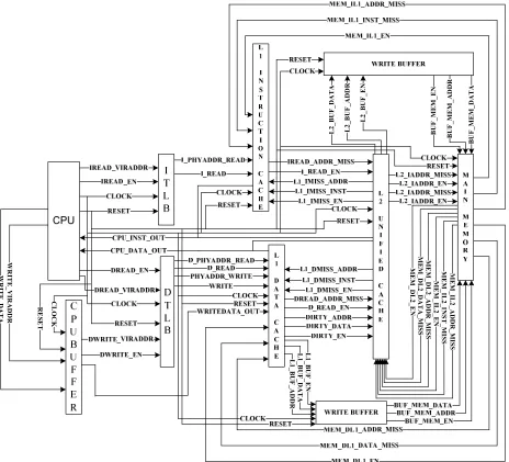
[image:33.612.78.542.253.674.2]L 1 _ B U F _ A D D R L 1 _ B U F _ D A T A L 1 _ B U F _ E M E M _ IL 2 _ A D D R _ M IS S M E M _ IL 2 _ I S T _ M IS S M E M _ IL 2 _ E M E M _ D L 2 _ A D D R _ M IS S M E M _ D L 2 _ D A T A _ M IS S M E M _ D L 2 _ E B U F _ M E M _ D A T A L 2 _ B U F _ D A T A L 2 _ B U F _ A D D R L 2 _ B U F _ E B U F _ M E M _ A D D R B U F _ M E M _ E WR IT E _ V IR A D D R WR IT E _ D A T A C L O C K R E S E T
20
4.1Two Level Cache System
The two level cache system shown in the Figure 4.1 consists of sub-modules like CPU buffer,
instruction translation look-aside buffer, data translation look-aside buffer, level 1 instruction
cache, level 1 data cache, level 2 unified cache and write buffer. Outputs of the sub-modules are
valid during the positive edge of clock and when the reset is low.
Virtual addresses IREAD_VIRADDR, DREAD_VIRADDR of the instructions and data
requested by the CPU are sent to instruction TLB and data TLB. Virtual address
WRITE_VIRADDR of the data sent by CPU is stored in the CPU buffer. CPU buffer stores the
address WRITE_VIRADDR and the data WRITE_DATA to reduce the CPU delay overhead,
and the output buffered address DWRITE_VIRADDR and data WRITEDATA_OUT are sent to
data TLB and level 1 data cache respectively.
When the instruction TLB is enabled IREAD_EN during a cache read, virtual address
IREAD_VIRADDR is translated to physical address I_PHYADDR_READ. During a cache read,
when the data TLB is enabled DREAD_EN the virtual address DREAD_VIRADDR is translated
to the physical address D_PHYADDR_READ. When the data TLB is enabled WRITE_EN
during a cache write, virtual address DWRITE_VIRADDR is translated to physical address
PHYADDR_WRITE.
Set associative level 1 instruction cache is divided into sets. Each set is divided into lines and
each line is divided into blocks. Each block consists of valid tag, dirty tag, address tag, data tag
and LRU tag. Valid tag indicates if the address location in the cache contains valid
data/instruction. When dirty tag is set, the data in the cache location is missing from main
21
instruction. Data tag provides the actual data stored in the cache. During a cache miss, write-back
with write-allocate policy is used.
The Level 1 instruction cache is enabled I_READ to find an input address I_PHYADDR_READ
match stored in the cache. When an address match occurs in Level 1 instruction cache, the
instruction CPU_INST_OUT is sent to the CPU. When there is no matching address in the level
1 instruction cache, address of the missed instruction IREAD_ADDR_MISS is sent to level 2
unified cache.
Level 1 data cache is enabled D_READ to find an input address D_PHYADDR_READ match
stored in the cache. When an address match occurs in Level 1 data cache, the data
CPU_DATA_OUT is sent to CPU. When there is no matching address in the level 1 data cache,
address of the missed data DREAD_ADDR_MISS is sent to level 2 unified cache. During a
write to the level 1 data cache, the write data WRITEDATA_OUT is written to the address
location PHYADDR_WRITE when the dirty flag is reset. When the dirty flag is set, the data
DIRTY_DATA in the location PHYADDR_WRITE is written to the address DIRTY_ADDR
location in level 2 cache and also to the write buffer location L1_BUF_ADDR.
During a level 1 instruction cache miss, level 2 unified cache is enabled I_READ_EN to find
miss address IREAD_ADDR_MISS match stored in the level 2 unified cache. When the address
match occurs in the level 2 unified cache, the data CPU_INST_OUT is sent to the CPU and also
to the location L1_IMISS_ADDR in the level 1 instruction cache by enabling L1_IMISS_EN
control signal. When there is no match, the miss address L2_IADDR_MISS is sent to the main
22
Unified level 2 cache is enabled D_READ_EN to find miss data address DREAD_ADDR_MISS
match stored in the level 2 unified cache. When the address match occurs, the data
CPU_DATA_OUT is sent to CPU and also to the location L1_DMISS_ADDR in the level 1 data
cache by enabling L1_DMISS_EN. During a miss in the level 2 unified cache, the address
L2_DADDR_MISS of the missed data is sent to main memory. The dirty data DIRTY_DATA
sent by level 1 data cache is stored in the location DIRTY_ADDR when the control signal
DIRTY_EN is enabled and the dirty tag is reset. When the dirty tag is set, the data from the
location DIRTY_ADDR is written to the location L2_BUF_ADDR in write buffer.
Write buffer stores the data L1_BUF_DATA sent by the level 1 data cache in the location
L1_BUF_ADDR. Data L2_BUF_DATA sent by the level 2 unified cache is stored in the
location L2_BUF_ADDR. When main memory is idle, the data L1_M_BUF_DATA sent by the
write buffer is written to the location L1_M_BUF_ADDR. Data L2_M_BUF_DATA sent by the
write buffer is stored in the location L2_M_BUF_ADDR.
Main memory looks-up the miss instruction L2_IADDR_MISS request sent by the level 2
unified cache. Miss address found in the main memory is sent to the location
MEM_IL1_ADDR_MISS in the level 1 instruction cache and also sent to the location
MEM_IL2_ADDR_MISS in the level 2 unified cache. Data in the miss address location in main
memory is sent to MEM_IL1_INST_MISS in the level 1 instruction cache and also sent to
MEM_IL2_INST_MISS in the level 2 unified cache. Miss data request L2_DADDR_MISS sent
by the level 2 instruction cache is looked-up by main memory. Miss address location found in
the main memory is sent to location MEM_DL1_ADDR_MISS in the level 1 data cache and also
23
address location in the main memory is sent to MEM_DL1_DATA_MISS and also sent to
address MEM_DL2_DATA_MISS.
4.2CPU Buffer
This module buffers the data sent by the CPU. When CPU buffer gets full, buffered data is
written to the data cache. To minimize the delay in writing buffered data to data cache, size of
the buffer is reduced. Data coherency between the CPU buffer and data cache need to be
maintained, to prevent false data from being read by CPU. To prevent an incorrect update in the
data cache contents, size of the buffer is matched with the block size of the data cache.
4.2.1 Design Specifications
Size of each entry in buffer = noopTqq rstq + ontn rstq = 32 + 32 = 64 rstq Total number of entries in buffer = 128
Total size of buffer = qswT x Tngℎ Tztp{ ∗ txtn| z}~rTp x TztpsTq sz r}Tp
= 64 ∗ 128 = 1F
A model CPU buffer is shown in the Figure 4.2. Table I in Appendix I explains functionality of
each of the input and output pins in the model CPU buffer.
CPU BUFFER addr_in1[31:0]
addr_in2[31:0]
write1 data_in2[31:0] data_in1[31:0]
write2 clock
reset
addr_out1[31:0] addr_out2[31:0]
accept1 data_out2[31:0] data_out1[31:0]
accept2 en1 en2
FIGURE 4.2:CPU Buffer
4.3Write Buffer
This module temporarily stores the data from the cache, allowing the cache to serve the read
24
main memory for a free time slot, during which data stored in the write buffer is written to main
memory. Write buffer includes a logic that checks whether a read address matches any of the
addresses waiting in the write buffer. When a match is detected, data is read back from the buffer
instead of the main memory reducing the data access time. FIFO policy is used to send and
retrieve information from the write buffer.
4.3.1 Design Specifications
Size of each entry in write buffer = noopTqq rstq + ontn rstq = 32 + 512 = 544 rstq Total number of entries in buffer = 128
Total size of buffer = qswT x Tngℎ Tztp{ ∗ txtn| z}~rTp x TztpsTq sz r}Tp
= 544 ∗ 128 ≈ 8F
A model write buffer is shown in the Figure 4.3. Table II in Appendix I explains functionality of
each of the input and output pins in the model write buffer.
FIGURE 4.3: Write Buffer
4.4Translation Look-Aside Buffer
The TLB is used to improve speed of virtual address translation by storing the addresses of
recently accessed page table entries, thereby reducing instruction/data accesses to main memory.
During a virtual memory access, CPU searches the TLB for the virtual page number of the page
being accessed, operation known as TLB look-up. When the TLB entry is found with a matching
25
by the cache. When a miss occurs, operation of CPU is suspended until a new value is loaded
from the main memory into the TLB entry where miss occurred.
4.4.1 ITLB Design Specifications
The instruction TLB is a 4 way set associative cache.
Total number of sets in instruction TLB = 4
Total size of instruction TLB = 16 F
Size of each set in the instruction TLB = 6 6 6 :=
6 2 6 6 := = F = 4 F
Size of each block in the instruction TLB = physical address bits + (valid bits+ virtual address
bits)*offset value = 22 + (1+21)16 = 374
Total number of lines in each set = 6 + + 6 :=
6 + 6m + 6 :==
∗∗
≈ 87
Total offset bits = |zxqTt n|}T = |z16 = 4
Total index bits = |ztxtn| z}~rTp x |szTq sz Tngℎ qTt = |z87 ≈ 7
Total number of tag bits = txtn| noopTqq rstq − txtn| xqTt rstq + txtn| szoT rstq
= 32 − 4 + 7 = 21
A model instruction translation look-aside buffer is shown in the Figure 4.4. Table III in
Appendix I explains functionality of each of the input and output pins in the model instruction
translation look-aside buffer.
INSTRUCTION TRANSLATION LOOK ASIDE BUFFER mem_tlb_en1 mem_tlb_en2 mem_tlb_viraddr1[31:0] mem_tlb_viraddr2[31:0] vir_addr1[31:0] vir_addr2[31:0] vir_en1 vir_en2 clock reset phy_addr1[31:0] phy_addr2[31:0] hit_1 hit_2 tlb_mem_en1 tlb_mem_en2 tlb_mem_viraddr1[31:0] tlb_mem_viraddr2[31:0] physaddr1_en1 physaddr2_en2
26
4.4.2 DTLB Design Specifications
The data TLB is a 4 way set associative cache.
Total number of sets in data TLB = 4
Total size of data TLB = 64 F
Size of each set in the data TLB = 6 6 :=
6 2 6 :==
F = 16 F
Size of each block in the data TLB = physical address bits + (valid bits + virtual address
bits)*offset value = 20 + (1+19)*16 = 340
Total number of lines in each set = 6 + + 6 :=
6 + 6m + 6 :==
∗∗
≈ 385
Total offset bits = |zxqTt n|}T = |z16 = 4
Total index bits = |ztxtn| z}~rTp x |szTq sz Tngℎ qTt = |z385 ≈ 9
Total number of tag bits = txtn| noopTqq rstq − txtn| xqTt rstq + txtn| szoT rstq
= 32 − 4 + 9 = 19
A model data translation look-aside buffer is shown in the Figure 4.5. Table IV in Appendix I
explains functionality of each of the input and output pins in the model data translation
look-aside buffer.
27
4.5Cache
Cache is a high speed buffer where frequently accessed instructions or data can be temporarily
stored. Each entry in the cache consists of address tag, data and a valid bit. Address tag stores the
location of the entry, data field has the information requested by the CPU and the valid bit
indicates whether the entry is valid. When data requested by the CPU is found in the cache, hit
occurs. During an address miss an address request is sent to a high level memory. Principle used
in cache for storing data is locality of reference. Principle of locality states that the currently
accessed data and its logically adjacent data are more likely to be used in the near future.
Performance of the cache depends on the access time to a cache during a hit and probability of
finding the data in the cache.
4.5.1 Instruction CACHE Design Specifications
The level 1 instruction cache is an 8 way set associative cache.
Total number of sets in level 1 instruction cache = 8
Total size of level 1 instruction cache = 128 F
Set size in the level 1 instruction cache = 6 6 6 +
6 2 6 6 +
=
F = 16 F
Size of each block in the level 1 instruction cache = ℎ{qsgn| tn rstq + n|so rstq +
ontn rstq ∗ xqTt n|}T = 24 + 1 + 512 ∗ 16 = 8232 rstq
Total number of lines in each set = 6 + + 6 +
6 + 6m + 6 +=∗∗ ≈ 16
Total offset bits = |zxqTt n|}T = |z16 = 4
Total index bits = |ztxtn| z}~rTp x |szTq sz Tngℎ qTt = |z16 ≈ 4
Total number of tag bits = txtn| noopTqq rstq − txtn| xqTt rstq + txtn| szoT rstq
28
A model level 1 instruction cache is shown in the Figure 4.6. Table V in Appendix I explains
functionality of each of the input and output pins in the model level 1 instruction cache.
FIGURE 4.6: Level 1 Instruction Cache
4.5.2 Data CACHE Design Specifications
The level 1 data cache is an 8 way set associative cache.
Total number of sets in level 1 data cache = 8
Total size of level 1 data cache = 256 F
Set size in the level 1 data cache = 6 6 +
6 2 6 +
=
F = 32 F
Size of each block in the level 1 data cache = ℎ{qsgn| tn rstq + n|so rstq + ospt{ rstq +
ontn rstq ∗ xqTt n|}T = 23 + 2 + 512 ∗ 16 = 8247 rstq
Total number of lines in each set = 6 + + +
6 + 6m + +=
∗∗
≈ 32
Total offset bits = |zxqTt n|}T = |z16 = 4
Total index bits = |ztxtn| z}~rTp x |szTq sz Tngℎ qTt = |z32 ≈ 4
Total number of tag bits = txtn| noopTqq rstq − txtn| xqTt rstq + txtn| szoT rstq
= 32 − 4 + 5 = 23
A model Level 1 data cache is shown in the Figure 4.7. Table VI in Appendix I explains
29
FIGURE 4.7: Level 1 Data Cache
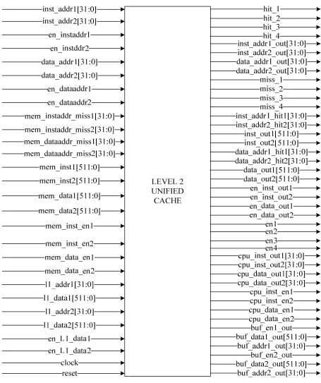
4.5.3 Level 2 Unified CACHE Design Specifications
Total number of sets in level 2 unified cache = 8
Total size of level 2 unified cache = 1 F
Set size in the level 2 unified cache = 6 6 +
6 2 6 +
=
F = 128 F
Size of each block in the level 2 unified cache = 21 + 2 + 512 ∗ 16 = 8245 rstq
Total number of lines in each set = 6 + + +
6 + 6m + +=
∗∗
≈ 127
Total offset bits = |zxqTt n|}T = |z16 = 4
Total index bits = |ztxtn| z}~rTp x |szTq sz Tngℎ qTt = |z127 ≈ 7
Total number of tag bits = txtn| noopTqq rstq − txtn| xqTt rstq + txtn| szoT rstq
= 32 − 4 + 7 = 21
A model Level 2 unified cache is shown in the Figure 4.8. Table VII in appendix I explains
30
FIGURE 4.8: Level 2 Unified Cache
4.6Main Memory
Miss address request sent by the cache is split into row and column addresses to access the
31
by the TLB’s. A model of the main memory is shown in the Figure 4.9. Table VIII in Appendix I
explains functionality of each of the input and output pins in the model main memory.
32
4.7Conclusion
The modules present in the two level cache model have been fully tested on Modelsim to verify
the complete functionality. Synthesizable working model of the two level cache is obtained by
using Leonardo Spectrum. The two level cache model is used as a test-bed for running power
analysis. The proposed power reduction techniques, adaptive phase tag cache and GALEOR will
33
Chapter 5
Proposed Power Reduction Techniques
Future generation processors employ long addresses to access data in memory resulting
in an increase in the tag field sizes. Increasing tag sizes result in an increase in the number of
comparisons, thereby increasing the dynamic power dissipation. Static leakage power is also
becoming a major concern in design of low power devices. The proposed techniques reduce both
the dynamic power dissipation caused by accessing the tag fields and the leakage current flowing
through the unused parts of the circuit.
5.1Adaptive Phase Tag Technique
Phase tag cache splits the address tag and tag matching into two phases. During the phase I, first
half of the cache tag is compared with the first half of incoming address tag. Phase II compares
second half of the cache tag with the second half of the incoming address tag. Width of the tags
remain unchanged throughout the execution of the program. Adaptive phase tag cache splits the
tag arrays & tag matching into two phases by varying the width of the tags during program
execution. Execution time of an application is divided into windows which samples a typical
instruction mix. During the phase I, first half of the incoming tag address is matched against the
first half of the cache tag array. When there is a tag match during phase I comparison, the second
phase tag matching is triggered. During a tag mismatch in the phase I comparison, the second
phase of tag matching is disabled. Disabling the comparisons during the phase II reduces the
switching power dissipation. During the phase II, second half of the cache tag array is matched
against the second half of the incoming address tag. When a tag match occurs in phase II,
requested data is sent to the CPU. Hit ratio is used as a performance metric to monitor cache
performance. Hit ratio is defined as
34
The Table 1 below shows allocation of tag bits for a model instruction cache having 23 bit wide
tag address.
Hit Ratio (HR) Width of Tag1 Width of Tag2
0.1 21 2
0.2 18 5
0.3 16 7
0.4 14 9
0.5 12 11
0.6 9 14
0.7 7 16
0.8 5 18
[image:48.612.144.472.394.647.2]0.9 2 21
TABLE 5.1: Allocation of Tag bits based on the Hit Ratio
Increase in the hit ratio results in reducing width of the first part of tag thereby reducing the
dynamic power dissipation. Reduced width in the first part of tag leads to large number of
accesses to high level caches increasing the delay overhead.
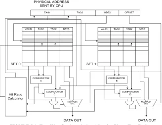
FIGURE 5.1: Two Way Set Associative Adaptive Phase Tag Cache
Model of a 2 way set associative adaptive phase tag cache is shown in the Figure 5.1. Index field
35
found the comparators A and B are used to compare the first half of the physical address with the
first half of the set associative cache tag address. During the second phase of tag matching,
Tri-state comparators are used to reduce switching activity. Tri-Tri-state comparators are obtained by
adding tri-state buffers to the inputs of a bi-state comparator. When the enable is low, a high
impedance state results at the output. When the enable is high, tri-state buffers pass the input data
to output. During a TAG1 hit, the set of tri-state comparators C and D are enabled to compare the
TAG2 of the physical address with the TAG2 of the set associative cache tag address. During a
valid cache hit, multiplexers are used to select the instruction and data requested by CPU based
on the offset value. Hit ratio calculator decides the widths of tags during phase I and phase II
based on the number of hits during phase I match. Increased cache tag sizes, result in an increase
in the number of tri-state buffers and also increases complexity of the hit ratio calculator logic,
thereby increasing the area overhead. Resizing cache tags introduces performance overhead due
to the increase in the number of phase II comparisons.
5.2GALEOR Technique:
Sub-threshold leakage contributes maximum for static power dissipation. Consider the NAND
gate shown in the Figure 5.2 with the source, gate and drain regions of each transistor
representing different nodes.
36
Sub-threshold leakage currents flowing through a two input NAND gate for different input
combinations are explained below.
i) A = 0 , B = 0 : When both the inputs are low, the PMOS transistors MP1 and MP2 are
turned ON while the NMOS transistors MN1 and MN2 are turned OFF. Reduced
sub-threshold leakage currents flow through the NMOS transistors MN1 & MN2 due to
the stack effect.
ii) A = 0 , B = 1 : The PMOS transistor MP1 and the NMOS transistor MN2 are turned
ON while the PMOS transistor MP2 and the NMOS transistor MN1 are turned OFF.
Sub-threshold leakage currents flowing through the OFF transistors MP2 & MN1
remain unaffected.
iii) A = 1 , B = 0 : PMOS transistor MP2 and NMOS transistor MN1 is turned ON while
the PMOS transistor MP1 and the NMOS transistor MN2 are turned OFF.
Sub-threshold leakage currents flowing through the OFF transistors MP1 & MN2 remain
unaffected.
iv) A = 1 , B = 1 : When both the inputs are high, the PMOS transistors MP1 and MP2
are turned OFF while the NMOS transistors are turned ON. Sub-threshold leakage
current flows through the PMOS transistors MP1 and MP2.
Leakage currents flowing through a two input NAND gate are summarized in the Table 5.2.
A B MP1 MP2 MN1 MN2
0 0 ON ON ISUB : t → w ISUB : w → x
0 1 ON ISUB : q → t ISUB : t → w ON
1 0 ISUB : p → t ON ON ISUB : w → x
1 1 ISUB : p → t ISUB : q → t ON ON
37
When both the inputs are low, natural stack effect is introduced thereby reducing the leakage
current flowing through the circuit. Rest of the input combinations does not introduce a natural
stack effect to reduce the leakage current. To reduce the leakage current flowing through the
circuit, forced stack effect needs to be introduced. The proposed technique, GALEOR,
introduces two additional transistors in the circuit to introduce a force stack structure in the
circuit independent of the input combination. Force stack structure added reduces the leakage
current by increasing the resistance of the leakage path.
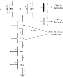
GALEOR technique implemented on a two input NAND gate is shown in the Figure 5.3.
A B
A
B
GLT1
GLT2
OUT
Gated Leakage Transistors
High Vth
Transistor
Low Vth
Transistor Vdd
MP1 MP2
MN1
MN2
p q
n s
t
z
r u
v w
[image:51.612.165.433.324.658.2]x
38
Additional gated leakage NMOS transistor GLT1 and a PMOS transistor GLT2 are introduced
between the output and pull-up circuitry and the output and pull-down circuitry. Sub-threshold
leakage currents flowing through a two input gated leakage transistor NAND gate for different
input combinations are explained below.
i) A = 0 , B = 0 : When both the inputs are low, the PMOS transistors MP1 and MP2 are
turned ON while the NMOS transistors MN1 and MN2 are turned OFF. Intermediate
node t is charged to supply voltage while the intermediate node r remains at the
supply voltage. Gated leakage NMOS transistor GLT1 turns ON while the gated
leakage PMOS transistor GLT2 is turned OFF since the gate voltage on the transistors
is less than the threshold voltage. Gated leakage transistor GLT2 introduces a forced
stack structure with the NMOS transistor stack further reducing the leakage current
flow.
ii) A = 0 , B = 1 : The PMOS transistor MP1 and the NMOS transistor MN2 are turned
ON while the PMOS transistor MP2 and the NMOS transistor MN1 are turned OFF.
Intermediate node t is charged to supply voltage while the intermediate node r
remains at the supply voltage. Gated leakage NMOS transistor turns ON while the
gated leakage PMOS transistor is turned OFF. Gated leakage PMOS transistor GLT2
forces a stack effect with the OFF transistor MN1 thereby reducing the leakage
current flow.
iii) A = 1 , B = 0 : The PMOS transistor MP2 and the NMOS transistor MN1 are turned
ON while the PMOS transistor MP1 and the NMOS transistor MN2 are turned OFF.
Intermediate node t is charged to supply voltage while the intermediate node r still
![FIGURE 1.1: 2002 Power Projections by ITRS [1]](https://thumb-us.123doks.com/thumbv2/123dok_us/60640.5655/15.612.119.498.431.696/figure-power-projections-itrs.webp)
![FIGURE 3.2: Gated Supply Technique [17]](https://thumb-us.123doks.com/thumbv2/123dok_us/60640.5655/27.612.209.400.220.377/figure-gated-supply-technique.webp)
![FIGURE 3.5: Sleepy Keeper [20]](https://thumb-us.123doks.com/thumbv2/123dok_us/60640.5655/29.612.229.389.271.436/figure-sleepy-keeper.webp)