A STUDY OF HIGH BRIGHTNESS PLASMA
ION SOURCES
A thesis submitted for the degree
of Doctor of Philosophy of
the Australian National University
Orson Sutherland
except where due reference is made in the text.
A c k n o w le d g e m e n ts
The human understanding is no dry light, but receives an infusion from the will and affections; whence proceed sciences which may be called “sciences as one would.” For what a man had rather were true he more readily believes. Therefore he rejects difficult things from impatience of research; sober things, because they narrow hope; the deeper things of nature, from superstition; the light of experience, from arrogance and pride, lest his mind should seem to be occupied with things mean and transitory; things not commonly believed, out of deference to the opinion of the vulgar. Numberless, in short, are the ways, and sometimes imperceptible, in which the affections color and infect the understanding.
Francis Bacon
1 think it is quite fitting, as 1 write this small note of appreciation, that 1 should be listening to J. S. Bach’s Toccatas and Fugues: for me, they express imperious majesty, sobriety, rational thought but always an ever curious, arabesque creativity and stirring beauty. It is also a reminder of a time when all human enterprises of high art were passed on through the generations from the master to the apprentice. In my mind there is no doubt, for all the help that I have received from others, that my deepest thanks, with respect to this work, go to my supervisor R. W. Boswell. I flatter myself to believe that Rod may have made of me a Baconian. Upon reflection, this is all I ever really wanted from my time as a doctoral student. That I have produced this book and perhaps contributed something to science is a happy consequence of a much more meaningful and rich experience and one that has marked me both as a scientist and as a person. The clarity of thought that I have developed in my training under Rod’s supervision is probably now my most prized possession.
The logic now in use serves rather to fix and give stability to the errors which have their foundation in commonly received notions than to help the search after truth. So it does more harm than good.
I also reserve many thanks for Christine Charles who has been most generous with her time in helping troubleshoot experiments and discussing results. I have always been awe-struck by her organisation and I am constantly reminded not to forget the small things.
I would also like to thank Montague Giles for developing the ion cyclotron theory and Andrian Ankiewicz for his invaluable help with the Langmuir-Blodgett gener alisations.
No tribute page in our laboratory would be integral or indeed just without the mention of Peter Alexander, our tireless technician. I think that we are blessed to have someone so skilled, so humble and so committed to the projects in the lab as our Peter. It will be a sad day when the time comes to fill his shoes but surely it is fair that even the most committed man may dream of an enjoyable retirement. I often wonder if among the ” youth of today” we might find someone that will re motely resemble what we have in Peter... There is something about him of the old world decency and commitment that I don’t detect among my peers.
In the same league is Dennis Gibson, from the Electronics Unit, who was in strumental in keeping WOMBAT’s RF system running. He was always available for advice both in the design and construction of electronic circuits but also in trouble shooting probes. The younger fellas in the EU are going to have some trouble fol lowing in Den’s foot steps when he finally decides he has had enough... nonetheless they are a great bunch of guys and I would like to acknowledge, in particular, David Anderson and Michael Birdsall.
Julie Dalco has gotten me out of many tight spots with her no nonsense ap proach to computer administration. But on this front, I owe a particular debt to Fenton Glass, who despite of (or is that because of ?) his major geekiness, has also become a good friend, one that I can always trust for a good laugh.
I’d like to thank all of my friends at the lab: Albert Meige, for reminding me to have fun; Devin Ramdutt, for reminding me to enjoy nature; Ane Aanesland, for reminding me that Latex syntax is important (and a special note of thanks for proof reading my thesis); Vicki Au, for reminding me th at dressing well gets noticed; Peter Linardakis, for reminding me to stay in touch with old friends; Fernando Gesto, for reminding me to appreciate simple human emotions; Nicholas Plihon, for reminding me not to take things quite so seriously; Michael Irzyk, for reminding me to appre ciate the finer things in life; John Keller, for reminding me to back myself; Helen Smith, for opening up the wonderful world of the Antarctic to me; Clive Michael, for reminding me to windsurf; Tristram Alexander, for reminding me just to take it easy; Hyun Jin Yoon, for reminding me to be patient.
vii
PhD in the family. Subsequent research has uncovered that this is not at all the case with a number of relatives (especially females) having Doctorate’s and in particular a noted historian. Nonetheless it is vindication for my parents and I hope an inspira tion to my siblings. This thesis is certainly something that they should feel a part of.
For me, writing this thesis was an singularly egocentric experience and I recog nise the hypocrisy of my comportment, simultaneously expecting understanding from those around me whilst putting on a steely air of control. I had no right to brood. However, I will say in my defence and all those that have and will suffer this fate, those who haven’t written a PhD thesis (or who didn’t find it a chal lenging experience) just can’t understand; so perhaps we ought not expect them to. Nonetheless, my Jane tried her darndest and stuck by me when she had every reason to leave.
As a final note and a bit of a tribute to Jane’s wit, I would like to share with you a Haiku that she wrote as a bit of a joke after reading the introduction to this thesis. She wrote several, but the one that I have presented here I personally think is brilliant. Those of you who know Jane will recognise her sense of humour. I hope that you will join me in agreeing that this is a most excellent work. It is pertinent, ingeniously humorous but simultaneously melancholic. A post-modern deconstruction of industrial man, forlorn amongst his machines.
Ions of argon
In a vacuum, through a mask March single file
A b s tr a c t
This thesis is concerned with the extraction of high brightness focused ion beams (FIBs) from radio frequency (RF) plasmas and presents both an experimental study of heating mechanisms in a helicon plasma ion source and a new perspective on the theory of extraction optics. Four prototype ion sources suitable for use with FEI Co. FIB columns are presented.
A new approach for the design of extraction optics which considers a more rigourous treatment of the plasma sheath, plasma/beam interface and beam distributions is presented. The theory treats the beam as an angular section of a complete classical diode as first considered by Langmuir and Blodgett but generalises the solutions to take into account the non-zero potential present in the plasma sheath. It also takes into account the convexity of the beam distribution solutions and proposes that to minimise emittance growth the electric field at the exit of the extractor must be zero requiring at least two stages comprising a total of 5 electrodes. The precise electrode geometries are then found by solving Laplace’s equation in two dimensions in the charge free region.
This theory makes the assumption of cold plasma ions which can lead to a signif icant departure from experimental reality. It is also known from thermodynamic considerations that the inherent brightness of an ion source is limited by the tem perature of the extracted species. Therefore some effort was made in this work to develop a high density, cold ion, plasma source. In particular, a source capable of densities up to 1014 cm-3 at the point of extraction is presented and both parallel and perpendicular heating mechanisms are investigated in some detail. In addition, it is shown how the parallel ion energy distribution can be controlled by “balancing” the RF antenna to minimise chromatic aberrations. Further improvements in ion energy spread are shown to be gained by the use of smaller extraction apertures and magnetic confinement of the source plasma. Finally, with the optimal mix of these parameters, the measured ion energy spread is shown to be with-in the 3 eV resolution of the measurement technique (as measured by Noel Smith of FEI Co.), and may, with subsequent measurements due for late 2004/ early 2005 be shown to be significantly less than this.
Un-der certain operating conditions ion cyclotron and ion acoustic wave activity was observed. Generation of the ion cyclotron wave is explained by a filamentation type instability (developed by Montague Giles) whilst the ion acoustic waves are believed to be driven by strong pressure gradients at the edge of the plasma column. It is shown that these waves exist for a relatively narrow range of parameters and can be avoided whilst still obtaining high densities.
Contents
A cknow ledgem ents v
S u m m ary of T hesis ix
1 In tro d u c tio n 1
1.1 N ano-Fabrication... 1
1.2 F I B s ... 6
1.3 Quantifying F I B s ... 8
1.3.1 A b e rra tio n s... 9
Spherical A berrations... 10
Chromatic A berrations... 11
1.3.2 E m itta n c e ... 13
1.3.3 Beam B rig h tn e ss... 14
Thermodynamic L i m i t ... 15
1.4 Ion Source T echnology... 17
1.4.1 Liquid Metal Ion Sources... 17
1.4.2 Duoplasmatrons... 20
1.4.3 Multicusp Plasma S o u rc e s... 22
1.4.4 Penning Sources... 24
1.4.5 RF Ion S o u rc e s... 25
1.5 Towards a High Brightness Plasma F I B ... 27
1.5.1 Electrode D e s ig n ... 31
Empirical Studies On High Intensity B e a m s ... 32
The Pierce G u n ... 32
Extending Pierce’s M ethod... 35
Generalising Langmuir-Blodgett’s L aw s... 35
Blocking Electrodes... 37
Engineering the Electric F i e l d ... 38
1.5.2 High Density Cold Ion Plasma Source Design ... 39
Helicon Plasm as... 39
Parallel Ion Energy D istribution... 41
2 E le c tro d e D esign for th e E x tra c tio n of V ery H igh B rig h tn ess Ion
B eam s 45
2.1 Statement of Problem ... 46
2.2 Beam D istributions... 49
2.2.1 The Basic Solution to Poisson’s E q u atio n ... 51
Spherical Symmetry ... 51
Cylindrical Symmetry ... 53
2.2.2 Non-Zero Initial G r a d ie n t ... 53
Spherical Symmetry ... 55
Cylindrical Symmetry ... 56
The Plasma S h e a th ... 56
Sheath Potential at the M e n isc u s... 57
Potential Gradient at the M e n isc u s... 59
D iscussion... 59
2.2.3 Solving Poisson’s Law B ack w ard s... 61
2.2.4 Presence of E lectro n s... 62
2.2.5 Non-Zero Initial V elocity... 63
2.3 Laplace’s E q u a tio n ... 64
2.3.1 Strip B e a m ... 65
2.3.2 Wedge Beam ... 66
2.3.3 Cylindrical B e a m ... 67
2.3.4 Conical B e a m ... 69
2.4 Method for the Design of Electrodes ... 70
2.4.1 Introduction... 70
2.4.2 The Extraction G a p s ... 70
Stage 1 ... 70
Stage 2 ... 71
The problem ... 71
2.4.3 Blocking Electrodes... 72
2.4.4 Beam N e u tra lis a tio n ... 72
2.5 An Example: A Diverging Wedge Beam ... 73
Extraction Gap Stage 1 73 Extraction Gap Stage 2 74
Blocking Gap Stage 1 ... 76
Blocking Gap Stage 2 ... 76
2.5.1 Closing rem a rk s... 76
S im u latio n s... 78
Plasma Density R a n g e ... 82
3 D iag n o stics 85 3.1 Langmuir P r o b e s ... 85
3.2 Ion Source D iag n o stics... 90
3.2.1 Density M easu rem en ts... 90
3.2.2 Beam M easu rem en ts... 92
C o n te n t s x iii
Angular Divergence... 92
Beam D istributions... 93
Sim ulation... 96
3.3 WOMBAT D iagnostics... 99
3.3.1 Langmuir Probes in W O M B A T ... 99
The Study of Basic Plasma P aram eters... 100
Spectral M easurem ents... 101
3.3.2 Microwave Interferometer ... 101
3.3.3 Retarding Field Energy A n a ly s e r... 102
4 D e v e lo p m e n t o f a C o m p a c t H ig h D e n sity P la sm a Ion S ou rce 107 4.1 The Experimental C oncept... 109
Vacuum System and Gas F e e d ... 109
RF System ... 112
Extraction S y s t e m ... 113
Diagnostic C h a m b e r ... 115
4.2 The P ro to ty p e s ... 115
4.2.1 Prototype 1 ... 115
General Description... 115
Ray-Tracing S im ulations... 117
Plasma Density Measurements... 118
The Effect of Power, Magnetic Field and Antenna Position . 119 4.2.2 Prototype 2 ... 122
4.2.3 Prototype 3 ... 124
4.2.4 Summary of Prototypes ... 126
5 P e r p e n d icu la r Ion H e a tin g 127 5.1 A Brief Introduction to Electromagnetic Waves in Cold Plasmas . . 127
Circular Polarisation and Resonance ... 130
5.2 Wave Particle In tera ctio n s... 132
5.2.1 Ion Landau D am ping... 132
5.2.2 Doppler Shifted Ion Cyclotron Resonance... 135
5.2.3 The Experimental S e t - U p ... 136
Vacuum V e s s e l...: ... 137
Magnetic Field S y s te m ... 138
RF System ... 140
Ar II Plasma Colum n... 143
5.2.4 Ion Cyclotron W a v e s... 146
Experimental Evidence of Ion Cyclotron W a v e s ... 146
Four Wave Resonant Interaction... 150
Ion Cyclotron Parameter S p a c e ... 154
D iscussion... 155
5.2.5 Ion Acoustic W aves... 158
Experimental O b serv atio n... 159
P re s s u re ... 163
P o w e r ... 163
Magnetic F i e l d ... 163
A Comparative Study ... 165
6 P a r a lle l Io n H e a tin g 167 6.1 Charge Exchange and Elastic Scattering Collisions... 167
6.2 Parallel Ion Energy S p re ad ... 176
6.2.1 Measuring Ion Energy Spread with a Mass Spectrometer . . 176
Energy Callibration of the Mass S p ectro m eter... 176
Initial Energy Spread R e s u l ts ... 179
6.2.2 Reducing Capacitive C oupling... 181
Balanced Antenna ... 181
200 gm Extraction A p e rtu re ... 182
Half Split Faraday Shield... 184
7 C o n c lu d in g R em a rk s 187 7.1 Extraction O p tic s ... 189
7.1.1 Generalising the Langmuir-Blodgett L a w s ... 189
7.1.2 Low Aberration Electrodes... 191
7.1.3 Electrons and the Extraction O p t i c ... 192
7.2 Plasma Source... 193
7.3 Ion Energy S p r e a d ... 194
CHAPTER 1
Introduction
1.1 Nano-Fabrication
It is an observable trend that the number of personal computers, mobile tele
phones and other portable micro-processor based technologies is increasing as the
functionality of such devices improves and their accompanying cost falls. The pro
cessing speed of micro-processors as well as the memory capacity of mass storage
devices is largely a function of the number of transistors that can be printed per
integrated circuit (IC) chip. According to the Semiconductor Industry Association
[86] road map, transistor density has been growing exponentially from 107 cm-2 in
1995 to 1.1 TO8 cm-2 in 2004 and will continue to do so in coming years attaining
5.6-108 cm-2 by 2010. Interestingly, the cost per chip has remained stable at around
USD 100 per unit and is expected to remain so. Although the transistor density
is increasing exponentially, the aggressive pace of contemporary systems designs
means that there is also a need to increase chip size from 250 mm2 in 1995 to 620
mm2 in 2010 to keep up with demands for increased processing power and memory
capacity at lower cost. This has two immediate implications: increased lithographic
exposure resolution (90 nm line width in 2004) to furnish the need for increased
transistor density, but also with the growing wafer size, increased exposure fields.
Increasing the wafer size is essential to maintaining throughput and hence keeping
to chip manufacturers as they are driven to increase wafer size from 300 mm in 2004
to 400 mm by 2007.
In the manufacture of ICs the enabling technology has been optical lithography
which, due to enhancements in stepper and lens technology, has seen it push the
need for next generation lithography (NGL) machines further and further into the
future. The technology that experts claimed was defunct a decade ago is still sup
plying the micro-electronics industry with ICs. However, despite it being generally
accepted that optical lithography is the technology of choice down to 200 nm, the
current push by chip manufacturers from 90 nm down to 65 nm feature size and
beyond will require a sustained technology evolution for which many of the technical
challenges have no contemporary solutions. According to Gross [45] in 1997, photo
lithographers seemed unanimous in thinking that the only and final step forward
for optical lithography then seemed to be to push the wavelength barrier one last
time into the deep UV (193 nm) to reach 150 nm resolution. Today, many IC fabs
have already implemented 193 nm DUVL machines for resolutions of 120 nm and
below. However, the optical adjustments required to work in DUV make this form
of optical lithography progressively more expensive. As a simple example, exposures
at wavelengths much below 157 nm have to be done under vacuum which drives up
the cost of the machine and slows throughput. Moreover, much below 126 nm, the
physical properties of all optical components including the mask and even air act
as reflectors opening the way for the new field of extreme UV lithography (EUVL)
and a complete redesign of much of the existing lithography technology. Typically
EUV research centres around wavelengths close to 13 nm and has been shown to
successfully produce features of less than 70 nm in dimension [89]. However, for
use in mass production there is quite some way to go for this technology which still
must overcome a number of technical issues with mask fabrication ([53], [92], [82],
1.1 N a n o -F a b r ic a tio n 3
At even more extreme wavelengths is the field known as proximity x-ray lithogra
phy (PXL). Again, this technology has proven its ability to mill features as small
as 35 nm but is hampered by current mask technology which has trouble keeping
pace, especially in the context of mass production [1]. The trade-off in increased
resolution is closer proximity between the mask and the wafer which can be as little
as 5fim. At this distance mask rigidness, thermal expansion effects and particulate
contamination become real issues for mask maintenance and lifetime. Moreover,
PXL is a unity demagnification system which puts tight constraints on the contri
bution of mask alignment, beam uniformity and mask feature resolution to the edge
to edge overlay budget [45]. Mizusawa et al. [93] have presented a production ready
exposure tool for PXL but as yet there have not been any real solutions to mask
and resist technology. In addition, the 1 nm range x-rays are generally produced
using a synchrotron so that the manufacturing floor would need to be signihcantly
altered to accommodate between 10 and 20 exposure stations for every x-ray source
[89],
Many of the technical difficulties associated with diffraction through the mask are
avoided by using electrons or ions as the exposure medium. At 100 keV, electrons
have a DeBroglie wave length of 4 • 10~3 nm whilst Hydrogen ions have a wave
length on the order of 5 • 10-5 nm. For ions, diffraction limits are well below 5 nm
even with a numerical aperture (NA) as small as 10-5 rad. That electrons and ions
are able to expose resist has been known for over 2 decades [89, 39], but they are
particularly effective since they provide very even dose and minimal scatter in the
resist [106]. Standard resists can be used without modification and in the case of
ions the exposure can be extremely rapid, about 0.5 s, with exposure fields up to
100 mm2 [46]. On the other hand, electron beam exposure requires much greater
currents than ion beam exposure and so is limited by space charge effects in the
only expose fields on the order of 1 mm2 due to a relatively large NA of 10-3 rad.
Nonetheless, electron projection lithography (EPL) has been in use for some time
in areas where throughput is less critical such as in the fabrication of lithography
masks [89, 120, 39].
Up until recently, ion projection lithography (IPL) was shaping up to be a leading
contender as an NGL device for high throughput fabrication of ICs. Most of the
underlying technology such as stepper, mask and resist already existed and did not
need to be modified. Loeschner et al. [84] had shown that IPL could effectively
write 100 nm lines over an area of 12.5 x 12.5 mm2 whilst Kaesmaier et al. [65] had
demonstrated, using analytical modelling, that these sub-fields could be “stitched”
together to expose an entire wafer using a new stitching technology. The main
constraint in these systems was the ion source which typically produced ions with
anywhere between a 2 and 15 eV energy spread. In early experiments Duoplas-
matrons were used as a source of ions but these systems had an energy spread of
between 10 and 15 eV [46]. This severely limited the resolution of the IPL device
as a whole through blurring produced by chromatic aberrations in the optical col
umn. In more recent tests a multicusp ion source developed at Lawrence Berkeley
National Laboratory (LBNL) by Leung et al. was employed [80]. With a magnetic
filter integrated into the system ion energy spreads as low as 1 - 2 eV were mea
sured [80, 76]. It was this source that formed the basis of the most recent results at
the Fraunhofer Institut in Berlin [77] and IMS in Vienna [65]. However, the short
life-time of the multicusp source especially for the filament device will no doubt
exclude it as a viable option for production ready machines [76]. Some work is still
being undertaken on an immersed, porcelain coated RF antenna design which has
shown more promise for life-time considerations but which has a higher ion energy
spread [77]. Though it is claimed that the filament driven multicusp source has an
1.1 N a n o - F a b r ic a t io n 5
Scipioni et al. reported that this same source produced only an intermediate bright
ness of 1650 A.cm-2.sr_1. In any case, modelling performed at Siemens-Munich AG
[46] has shown that assuming a virtual source size of 10 fim and an energy spread of
1 eV (unfortunately an equivalent brightness was not quoted) that 100 nm features
with a pattern density of 50% can be printed over a 22x22 mm2 area at a rate
greater than 75 wafers per minute (WPM). Kaesmaier et al. ([65]) subsequently
showed results from modelling that produced sub-50 nm resolution using stitching
techniques.
It would seem, therefore, that a leading candidate for NGL is ion projection lithog
raphy, as it has a demonstrated production capability and has clear and apparently
solvable technical challenges for evolution over several generations of shrinkage. One
of the main challenges facing IPL is treated in some detail in this thesis, notably
the design of a high current density plasma ion source with low ion energy spread.
However, perhaps the greatest obstacle to IPL, according to the 2003 SEMATCH
road map, will be the incumbent technology of optical lithography which it appears,
despite a number of technical challenges in all aspects of the production process,
will be able to continue on to 2009 and to feature sizes as small as 15 nm, by driving
into the EUV. It is still unclear whether the process cost will become prohibitively
expensive as more sophisticated methods are required to allow for ever decreasing
wavelength, but SEMATECH ([107]) is confident that the next decade will almost
certainly be dominated by optical lithography. According to Loeschner, IPL is now
almost defunct but novel multi-beam lithography techniques are being developed as
an alternative to optical processes should SEMATECH’s prediction be wrong (L.
Scipioni, FEI Co., private communication). These multi-beam systems still have
at their core variable species, high current density, low ion energy spread plasma
sources so that the research presented in this thesis is of some importance to their
1.2 FIBs
Another area of direct relevance to the semiconductor industry both in terms of
the mass production lithography process and the related field of metrology is the
production of focused ion beams or FIBs. These become relevant in both mask
modification and correction, surface analysis, failure analysis, defect characterisa
tion and process control functions.
Masks are commonly made using a plasma etch technique but often have imper
fections, typically an unintended opaque spot in a clear field or vice-versa, which
left untreated would result in errors in the IC. With the increasing size of dies the
probability of imperfections augments as the inverse of the area:
Y = ----
---l + D.A
where D is the density of random defects and A is the die area on wafer. For multi
level structures to obtain a final yield of as little as 50%, the yield of any single
layer must be greater than 88% [39]. Imperfections are virtually unavoidable and
can have cost and performance ramifications further along the production process
if not treated early. FIBs are ideal for mask correction because they can be used
to sputter away and deposit material at the location of the imperfection with a
nano-metric scale beam of ions. It is tempting to ask whether FIBs could be used
to direct-write the entire mask as they can reproduce features on the order of 10
nm, but alas the process is far too slow for high-throughput production and hence
is not cost effective.
Because FIBs have such high precision milling capabilities, they are also finding use
in tunnelling electron microscopy (TEM) sample preparation [61], [60], [96], [108],
[128], [129]. TEM is a method for analysing the chemical composition and thickness
of layers on the surface of a material. A thin slice, usually between 50 - 100 nm
1.2 F I B s 7
FIB and then eutectically soldered to leads for transfer to a TEM workstation where
its various stratifications can be analysed, much like geological analysis of soil. A
similar technique can be used to troubleshoot components in ICs. Wang et al. have
developed a electron holoscopy technique for the 2 dimensional characterisation of
p-n junctions [126]. The technique is based on TEM where a wedge shape sample
is cut from the circuit using a FIB in a similar fashion to standard TEM sample
preparation techniques.
Another important measurement in the design, development and fabrication of ICs
is the size of critical features such as linewidth, wall profiles and edge-to-edge over
lay. Undercut profiles and pattern shift effects originating from the etching and
mask imaging processes respectively can impact on design tolerances and mask per
formance during the lithography process and must be controlled precisely. The slope
of the interface between the clear and opaque regions of a mask, usually called the
mask walls, define the undercut profile and is directly related to the transmittance
of the mask. Pattern shift on the other hand, which is defined as:
AS = Wc - W m (1.2)
where Wc is the pattern width of the copy and is the pattern width of the
master mask, determine the final size of the reproduced circuit layer. Obviously, in
contemporary multi-layer designs edge-to-edge overlay is critical and hence control
of the pattern shift is fundamental.
Design tolerances, development cycle time, manufacturing yield and circuit perfor
mance depend on the accurate measurement and control of these type of feature
sizes. In order to achieve adequate circuit performance, these features must be
controlled to with-in 10% of the total feature size. For 100 nm linewidths this
means an error of 10 nm or less, but ideally should far less than this. Wagner et
al. pointed out that “gross differences in measurement accuracy” can exist between
their paper they demonstrated that FIBs can be used for accurate critical resist
dimension metrology. Orloff et al. go further and point out that FIB imaging (or
scanning ion microscopy, SIM) is often preferred over higher resolution scanning
electron microscopy (SEM) techniques because there are different contrast mecha
nisms available with either secondary electron or secondary ion detection [95].
1.3 Quantifying FIBs
Focused ion beams constitute any group of largely mono-energetic ions with di
rected velocity, extracted, focused and accelerated from a source of ions, typically
by a series of electrodes that create a shaped static electric field. The term largely
mono-energetic is used because in all practical systems, the source of ions is not
cold and has some distribution of temperatures which is imparted on the individual
beamlets both parallel and perpendicularly to the directed motion. Typically, the
ion temperature in the source is several orders of magnitude less than the energy
gained from the extraction held and so in many applications can be ignored entirely.
However, for the work presented in this thesis ion temperature is a significant pa
rameter.
Beam geometry plays an important role in the development of the theory in this
work. In a macroscopic sense FIBs are differentiated by the geometry of the aperture
through which they are extracted. FIBs extracted through rectangular apertures
are referred to as strip or wedge beams whereas beams extracted through circular
apertures are denominated cylindrical or conical depending on whether they are
convergent, divergent or parallel.
A beam is dehned as laminar if after passing through an ideal convergent lens all
the trajectories converge on one point. A consequence of this definition is that
1.3 Q u a n tify in g F IB s 9
extent to which a beam is laminar is strongly tied in with the quality of the beam
which will be discussed in the following sections on aberrations and beam brightness.
1.3.1 Aberrations
The same type of lens errors which are found in light optics are found in charged
particle beam lenses. These errors are referred to as aberrations and occur when
rays leaving a point on the object converge on different image points.
In charged particle optics, aberrations arise from various sources. If it is assumed
that the charged particles emanating from the source are strictly mono-energetic
and that the extraction optics are perfectly aligned, then any deviation from the
ideal image is referred to as geometric aberration. These are also commonly called
third-order aberrations as they arise when the beam diverges from the paraxial
ray approximation. In the basic linear optical theory the half angle of arrival (or
departure) of a ray, 9, is assumed to be smaller than 7r/20 so that the error in
the approximation sin(9) ^ 9 is less than 0.1%. In many ion sources (especially
plasma sources), relatively large extraction apertures are required hence sin($) can
no longer be closely approximated by the first order term in the series expansion:
n3 n5
sin($) ~ 9--- 4— - — ... (1-3)
3! 5! v ;
In light optics 9 often has large values as many of the aberrations can quite easily be compensated for, however, in ion optics, due to complications in the physics, 9
can not be increased too much. Nonetheless, even if an angle as extreme as 9 = 7t/4 is considered, the error incurred by making the third-order approximation is only
0.5%. Therefore, deviations from the paraxial approximation can be analytically
investigated with quite a good degree of accuracy by considering only the first two
terms of the series expansion 1.3. This is called third-order theory and will not be
that it describes: distortion, anisotropic distortion, curvature of field, astigmatism,
anisotropic astigmatism, coma, anisotropic coma and aperture defect (otherwise
known as spherical aberration) [35]. It is this last aberration type that will be of
most interest to this work as it has the most dramatic impact on the final spot
size in FIB systems. The other aberration types pertain more to the high-fidelity
reproduction of patterns as in projection lithography applications.
If it is now no longer assumed that the electrode apertures are perfectly concen
tric and parallel, then a deviation in the Gaussian image plane occurs, even in the
paraxial limit, due to aberrations of asymmetry.
To further complicate the picture, any axial energy spread in the plasma ions results
in a non-uniform extraction velocity leading to an error phenomenon called chro
matic aberration. Axial energy spread can result both from inherent ion heating
mechanisms in the plasma and fluctuations in the plasma potential. Thermal effects
can be caused by collisions and wave-particle interactions as discussed in chapters 5
and 6 whilst oscillations in the plasma potential result from capacitive coupling at
the RF driving frequency between the antenna and the plasma (again c.f. chapter
6). Oscillations in the plasma potential effect the velocity of the particles as they
transit the sheath and when this transit time is comparable to the ion plasma period
can result in a distribution of exit velocities (c.f. Parallel Ion Energy Distribution).
Spherical Aberrations
A lens exhibits spherical aberration when its focal lengths for paraxial and
marginal rays are different. Typically for a convergent lens, the latter are more
strongly focused so that there exists a continuity of focal points along the axis up
to the paraxial focal point as shown figure 1.1. A screen placed normal to the axis
at the paraxial focal point would show a bright central spot surrounded by a series
1.3 Q u a n tify in g F IB s 11
1. Marginal Rays 2. Paraxial Rays
3. Convergent Lense
4. Marginal Ray Focal Point
5. Paraxial Focal Point
6. Gaussian Image Plane
Figure 1.1: Ray tracing of convergent lens effected by spherical aberrations.
spherical aberrations are the only type to exist for a point on the axis. It is largely
due to the aperture size and is the same for all points on the object. The aberration
figure in the Gaussian plane is a circle of radius proportional to the cube of the
aperture radius [35].
T h e theory presented in C hapter 2 is aimed in large p a rt a t minimising spherical
aberrations in the ex tracto r where for zero ion te m p eratu re all particle trajectories
are laminar.
C hrom atic A berrations
Ju st as in light optics, where different wavelengths of light “see” different indexes
of refraction, ions of different velocities can be th o u g h t of as changing the refractive
index of the medium through which they travel, resulting in differential optical
behaviour. Thus slower ions (longer wavelengths) are focused more sharply th an
faster ions (shorter wavelengths) and th e image becomes m arred. All real ion sources
have some ion therm al energy d istribution producing variations in focus th a t reduce
beam brightness. The energy spread in a plasm a m ight be a small fraction of the
to preclude the focusing of nano-metric beam spots. If only chromatic aberrations
are considered the minimum spot size, d, for a beam with an axial energy spread of
AE is:
where C is the chromatic aberration coefficient of the focusing lens, a is the half
angle of the beam arriving at the hnal focal spot and E is the total beam energy.
This equation shows that the final spot size is proportional to the ratio of the axial
energy spread and the total energy of the beam. It also demonstrates that the
length of the focusing column is a practical constraint on the system as the final
spot size is directly proportional to the half angle of arrival.
Unlike light optics where chromatic aberrations can be almost completely removed,
ion optics can not be designed to do so. The defect is with the object, or ion source,
and even a well designed lens will be subject to chromatic aberrations if the ion
source is not sufficiently cold or oscillations in plasma potential can not be reduced
below a suitable threshold.
This effect is particularly important in low energy FIB applications where the beam
energy can be on the order of 100 eV. In this case, an axial energy spread of 10 eV,
not uncommon for both Duoplasmatron and liquid metal ion source (LMIS) systems
represents an unacceptably large portion of the total beam energy and results in
strong chromatic blur. The relatively low inherent thermal ion energy spread of RF
ion sources (< 1 eV) makes this technology particularly suitable for low energy FIB
applications.
At higher extraction energies (> 10 keV), chromatic blur is minimised and often
becomes less important than both geometric and spherical aberrations.
1.3 Q u a n tify in g F IB s 13
1.3.2 Emittance
Any force that acts over a length scale large compared with the inter-particle
spacing preserves the phase-space volume of the beam distribution [56]. In one di
mension, phase-space is a plot of velocity versus position in a given direction for all
the particles in a beam in a given plane. Non-linear field components and fringing
fields (third-order aberrations) of focusing lenses can stretch and distort the distri
bution. To designate the quality of a beam a figure of merit is commonly employed
based on the effective volume occupied by the distribution, called emittance. This
quantity describes the transverse motion of particles in a beam and in one dimen
sion of phase-space is defined as the area of the smallest ellipse to circumscribe all
the points in the distribution:
The beams most common in FIB applications have cylindrical symmetry and so
£x
As a simple example, figure 6.4 shows the phase-space representation of an ideal
diverging wedge beam and the same beam distorted by spherical and chromatic
aberrations. Transversally, an ideal wedge beam has infinite extent in the y direction
and hence all space charge forces cancel so that its emittance is determined solely
by the distribution of points in the x — vx plane. These points lie about a line and
the closer the beam particles are to this line the lower the emittance and hence the
more laminar the beam is.
The angle of the line is directly related to the angle of divergence of the envelope
where a positive slope represents a divergent beam and a negative slope a convergent
beam. Distributions lying around the horizontal axis are parallel beams.
Non-linear forces distort the distribution. A distribution that emanates from the
plasma with particles lying close to a line in phase-space will be distorted into an
and particle therm al effects will lead to a broadening of the d istribution away from
th e line. Thus, as no source of ions is ever ideally cold the phase-space distribution
can never be a perfect line.
Figure 1.2: Trace and phase space diagrams. Top: trace space diagram of diverging wedge beam through 3 electrodes. Bottom: phase space diagrams. Bottom left: ideal wedge beam. Bottom center: wedge beam with spherical aberrations. Bottom right: phase space broadening due to ion temperature.
1.3.3 Beam Brightness
A nother useful figure of m erit is beam brightness providing inform ation not
only on the beam quality b u t also its intensity. Brightness is directly related to the
quan tity of current th a t can be delivered to a focused spot and thus is the prim ary
Vx Vx Vx
[image:26.526.88.424.155.501.2]1.3 Q u a n tify in g F IB s 15
metric for FIB applications. In its basic form it is defined as the current density
per unit solid angle in the axial direction:
B = d l
dtt.dS (1.6)
As FIBs commonly have Cartesian symmetry in the transverse direction, brightness
can be expressed as a function of emittance:
ß = - r —
7C e x £y
If ex = ey then the beam is isotropic and brightness can be expressed in terms of
the average emittance e:
7r2 e 2
Importantly, this expression shows that brightness is directly proportional to beam
current and emittance, noting that if emittance is conserved, then beam brightness
is constant throughout the extraction and transport regions.
Thermodynamic Limit
Even with close to ideal lenses there is an ultimate limit to the brightness that
can be achieved with any given source which is dependent on ion temperature.
The thermodynamic limitations to brightness derive from the fact that the particles
emitted from the plasma have a Maxwellian energy distribution with a most proba
ble energy of kTi and an average energy of 2kTi, where k is the Boltzman constant
and Ti is the mean ion energy in eV. If it is assumed for simplicity that the ions
are accelerated in a parallel, uniform electrostatic field which adds only to parallel
energy, leaving the perpendicular energy unchanged, and that the parallel velocity
is much greater than the perpendicular velocity, then the half-angle of divergence
is given by:
e
^vii
The electric field accelerates the ions through a potential drop, V, so that the parallel
velocity can be written:
^ = ' / 2m v (1.10)
where e is the elementary charge and Mi is the ion mass. A similar reasoning can
be applied to obtain the perpendicular ion velocity by equating the most probable
energy to the kinetic energy:
n = ( i . i i )
Since brightness is defined in terms of solid angle, 6 must be converted to stera-
dians. This is done by noting that solid angle is the area defined by the surface
of intersection between a cone of half-angle 0 and the unit sphere, where the cone
apex is concentric with the centre of the sphere. A simple calculation yields the
solid angle, a, as a function of half-angle, 9:
a = 27r(l — cos(0)) (1.12)
Since # <C 1 equation 1.12 can be rewritten in terms of a Taylor series:
a ~ 27t^1 — ( l — —J J — k62 (1.13)
and the beam can be considered quasi-parallel. If, in addition, it is assumed that
the current density is uniform across the whole area of the extraction aperture, then
the current density can be assumed to be isotropic so that the brightness can be
rewritten:
d 3 3 JeV
a nO2 nTi
where j is the current density and T* is in eV. This equation was first derived by
Langmuir in 1937 and demonstrates that brightness increases as a function of current
density and extraction potential and decreases as the inverse of ion temperature. In
the thermodynamic limit, the denser and colder the plasma the brighter it is as an
1.4 Io n Sou rce T ech n o lo g y 17
reality lens aberrations play an important role in decreasing the effectiveness of FIB
systems. Ultimately, however, even without considering spherical and chromatic
aberrations it shows that FIB extraction is limited by irreversible emittance growth
caused by inherent thermal mechanisms in the plasma. In addition, it demonstrates
that the brightness of a plasma ion source is limited by practical constraints on
the maximum plasma density (effecting extractable current) and extraction voltage
that can be attained in real systems.
As an example, if ions are extracted at 10 kV from a plasma of density 1019 m~3 with
an ion temperature of 0.1 eV, then the thermodynamic limit on beam brightness is
approximately 104 A.cm-2.sr-1 . This is relatively low when compared with LMIS
systems which can provide beams with brightness two orders of magnitude higher
than this. It doesn’t seem unreasonable, however, to design a source with a density
of 1014 cm-3 and an extraction potential of 100 kV which would provide comparable
results. It should also be mentioned that there are numerous applications for inert
gas ion sources of intermediate brightness on the order of 103 - 104 A.cm_2.sr_1
which are well with-in the limits of the technology presented in chapter 4 (N. Smith,
FEI Co., private communication) . A typical application is surface analysis where
a relatively high current beam on the order of 100 nA with a micron resolution is
applied to a surface at intermediate (10 keV) and low (100 eV) energies.
Equation 1.14 underpins the primary emphasis of this work which is the develop
ment of low spherical aberration electrodes supplied by a cold ion plasma source.
1.4 Ion Source Technology
1.4.1
Liquid Metal Ion Sources
The semiconductor industry has had sub-micron milling capability for some
ions^ [116] and is used on almost all FIB systems employed in the semiconductor
industry [88]. Focused spots with diameters under 10 nm and current densities be
tween 1 and 10 A.cm-2 are now routinely obtained [95, 2]. The LMIS FIB system
has found extensive use across a wide range of applications in the manufacture of
ICs including design modification, failure analysis, defect characterisation and pro
cess control functions. However, they are unsuitable for low energy FIB applications
because they have a minimum axial energy spread of 5 eV [94].
The device works by field emitting ions from the tip of a sharp needle (usually tung
sten) over which a liquid metal such as gallium has spread by capillary effect. The
liquid metal is stored in a reservoir and, being usually solid at room temperature,
is heated to ease the flow over the tip. In the case of gallium, the metal is liquid at
room temperature in vacuum and the heating process is mostly to evaporate surface
contaminants and gallium oxide. An electrode in the form of an annulus, concentric
with the emitter and some distance below it applies an electric field to the tip where
it is concentrated and exerts a stress on the metal surface lifting it into a cone of
some 10 nm in diameter at its apex. The cone, referred to as the Taylor cone [119],
does not sharpen without limit because the field emission of ions at the tip is a
sufficient restoring force to maintain stability. Two explanations for this have been
proposed. The first reasons that the sharper the tip becomes the greater the field
that is concentrated there and as a result the higher the emission current. As the
emission current increases space charge builds up in front of the tip, blocking the
effect of the applied field. The alternative analysis provides that the hydrodynamic
properties of the liquid metal flow down the needle limits the available current and
as a result determines the I-V characteristics of the source. It has been found that
the radius of the needle tip and its surface roughness play an important role in
the current emission characteristic of the source, making the latter hypothesis more
1.4 Io n S o u rce T ech n o lo g y 19
generally accepted but by no means proven beyond reasonable doubt [88].
The metals used for LMIS can be of any composition as long as they wet the
1. Ceramic Plate 2. Tungsten Filament 3. Tungsten Needle 4. Annular Electrode 5. Liquid Metal Reservoir 6. Liquid Metal 2. —
7. Taylor Cone 3. —
6. —
3 —
-Figure 1.3: Conceptual diagram of a LMIS system with close-ups of the field emission tip.
needle, do not corrode the surface and have a low vapour pressure in the molten
state. Typically, metals with melting temperatures below 300°C are employed. Al
loy sources include: Au/Be/Si or Pd/A s/B and require a mass separator stage to
isolate a single ion species for implantation into the sample. It is also preferable
in FIB optics to have only a single ion species, and indeed a single ion isotope,
so that stray B fields (for example from a magnetic objective lens of a coincident
electron column) do not mass separate the beam and hence smear it at the sam
[image:31.526.166.382.141.457.2]trajectories through the final focusing lenses if a nearby magnetic lens or ion pump
magnet is not well enough screened. By far the most commonly used metal in
LMIS, especially in industry, is gallium (and in particular isotopically pure 69Ga)
since it is almost liquid at room temperature and yields long life-time sources. A
typical LMIS construction is shown in figure 1.3. A small tungsten needle is spot
welded to the apex of a tungsten filament formed into a loop and anchored in a
heat proof insulating base. The liquid metal is then held between the loop in the
filament and the shank of the needle by surface tension. For metals that are not liq
uid at room temperature a current is passed through the filament to heat the metal.
1.4.2 Duoplasmatrons
The Duoplasmatron has found wide use in a number of research and industrial
settings [56]. For example, in the early work on IPL it was the preferred source
of ions for resist exposure [112, 89, 46, 65, 84]. It was also commonly used in sec
ondary ion mass spectrometry (SIMS) [23]. Typically, the Duoplasmatron is used
for the production of relatively high current beams with peak currents up to sev
eral hundred milli-Amperes [111]. However, for high brightness applications, it is
limited by a relatively large axial energy spread of between 10 - 20 eV [111, 123].
Perhaps the Duoplasmatron’s biggest disadvantage is its short life time. Though,
Coath and Long [23] claim “long lifetime” to be among its chief advantages, Noel
Smith’s (of FEI Co.) experience with Duoplasmatrons working at both Cambridge
Mass Spectrometry (in the U.K.) and Physical Electronics (in the U.S.A.) was that
the best possible life time for these devices was 1000 hours for the cold cathode
model, though 250-500 hours was more typical. Life times well in excess of 1000
hours are required for efficient use “in-line” in a semiconductor fabrication process.
Even in less production critical environments, longer life-times are desirable. Often
1.4 Ion S o u rce T ech n o lo g y 21
perform even less well than this. The quoted lifetime for the Peabody Scientific hot
cathode Duoplasmatron was 150 hours. Hot cathodes are typically used for inert
gases and cold cathodes for oxygen.
The main cause of the Duoplasmatron’s short lifetime is sputtering of the cathode
by high energy ions of between 300-400 eV. The sputtering itself reduces the use
ful lifetime of the device by eroding the cathode, but the most common cause of
premature failure is sputter deposited material blocking the source aperture and
even in some cases the intermediate electrode aperture (N. Smith, FEI Co., private
communication).
Intermediate brightness’ have been reported for Duoplasmatron supplied ion beam
systems. The device used by Stengl et al. [112] in 1986 on their early IPL studies at
IMS produced a current density of 10 ^A.cm-2 on the target and, it was claimed, a
Figure 1.4: Conceptual diagram of a Duoplasmatron.
[image:33.526.114.416.381.628.2]later quoted a brightness of 1.7 • 103 A.cm-2.sr-1 with Ar+ ions at an extraction
energy of 15 keV from a Duoplasmatron optimised for FIB applications. However,
the large axial energy spread of these systems makes them unsuitable for low energy
(< 1 keV) and nanometric FIB applications.
The original Duoplasmatron was designed by von Ardenne [124] in 1963 and a
generic device is illustrated in figure 1.4. It works by thermionic emission of elec
trons from a tungsten filament ionising neutral gas atoms as they are accelerated
towards an anode. An intermediate electrode, called the focusing electrode stands
between the cathode and the anode (usually floating) and funnels the neutral gas
towards a narrow aperture where a plasma bubble is produced. This relatively
diffuse plasma supplies electrons to a second, much denser, magnetically confined
plasma produced between the intermediate and anode electrodes. This dual low
density/ high density plasma system is the origin of the device’s name.
Humphries [56] states that extraction voltages in the range of 50 kV can be applied
for moderate current applications, though Stengl et al. [112] applied between 60
and 90 kV in their work.
1.4.3 Multicusp Plasma Sources
The multicusp ion source, sometimes called the magnetic bucket source, is char
acterised by an array of permanent magnets that covers the walls of the plasma
chamber as shown in figure 1.5. In filament type multicusp sources, thermionic
electrons are emitted from a hot filament, typically constructed from tungsten, and
accelerated towards the chamber walls which act as an anode. Multipole fields of
a few kilo-Gauss localised near the wall reflect a large portion of the primary in
cident electrons, increasing their residence time in the source and thus promoting
ionisation and higher densities. The magnetic fields do not effect the emittance of
1.4 Ion S o u rce T ech n o lo g y 23
1. Filament
2. Multipole Magnets
3. Source Tube
4. Extraction Electrodes
Figure 1.5: Conceptual diagram of a Multicusp source
is field-free [56].
It has been shown by workers at LBNL that the addition of a magnetic filter just up
stream from the extraction aperture can significantly reduce the ion energy spread
of the beam ions improving brightness [80, 76, 81, 77]. Measurements using a 2 grid
retarding field energy analyser have shown energy distributions as low as 1 eV can
be achieved with the filter in place [77] as compared to 6 eV without it. Unfortu
nately, the filament, working by evaporation, has a limited operational life-time of
around 100 h and is thus unsuitable for use in IC production tools.
This problem can be solved by replacing the filament, anode/cathode structure with
an RF system. Because of the array of magnets on the chamber wall, the antenna
can not be wound around the outside of the source and instead must be immersed
coating but stochastic heating of ions in the antenna near field can not and leads to
increased ion energy spreads [76]. Lee et al. [76] reported that the LBNL magnetic
filter was not effective in reducing the ion energy spread in the extracted beam and
claimed RF induction fields were penetrating into the post filter region causing ion
energy spreads as high as 8 eV. More recently Leung [81] presented results showing
that the use of a magnetic filter reduced the ion energy spread from 10 eV to as low
as 2 eV.
1.4.4 Penning Sources
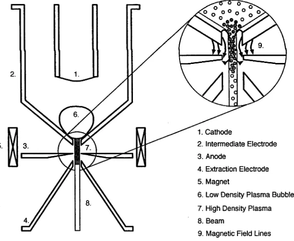
The Penning Ionisation Gauge (PIG) source has not commonly been used in IC
fabrication or research programs, though some recent interest has been shown in
this technology at the University of Maryland [48, 47]. At first glance it appears
to be an attractive option for IPL and FIB applications because it has a relatively
1. Cathode
2. Anode
3. Magnet
4. Extraction Electrodes
Figure 1.6: Conceptual diagram of a Penning ion source
high current density of several A.cm 2 and a reasonably low ion energy spread of
1.4 Ion S o u rce T ech n o lo g y 25
spreads as low as 0.6 eV for emission current densities of 1 A.cm-2 but report that
perpendicular ion energy increases with beam intensity (higher extraction voltages).
No mention was made of the overall source stability, though Humphries mentions
this as a chief disadvantage of these systems [56]. He singles out plasma instabilities
resulting from the crossed electric and magnetic fields as the cause of increased ion
temperature and large spatial and temporal variations in the plasma parameters
under various operating regimes.
Typically, PIGs are used for high current applications such as particle accelerators
[4, 62],
As with the Duoplasmatron, the PIG ion source is limited in practice by short life
time due to sputtering erosion of the cathode. Again, both hot and cold cathodes
are employed, where hot cathodes are typically used for inert gases and cold cath
odes are used for oxygen.
The device works by the emission of electrons from either a hot or cold cathode
which ionise neutral gas particles as they are accelerated towards the anode. The
discharge is struck in a small cavity formed between the anode and the cathode in
which an axial magnetic field and a radial electric field is applied as shown in figure
1.6. Electrons are trapped radially by the magnetic field and axially by the electric
field and as a result follow complex trajectories with-in the volume of the source
leading to longer residence times and hence ionisation.
1.4.5 RF Ion Sources
Given the apparent lack of RF ion sources in use by the semiconductor industry,
it is perhaps surprising that the first attempt to form a FIB was done using a system
adapted from a standard RF ion implanter dating back to 1973 [88]. It produced a
beam diameter of 3 and was used to expose Polymethylmethacrylate (PMMA)
processes were very slow, but the potential of the system was demonstrated. A
number of RF plasma ion sources have been developed by various research groups
over the years, but these sources are often multi-aperture devices for use in large
area processing of materials, neutral beam injectors for fusion and space propulsion.
Single aperture RF devices other than the multicusp type developed at LBNL are
more rare and certainly are not commonly used in the semiconductor industry. An
exception to this is a single aperture helicon ion source developed at the Korea
Advanced Institute of Science and Technology (KAIST) by Hwang et al. for use
in both a neutron spallation source and in accelerator driven transmutation tech
nology. This device produced a 200 mA beam at 50 kV with a divergence angle of
260 mrad [57]. No brightness measurements were presented.
Examples of multi-aperture ion sources are those described by Hayes et al. [51] and
Irzyk et al. [59], where the work of Irzyk et al. is of particular interest here because
it was based on a helicon reactor developed at the Australian National University
(ANU) and is similar in concept to the devices presented in this work. In his PhD
thesis, Irzyk showed that a helicon discharge was an efficient way to produce a high-
density, uniform plasma for ion extraction applications [58].
As will be shown later in this work, densities in excess of 1012 cm-3 can be achieved
with as little as 150 W of RF power and 5 mTorr of neutral gas pressure. These types
of discharge work primarily by inductive coupling and so fluctuations in the plasma
potential due to capacitive coupling are minimised. Measurements performed at FEI
Co. on the third prototype source presented in chapter 4 demonstrated that ion
energy spreads of less than 3 eV could be obtained in the extracted beam without
the need for magnetic filtering. If an axial magnetic field is applied to the system
then wave modes can be generated in the plasma further increasing the ionisation
rate. Helicon (whistler wave) plasma discharges are extremely efficient and much
mecha-1.5 T ow ards a H ig h B rig h tn e ss P la sm a F IB 27
nisms driving this [99, 37, 34].
Even in inductive and wave coupling modes, some amount of residual capacitive
coupling exists between the driving antenna and the plasma, causing the plasma
potential to oscillate (c.f. equation 3.11). This contributes significantly to parallel
ion energy spread and hence chromatic aberrations (especially at low extraction
energies) and is one of the primary avenues of research in the development of the
high brightness RF ion source presented in this work.
As perpendicular ion energy has a strong impact on the effectiveness of the extrac
tion system, it must also be studied closely. One set of phenomena that are common
to all plasmas of a certain pressure are charge-exchange collisions which occur in
the plasma pre-sheath. These could lead to a fundamental limit on the minimum
perpendicular ion energy spread that can be achieved in any plasma ion source and
can only be avoided by changing the pressure regime which does not necessarily
translate to benefits in other plasma parameters. Finally, in magnetised plasmas,
resonant interactions between the RF driving frequency and low frequency waves
such as ion cyclotrons can lead to increased perpendicular ion energy. All these
phenomena are studied in this work.
1.5 Towards a High Brightness Plasma FIB
To this day, the only demonstrated ion beam technology capable of the resolu
tion required for nano-fabrication has been LMIS. However, for all its benefits the
technology is restricted because it can only function with metals that are liquid at
low temperature (typically 300°C). These metals interfere with the target’s optical
and electrical properties either directly or indirectly. In-process contamination is
the most salient reason to look for an alternative to LMIS. For example, Scipioni et
al. showed that quartz doped with even small doses of Ga reduced the transparency