City, University of London Institutional Repository
Citation: Comley, R.A. (1978). Portable computers for real-time signal processing: EEG analysis as a case study. (Submitted Doctoral thesis, City University, London)
This is the published version of the paper.
This version of the publication may differ from the final published version.
Permanent repository link: http://openaccess.city.ac.uk/18587/
Link to published version:
Copyright and reuse: City Research Online aims to make research outputs of City, University of London available to a wider audience. Copyright and Moral Rights remain with the author(s) and/or copyright holders. URLs from City Research Online may be freely distributed and linked to.
PORTABLE COMPUTERS FOR REAL-TIME SIGNAL PROCESSIEG: EEG Al."'\ALYSIS
AS A CASE STUDY (VOLUME II)
R.A.COMLEY
Thesis presented for the degree of Doctor of Philosophy
INTRODUCTION
The work recorded in Volume I represents the initial phase of a proposed three stage programme concerned with
the development of the Roving Slave Processor (RSP) concept. This being the case, much of the work involved during the first phase will be required for the second and third phases and so may need occasional maintenance and, more importantly, may require future additions and modifications. As a result,
it was considered that the development work should be
recorded in sufficient detail so as to facilitate any such future work and, further, that the records should not only be made available in the form of user documents but should also be placed together in a more permanent binding in order to minimize the possibilities of loss or damage. The result is this second volume, in which the technical details of both the hardware and software, developed for the RSP, are recorded.
Since each of the chapters Is intended to form the basis of individual documents, repetition of some points has been unaVOidable, although it has been kept to a minimum.
1.
Introduction Contents Gipop Link
CONTENTS
1.1 Technical Description
1.1.1 Introduction
1.1.2 Design Considerations 1.1.3 Circuit Description
1.1.3.1 Control Latch
1.1.3.2 Edge-Detector Circuit 1.1.3.3 Relay Inputs
Page i ii 1 2 2 2 4 4 5 5
1.1.3.4 Reset Input 6
1.1.3.5 Oscillator Circuit 6
1.1.3.6 Bi-Directional Driver-Receivers 6
1.1.3.7 Power Supply 7
1.1.3.8 Power Supply Considerations 7
1.1.3.9 Mechanical Construction 11
1.1.4· Circuit Operation
1.1.5 Operation with the F100 System 1.1.6 Miscellaneous Details
1.1.6.1 Components List 1.1.7 Connection Lists
1.1.7.1 1.1.7.2 1.1.7.3
Cannon connector Board edge connector
Printed circuit connectors 1.1.7.4 Tag-strip connectors
1.2 User Guide
1.2.1 Introduction
1.2.2 1.2.3 1.2.4
1.2.5
Electrical Specification Gipop Set-Up
Progra~
Requirements
Mechanical Details
2.
Pa.ge
1.2.6 Use of the link in the FMl600B-F100
Interface 49 1.2.7 References
Gipop Buffer
2.1 Technical Description 2.1.1 Introduction
2.1.2 Design Considerations 2.1.3 Circuit Design
2.1.3.1 Control inputs 2.1.3.2 Read-write control 2.1.3.3 2.1.3.4 2.1.3.5 2.1.3.6 2.1.3.7 2.1.3.8 2.1.3.9
Peripheral request circuit Peripheral accept
Attention accept circuit Clear 1 circuit
Latch circuits
Bi-directional highway drivers Power supply considerations 2.1.3.10 Other considerations
2.1.4 Miscellaneous Details 2.1.4.1 Component list
2.1.5 Connection lists
2.1.S.1
2.1.5.2
Cannon connector FI00M edge connector 2.1.6 References
2.2 User Guide
2.2.1 Introduction
2.2.2 Electrical Specifications 2.2.3 Set-up requirements
2.2.4 Mechanical Details 2.2.5 References
3.
4.
Non-Volatile Semiconductor Store 3.1 Introduction
3.2 General Design Considerations 3.3 The Texas TIvlS4030
3.4 Design and Constructional Details 3.4.1 Control Circuit
3.4.2 Refresh Circuits 3.4.3 Driver Circuits
3.4.4 Input-Output Buffers
3.4.5 Power Supply Considerations 3.5 Miscellaneous Details
3.5.1 3.5.2
Component list Connection lists
a) F100M edge connector
b) Pick-a-back board connector 3.6 References
High-Level Definer 4.1 Introduction
4.2 The High-Level Definer 4.2.1 Program description
4.2.2 Modification for other languages 4.2.3 Pass 1 details
4.2.4 Pass 2 details 4.3 Library Update Routine
4.3.1 Program description 4.3.2 Technical Information 4.3.3 Program details
4.4 Module Preparation 4.5 Module Generator
4.5.1 Program description
4.5.2 Example
4.5,'3 Program details
5.
6.
7.
4.6 Module Library
4.6.1 Define Registers Module 4.6.2 Multiply Module
4.6.2.1 Program details 4.7 References
High-Speed Reader Interface 5.1 Introduction
5.2 Circuit Description 5.3 Miscellaneous Details
5.3.1 Component list 5.3.2 Connection list 5.3.3 Signal definitions
Ana1ogue-to-Digita1 and Digital-to-Ana1ogue Converter Channels
6.1 6.2
Introduction
Circuit Description Function select Reset Page 188 188 189 190 197 198 199 199 199 199 202 203 204 205 205 205 205 6.2.1 6.2.2 6.2.3 6.2.4 6.2.5 6.2.6
Analogue-to-digital converter 208
Ana1ogue-to-digital converter control 209
Digital-to-analogue converter 212
Control bit 6.2.7 Power supply
6.3 Miscellaneous Details 6.3.1 Component list
6.3.2 Gimini Edge Connector 6.4 Appendix 6.A
6.5 References
Cassette Storage Unit
7.1
Technical Description7.1.1 Introduction
7.1.2 Circuit Description
Pao-e '2 221 221 7.1.2.1 7.1.2.2 7.1.2.3 7.1.2.4 7.1.2.5 7.1.2.6 7.1.2.7 7.1.2.8 7.1.2.9
Function select 221
Reset circuit 223
Read status 223
Control word 223
Read-write delay 225
Read-write handshake 225
Data out (write to cassette) 228 Data in (read from cassette) 229 Bi-directional driver-receivers 229 7.1.2.10 Front-panel control and indicators231 7.1.2.11 Power supply
7.1.3 Miscellaneous Details 7.1.3.1 Component list 7.1.3.2 Connection lists
a) Gimini Edge Connector
b) P.c.b. Connector (A) c) P.c.b. Connector (B)
d) P.c.b. Connector (C) e) Cassette Edge Connector 7.1.3.3 Mechanical Details
7.1.4 References
7.2 User Guide 7.2.1
7.2.2
Introduction
Status indicators 7.2.3 Front-panel control 7.2.4 Modes of operation
7.2.4.1 7.2.4.2
Write operations Read operations
7.2.5 Care of equipment and cassette
231 233 233 236 236 237 237 237 238 239 240 241 241 241 243 245 245 247
handling procedures
249
7.2.6 References 251
8.
9.
Appendix 7.A Appendix 7.B
l2V - 0 - l2V Stabilized Power Supply 8.1 General Description
8.2 Miscellaneous Details
Miscellaneous Details 9.1 Mobile Rack Units
. vii
Page
252 252
253 254 254
r"-:,\ r'" I ~ . . i , : 1
~
..
\.,~'-~ .. ;' t . .
... ' :.J ~,_~
....
r.... -'"\ ~ .~~. r''';:l
' ; -oJ t;
~iG:2JU
t"'"
V, j
U
Li1. Technical Description
2. User Guide
1.1 Technical Description
1.1.1 Introduction
The Gipop (general input-output) link is basically a sixteen-bit bi-directional driver-receiver unit which is attached to the Gipop highway of the FM1600B computer (Fig. 1.1). The Gipop unit is a peripheral of the FM1600B, and is well documented elsewhere. The link and associated programs
are designed to make the Gipop unit easy to use.
The Gipop link is intended primarily for use as an interface between the FM1600B and the FIOO microcomputer system, but may be easily 'adapted for general use by the provision of a suitable control program, and some minor changes to the subroutines described in this document.
In addition to the sixteen-bit bi-directional data highway, three latched outputs are supplied for control purposes and a handshake pair included to provide a compre-hensive interface facility.
The circuit has been designed in such a way that the control word may be latched from the Gipop highway before the first request is issued via the handshake lines. In
this manner the control word is stable at the interface before any data transfers are initiated (see' timing diagrams).
1.1.2 Design Considerations
The Gipop highway from the FM1600B comprises two sixteen-bit parallel data highways (data in and data out), and additionat inputs and outputs are therefore required to provide the
handshake and control '<lord latching functions.
A relay output (Relay 1) is used to perform the latching functions and a second relay (Relay 2) and the External Program Interrupt line form the handshake pair. An"output from the
IS'
statisiser of the FM1600B is also taken out to the link where it is used to reset the link hardware prior to the~
Interrupt Request
GIPOP
w FM1600B
LINK
Data Bus (16 bits)Figure 1.1 Block diagram of Gipop link system.
Peripheral R<?ques t
Peripheral Accept
Control Bus (3 bits)
[image:12.888.252.855.41.434.2]initiation of 2:D.y ope:r-2.·::icns.
A second reset inp~~ is also provided so that the user may reset the Iir:k ha:r-d\vare manually (e. g. under peripheral control, so the link is reset when the peripheral is reset).
1.1.3 Circuit Description
1.1.3.1 Con~rol Latch
This circuit consists of a four-bit latch and associated buffers, into which the lower four bits of the Gipop highway are latched. Three outputs are provided for the user. These are presented as open-collector outputs and must be pulled-up to Vcc via a suitable resistor (3300) on the peripheral
board. The ~ecommended receiving circuit is as shown in Figure
1.2.-3300
From link ) - - - < , I I - - - - t - To peripheral
l-I,01pF
Figure 1.2 Recommended pull-up circuit.
Pull-up resistors are provided on the link board (R47 , R48 and R49) but they are disconnected from the Vcc supply. This supply may be connected by the user if desired, but the use of this pull-up ~rrangement is not recommended.
The remaining latched output is used for internal control, and sets the dire·ction of data transfer (read or write).
Note, the inputs to the latches are taken from the
FM1600B side of the (data out) Gipop highway and as a result, the read-write control output
has
no effect onthem.
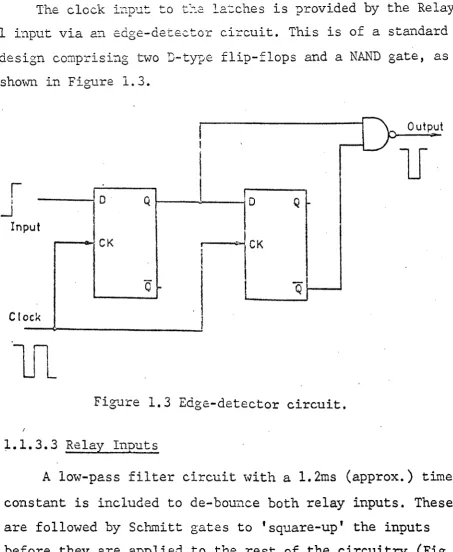
The clock hlPUt to t~;'2 l.e.'~ches is provided by the Relay
I input via an edge-detector circuit. This is of a standard design comprisi:1g two D-type flip-flops and a NAND gate, as
shown in Figure 1.3.
Output
1J
I
I..J
In
o· Q
!
I
put
CK
o Q
CK
I
Q
I-C( ock
I
lJ1
Fi~Jre 1.3 Edge-detector circuit.
1.1.3.3 Relay Inputs
A low-pass filter circuit with a 1.2ms (approx.) time constant is included to de-bounce both relay inputs. These are followed by Schmitt gates to 'square-up' the inputs before they are applied to the rest of the circuitry (Fig.
[image:14.529.34.488.65.617.2]1.4).
Figure
1.4- Relay
de-bounce circuit •Relay 1 is used to provide the clock input for the
control latch and Relay 2 to generate the Peripheral Request (PeRq) line of the handshake pair.
When set, the relay input (to the link) is connected to ground and when clear the input is floating.
1.1.3.4 Reset Input
Two reset inputs are provided, one under software control via the FM1600B and the other a manual input which must be taken to ground to effect a reset.
Upon start-up, the Gipop outputs will be in some indet-erminate state, with the result that Relay 2 may be set
thus generating a permanent peripheral request. This situation would not be rectified until the first Gipop scan were
performed, with the result that an interrupt error would be generated immediately.
To overcome this problem a latch is used to provide an enable control for the PeRq line. This latch may be cleared by either reset input and is not set until after the control word has been latched. Note, this requires that Relay 1 be
set at least once before the Relay 2 input can have any affect on the circuit.
1.1.3.5 Oscillator Circuit
A small oscillator circuit, running at ::: 30kHz, is included to provide the clock input to the control latches, via the edge-detector circuit. The circuit is as shown in Figure 1.5.
1.1.3.6 Bi-Directional Driver-Receivers
Sixteen bi-directional driver-receiver circuits are provided, each comprising two open-collector gates and two pull-up resistors (see Figs.
1.7 and 1.8).
The highway fromt1:2 also
'. "
l:.·...:.-l. eCl~·-c.·? c-::..
to the user
';:.'2.2 1 ir~k board (RO - R1S) and
(R20 - R3S) •. Hence, the user need not provide; 2.ny l~ull-"'..lp :;:-esistors on a peripheral board designed to operate with ths link.
-~- Vee·
330.(\.
330/\ 555
1
I
IITITr
Figure 1.5 Oscillator circuit and timing waveform.
1.1.3.7 Pmver Supply
The 1ir~k is provided '\-lith a self contained 5V @ lA power supply unit of conventional design (see Fig. 1.19). Note, the
OV
supply is separated from earth so as to avoid earth. loop problems with the FM1600B and other peripheral circuits.1.1.3.8 Power ~ply Consio.E::rations
The FH1600B uses a L~. SV supply voltage and no input should be allowed to go above this value. The TTL circuits' in the link, however, require a 5V supply and so care must
U 2:2 1 U13
010 5 6 1.. 03
®
DirU 22
\7
(0
16
13. 12 5
011 j ,})6
@Q
U22
I
5
19
012 11 10 12 U3 10
0)08,
gUn®In Sr Cc
U 22 10 20
9, 8 13 15 nun R 37
01 :3 11
Read
R38
9. 1 Write
6 2 4 5 12 10
3 11
U24 U24
RELAY 1
,
. .l,C1
8R46 13
4
5
6 Pe Rq
32
•
R40
. U22
U 231 4 rV"'13 27
3
cQ
£
c4'J~---D
Pe AcFigure 1.6 Overall circuit diagram for control section.
Vdd
DID 1
3
·01 1
5 2
001
6
13
1
2
6
t..
5
11
Pe DaD
(A)
Pe Do 1
Figure 1.8 Bi-directional drivers/receivers 8 - 15.
h. 4. 1..1/ s~~>f;';'J \., ~::, -'.' ::.o:.:..~:.:~~,:::t2Ci r:.::orl.1 the 5\l supply (Vcc)
of the link by the use of a diode (see Fig. 1.19) and this is used on any lines to or from the FM1600B requiring a pull-up voltage.
1.1.3.9 Mechanical Construction
All of the circuitry needed for the link is housed in a small aluminium box mounted on the laboratory wall in the Level 4 laboratory of the Electrical and Electronic Engineering Department, The City University, London. For mechanical details
see Figures 1.20 to 1.22.
1.1.4 Circuit Operation
The start of any sequence should be to reset the link hardware, and this can be achieved by taking either reset
input low. The data output word and relay control word
should now be cleared and a scan initiated so as to set all of the link inputs to a known state.
Once this has been done the required code word should be loaded into the Gipop data output word location (see
58090),
Relay 1 set and a second scan initiated. This causesthe code word to be latched into the control word latch and enables the PeRq output. The system is now ready to commence read-write operations (see Fig. 1.9).
For a read operation bit three 6f the control word must be low and for a write, it must be high. This signal is then
inverted and used to control the bi-directional latches. If the link is set for a read operation, then the relay control word should be loaded to set Relay
2
and positive-going external program interrupts should be enabled (n.b.the
FM1600B,
uses a negative logic conventi~n).A
scan isnow initiated with Relay
2
causing a peripheral request to be issued. TheFM1600B
then waits for the peripheral accept signal, which causes a program interrupt.The FM1600B
checksReset
U
Relay 1
~
Relay 2
~
Pe Rq
~
Pe At
~
0
~
\
Q
~
\
I
~
\
R/W
~
\
(A) (SI (e)
(A) Reset hardware
(B) Initiate scan to reset relays and data output
(C) Initiate scan to set Relay 1 and latch control word (D) System ready for use
Figure 1.9 Link set-up sequence •
.. 12
that the interrupt was valid and, if correct, reads the data, input word from the Gipop data area. Note, end of scan int-errupts are ignored.
The relay control word must now be loaded to clear Relay 2 and negative-going external program interrupts
enabled. A second scan is initiated which resets the periph-eral request line and again the FMl600B waits for the
peripheral accept signal via the interrupt input. If the interrupt is valid then the system is ready for the next transfer. This sequence continues until all words have been transferred (see Fig. 1.10).
For a write operation the sequence of events is very similar to that of the read operation except that now the data output word in the Gipop data area must be loaded before a peripheral request is issued. Also, the edges of the
peripheral request and accept waveforms have different meanings (see Fig. 1.11).
1.1.5 Operation with the FIOO System
The link was designed primarily for use as an interface between the FMl600B and FIOO systems. The following explan-ation of this link-up, although specific to the FlOO system, can be considered as a typical example of the use of the Gipop link.
The FIOO system is connected to the link via a 25-way
Cannon connector and a 25-way twisted~pair cable, approximately 1m in length. This cable is connected to the Gipop buffer
board of the FIOO which is described 'in a separate document (see Chap. 11.2).
A complete set of programs has been written to control the FMl600B and FIOO link-up (see later). These enable the user t,o specify the type of operation required (i.e. read
or write), a start address of a data area in the F100's
Reset
Relay 1
Relay 2
Pe Rq
Pe Ac
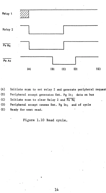
(AI IB) ( C) (0) ( E)
(A) Initiate sc.an to set relay 2 and generate peripheral request (B) Peripheral accep~ generates Ext. Pg It; data on bus
(C) Initiate scan to clear Relay 2·and Fe Rq
(D) Peripheral accept causes Ext. Pg It; end of cycle (E) Ready for next read.
Figure 1.10 Read cycle.
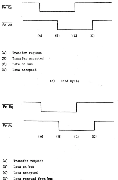
[image:23.529.44.464.85.850.2]Pe·Ac
______ I
(AI
(A) Transfer re~uest
(B) Transfer accepted
(C) Data on bus (D) Data accepted
. Pe Rq
\
Pe Ac
( A)
(A) Transfer request
(B) Data on bus
(C) Data accepted
CB) ( C)
(a) Read Cycle
( B) (C)
(D) Data removed from bus
(b) Write Cycle
( D)
( 01
Figure 1.11 Peripheral request and accept handshake lines.
[image:24.529.40.446.51.667.2]and the length of the block to be transferred. This is
normally performed under teletype control, the user receiving appropriate prompts. When these· three parameters have been entered the system is ready for use.
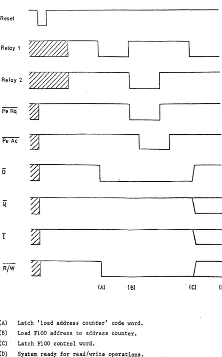
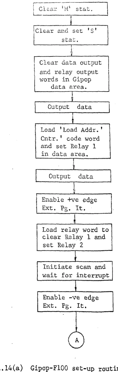
The link set-up-procedure is as explained earlier in the circuit operation description (sect. 1.1.4). In addition to the link set-up, the FIOO must also be set-up, which
requires that the FIOO address be written into an address register. To do this, a code word corresponding to the 'load address counter' code word for the FlOOis latched into the control latch and a transfer initiated to write the start address to the FIOO. The control word specified by the user
(i.e. read or write) is now transferred to·the control latch and both the link and the FIOO are now set-up and ready for use. The timing waveforms for the complete set-up sequence
.
.
are.as shown in Figure 1.12.
The read and write operations are performed in exactly the same manner as described in the circu~t operation section. These transfers continue until the number of transfers
specified by the 'length' input have been completed.
A complete set of program listings and flow diagrams is included fo~ this example as most of them will be
required for any application using the Gipop link; only the control and set-up (58080) programs need be changed.
The Gipop-FIOO delay routine (58085) is used to set a software delay of lOms (approx.) necessa~ to let the relay outputs settle before the program can proceed. This program is self expl~to~ as is the Gipop Data Area subroutine (58090) and no flow diagrams are included.
Reset
Relay 1
~
Relay 2
~
Pe Rq
~
I
Pe Ac
~
0
~.
I
Q
~
\
I
~
\
R/W
~
I
(A) ( B) . (C) (0)
(A) Latch 'load address counter' code word.
(B) Load F100 address to address counter.
(C) . Latch FIOO control word.
(D) System ready for read/write operatiQns.
Figure 1.12 FIOO set-up sequence.
[image:26.533.52.497.49.765.2]No
No
Output No text
'ERROR'
Output text 'READ OR WRITE'
Read chara from TTY.
No Yes
Yes
Set write flag
Yes Set read
I--~'"
flag
Yes
Stop 12
Output text 'M ADDRESS ?'
Read M addr. from TTY ,and
store
Output text 'B ADDRESS l'
Read B addr. from TTY and
store
Output text
'LENGTH? '
Figure l.l3(a) Control program for Gipop-FlOO interface.
Read length from TTY and
store
Output text
, - - - ' - t , READY'
No
No
Read chara. from TTY
Yes
Yes Jump to perform operation
Output text
'DONE'
Figure 1.13(b) Control program for Gipop-FIOO interface
(cont.)
N
CONTROL ?RO~RAM FOR ~I?OP/F100 INTERFACE - R.A.C. 1/7/77:
u
[1]V19=6
TEXT 1? 1E
READ OR WR I TE1 V19=5 "S555,1 "3.V21#tVNO=0 +195 V2=14 .. 2,V21#tVNO=0 +215 V2=5
.. 2, V 21#VNO=0 +210
"5,V21#VNO=O +197
V19=6
TEXT 1P 1E
ERROR -.. 1
[2JV19=6
TEXT 1P 1E
M ADDRESS?
V19=5
V23=O
"5100V11=V-21-1
V19=6
TEXT 1? 1E B ADDRESS?
V19=5
V23=O
"S100V12=V21 V19=6
TEXT 1P 1E
LENGTH '1 V19=5 V2J=0 "S100
V14-V21 [J]V19111
6
TEXT 1P 1E
REAOY
V19:a5
"S555,1
.. 4, V 21Ii!VNO-O +71
.. 1, V21HVNO-O
+197
# 1 #
'IC-CONT NUEd.
# #
. R-READ,_
·~.E-ENDt
# V1 =M ADDRu, 1 #
# #
I:V14-LENtlTH,1 .
l~INPUT ~(~O) OR E(ERROR),~.
"
,
.
[4]"58080 .
V19=6
TEXT 1P 1E
DONE
.. 1
[5]V19=4
V22=12
"S555.6
.. 1END A
'STOP 12.~.
, -I
; Cl~ar 1M' stat.
l
L - _ _ _
!Clear and set
is'
stat.
Clear data output and relay output
\vords in Gipop
data 2rea. Output: data
Load 'Load Addr. '
Cntr.' code word and set Relay 1
in data area.
Output
~
data,;
Enable +ve edge Ext. Pg. It.
load relay word to
clear Relay 1 and set Relay 2
Initiate scan and wait for interrupt
Enable -ve edge Ext.
Pg.
It. [image:31.534.121.368.38.817.2]A
Figure
1.14(a)Gipop-FIOO set-up routine (S8080).
Load data out word with 'M' addr. and
relay word to clear Relay 2
Initiate scan and wait for interrupt
Load 'M' control word to data out and relay word to
set Relay 1
Output data
Jump to read-write routine
Figure 1.l4(b) Gipop-F100 set-up routine (cont.).
N
58080 ~IPOP/F100M SET-UP ROUTINE - R.A.C.
1/7/77:
U VN3=V10,N3-1 VN3=N1,NJ-1 VN3=N2,N3-1 QN320=O QS320=O QS320f!l£0 N1=VNO AS8090,2 VN1=O VN1=O,N1+1 V10=0 V10[1]~O ~S8084 "S8085 N1=VNO AS8090,2 VN1=9 VN1=1,N1+1 V10[1]#O ~S8084 "S8085 V10[2]=O N1=VNO AS8090,) VN1=2 V10[1]=0 "S8084 "S8085 V10[2]NO N1a VNO
ASBOgO,2 VN1=Y11 VN1=O.N1+1 V10(1)=O "S8084 "S8085 N1=VNQ AS8090,2 VN1-Y2 YN1-1,N1+1
,~CLEAR DA TA OUT? UT \JOROt,.
,ICLEAR RELAY OUTPUTS:j 0
,"'SET INTERRUPT FL.AQ,"1.
I~OUTPUT DATA
t;. .
,"oWA I T FOR RELAys TO SETTLE~ I
,"'0 A TA=LOAD ADDR CNTR CODE WD,~.
"
,
.o .. SET RELAY 1. J
"
"
,OUTPUT DATAIJ'
"
,"CL.EAR REL.AY 1 JSET RELAY 2, i 0
,'IINI TIATE SCANt'J,
IENABLE -VE EDQE EXT p~ IT~'
,'VN1=-M ADOR,",·
,'''.cLEAR RELAY 2~
"il NI TIATE SCAN~,
I ,
"VN1-M CONTROL WORDd'
, E '
1ST RELAY 1,_,
V10[1]#O
.. S8084
"'S8085
"58088 N2=VN) VO=VO,N)+1
N1=VN3 VO=VO,N3+1 V10=VN3.N3+1 ... L
END
S
8080
~ "
t RESET FLA~· i '
" OUTPUT 'CODE WORD.·!· ~
,~JUM? TO READ/WRITE ROUTINE~'
qIPOP/F100M SET-UP ROUTINE - R.A.C.
1/7/77:
No
Clear test word
Set up for scan
Clear
'F'
stat. if setStart scan
Yes
Restore link
Output text
'*QF SET'
Stop 10
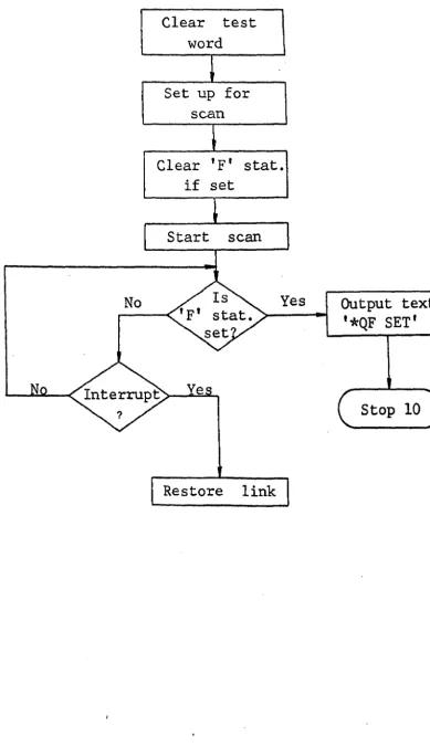
Figure 1.15 Initiate scan and wait for interrupt (S8084).
[image:35.543.92.482.52.729.2]N
58084 INITIATE SCAN AND WAIT FOR INTRRUPT - R.A.C.
1/7/77:
u
VN3=N1,N)-1 N1=VNO
AS8090 VN1=O
N1=V~O
IB320,DP VN1=VNO AS8090
VN1~VNO,N1+1
AS8089
QF320=0
Q~1) 2~#O
[O] ... 1,QF320#O .. O,V10[1]=O
N1=VN3 VO=VO,N3+1
"L.
[1]V19=6
TEXT 1? 1E • QF SET
V19=4
V22=10
[10]"'5555,6
.. 10 END
~ C L.EAR TEST WOR D\~ ,
~ SET UP SCAN,."
"
:'SET UP INT ADDRI~'
l~Cl.EAR F STAT IF SET!i I
~l N 1 TIATE SCAN~:'
\" JUMP TO DRUID STOP IFF STAT SET1~j'
"WA I T FOR INTERRUPT,", I ' .
S
8084
INITIATE ,SCAN AND WAlT FOR INTERRUPT - R.A.C.
1/7/77:
Enable +ve edge Ext. Pg. It.
Load relay word to set Relay 2 (and clear Relay 1)
Initiate scan and wait for interrupt
~
Enable -ve edge Ext. Pg. It.
r--_---.;N;.;.O~-<£:>-=y::..;;e;.;;s~--..,
Load relay word to clear Relay 2
Initiate scan and wait for interrupt
Copy data from data input. word to store using 'B' addr. as
pntr. .
?
Load data out word with data and relay word to clear Relay
2
Initiate scan and wait for interrupt
Increment 'B' addr.
---~ ~.---~
pntr.
Decr. length of count \
No
Ads, yes
~---< In-out Restore link-,
?
Figure
1.16
Gipop-FIOO read-write ·routine(S8088).
N
s8088 QIPOP/F100M READ/WRITE ROUTINE - R.A.C.
1/7/77:
u
VNJ=V8,NJ-1 VNJ=V12,NJ-1 VN3=V14,N3-1 VNJ=N1,N3-1 VN3=N2,N3-1 V14=V14-1 [1jV10[2]=0 N1=VNO AS8090, JVN1=2 V10=0 "S8084. "S8085 V10[2]~0 "2,V2-10>O N1=VNO AS 8090,) VN1=0 V10[1]=0 "S8084 "S8085' N1·VNO AS8090,1 V8-YN1 N1=V12 ' YN1-Y8
..
) [2]N1-YNQ AS8090,2 N2=V12,VN1-YN2&VN2 YN1=O,N1+1 Y10[1]=0 "S8084 "S8085 [)]V12=Y12+1 .. 1,Y14-V14-1>0 N2:=aVN) VO=VO,N)+1 N1=VN) VO=VQ,N)+1 V14=VN).N3+1V12=VN3,NJ+1
V8=YNJ,NJ+1
S 8068,
,
. ,ENABLE +YE EXT PQ ITL'J'
tCLEAR REL.AY 1; SET RELAY 2:~· tlNITIATE SCAN,~
, I '
, ENABLE -YE EXT PQ Tl j ,
,'JUMP IF
WRI TE REQUIREDt,,'CL.EAR RELAY 21~'
.'INITIATE SCAN0·
, A '
· V8-1 NPUT 0 TAli.
,
,
· N1-B ADDR,i ° .', ED'
,DATA STOR I.: •
tVN1-0UTPUT DATAt!· ,
2~
· CL.EAR REL.AY i! •
, A '
0, INI TIATE SC Nt-.oj·
,
tlNCREMENT B DATA POINTER,~ ° /I
,'CHECK FOR ALl. WORDS OUTPUT,,·
QIPOp/F100M
READ/WRITE ROUTINE -R.A.C.
1/7/77;
No
No
Output text 'Interrupt error'
Stop 14
No
Reset 1M' stat.
Yes
Yes
\
Yes
'---4I-t Read test
word~-Output text 'Test Word
Error'
. Stop 12
Set interrupt flag
. Figure 1.17 Gipop-FI00 interrupt routine (58089) .
N
58089 ~lPOP/F100M INTERRUPT ROUTINE - R.A.C.
1/7/77:
u VNJ=V19.NJ-1 VNJ=N1,NJ-1 QM)20=O N1=VNO 18)20,5':4 "J,VN1[OJ~O "S,VN1[7]UQ [7]Q2=O V19=6
TEXT 1P 1E
• INTERRUPT ERROR
V1g-4 V22=14
"S555.6
(5)N1=VNO18320,
sw
..
6,VN1[6)~0"1,V10[2]#Q [8)N1=VNO
AS80g0
.. 2,VN1~VNO~O
OCT 00177777
V10[1]UO [J)Q2-0 .. 4[6]"7,V10(2]-0
.. 8 [2]Q2-0 V19-6TEXT 1P 1E
• TEST WORD ERROR
V19=4 V22=12
"5555,6
[ 4]N1-YN) VO=VO,N)+1 V19-YNJ,NJ+1 S 8089."·EN
"
0 OF· SCAN,
IN TERR UP T 1 ~ .,£XT PG IT 1.
,
,
. STOp 14··\.
."CHECK TEST WOllO ALL ONESI"j.
."SET INT. FLAG . ..!·
!LEADINQ EDQE INT. REQD.7~.
, 2'
,STOP 1 I •
~IPOP/F100
INTERRUPT
ROUTINE - R.A.C.1/7/771
N'- .' ' . '
58085 ~IPOP/F100M DELAY ROUTINE - R.A.C. 1/7/77; U
VNJ=V9,NJ-1 V9=VNO
OCT 02000 .4110115 DELAY APPROX'~'·
[1] .. 1,V9=V9-1>0 V9=VNJ,NJ+1 .. L
41 41
. LOOp TILL COUNT = ZEROt::l·
END
s
8085
~lPOP/F100 DELAY ROUTINE - R.A.C. 1/7/77;
N
58090 ~IPOp DATA AREA - R.A.C.
1/7/77;
U+0 +0 +0 +0 +0 .
END
S
:'TEST WORD·-.
4IDATA INPUT WOR 0,41
'DATA OUTPUT WORD,~:
~.
,
. RELAY 41 CONTROL \iORDI:i' , 1 SWI TCH INPUT WORD,.,
8090
~lpOp DATA AREA; - R.A.C.
1/7/77;
1.1.6 Miscellaneous Details 1.1.6.1 Components List Resistors
All 3300 ~ ±5%
except:-R17,R19 1200 ~ ±5%
R36,R41,R42,R46,R50 Capacitors
CI,C2 IO~F elect. 25v C3,C4 2.2nF ceramic
4.7k
bv
±5%C5 .047~F polyester 150v C6,C7,C8 O.I~F ceramic
C9 4700~F elect. 25v CIO 0.47~F polyester
Semiconductors
DI Si diode OA200 D2 - D5 Si diode OA200 D6 Si diode IN4004 REG1 5v regulator 7805
Integrated Circuits
U1,U2,U5,U11,U12,U13,U15,U23,U25,U26 SN7438
U3 SN74175
U4,U24 SN7474
U6 ZN344E
U14 SN7400
U16 NE555
U21 SN7413
U22 SN7404
Miscellaneous
Tr 1 - Mains transformer 4.5v
@
2.2A, 4.5v@
2.2A Fs 1 - Fuse (2A anti-surge)+
holderSk 1 - 25-way Cannon connector Sk
2 -
3
pin mains socket (Bulgin)Sw 1 -
Mi~-toggleDPDT
Lp 1 -
6v sub-min indicator (amber)
o
col
l - - . _ _ _ _ _ _~I
<\ '---
---~
o
o
[I]
IT]
Ie .... 11
Figure 1.18 Component
layout.
I
Fs1 Tr1
l
III
Sw1
0
A S,
REG.1
0+5 V
N 0 C
C9 Lp 1
T
C10~R50
t 0 6I
E
W
VI
OV
+ 5 V o . , 9 ,~ Vee
1 01
C6 C7 C8
L -_ _ CII>_ V dd
;. OV 0 '
' 6
po- 0 VE.C.l - 32-way edge connector
(A) 20-way printed circuit connector (B) - 20-way printed circuit connector
His
1 - 4°C!W heatsink 1 X R.S. Type C stripboard2 X Tag strips
1.1.7 Connection Lists 1.1.7.1 Cannon connector
1 Pe Da 0
2 Pe Da 1
3 Pe Da 2
4 Pe·Da 3
5 Pe Da 4
6 Pe Da 5
7 Pe Da 6
8 Pe Da 7
9 Pe Da 8
10 Pe Da 9
11 Pe Da 10
12 Pe Da 11
13 Pe Da 12
14 GND
15 Pe Da 13
16 Pe Da 14
17 Pe Da 15
18
·Pe Rq19 Dir In
20
Q
21 In Sr Cc
22 Pe Ac
23
Reset (Ext.)
24
Enable (GND)
25
·GND
1.1.7.2 Board edge connector 1
2
3
4
Vee DI 0 Dr 1
5 DI 2
6 DI 3
7 DI 4
8 DI 5
9 DI 6
10 Dr 7
11 GND
12 Vee
13 Dr 8
14 Dr 9
15 Dr 10
16 Dr 11
17 Dr 12
18 DI 13
19 DI 14
20 DI 15
21 GND
22 Vee
23 t S t stat. 24 Relay 1
25
26 Reset (Ext.)
27 Pe Ae
28 Relay 2
29
-30
31 GND
32 Pe Rq
(Note: DI means data input from FM1600B)
1.1.7.3 Printed circuit connectors
Connector (A) Connector (B)
1 Pe Da 0 1 DO 0
2 Pe Da 1 2 DO 1
3 Pe Da 2 3 DO 2
4 Pe Da 3 4 DO 3
5 Pe Da 4 5 DO 4
6 Pe Da 5 6 DO 5
7 Pe Da 6 7 DO 6
8 Pe Da 7 8 DO 7
9 Pe Da 8 9 DO 8
10 Pe Da 9 10 DO 9
11 Pe Da 10 11 DO 10
12 Pe Da 11 12 DO 11
13 Pe Da 12 13 DO 12
14 Pe Da 13 14 DO 13
15 Pe Da 14 15 DO 14
16 Pe Da 15 16 DO 15
17 17
18 Dir In 18 Ext. Pg. It.
19 Q 19
20 In Sr Cc 20
(Note: DO means data output to the FM1600B)
1.1.7.4 Tag-strip connectors
'rag-strip 1 Tag-strip 2
1 Pe Da 0 1 DO 0
2 Pe Da 1 2 DO 1
3 Pe Da 2 3 DO 2
4 Pe Da 3 4 DO 3
5 Pe Da 4 5 DO 4
6 Pe Da 5 6 DO 5
7 Pe Da 6 7 DO 6
8 Pe Da 7 8 DO. 7
9 Pe Da 8 9 DO 8
10 Pe Da 9 10 DO 9
11 Pe Da 10 11 DO 10
12 Pe Da 11 12 DO 11
13 Pe Da 12 13 DO 12
14 Pe Da 13 14 'DO 13
15 Pe Da 14 15 DO 14
16 Pe Da 15 16 DO 15
17 17
18 Pe Rq 18 Ext. Pg. It.
19 Dir In 19
20 Q 20
21 In Sr Cc 21
22 Pe Ac 22
23 Reset (Ext.) 23
-24 24
25 25
26 ' 26
27 27
1_
£5.1.
62.5 -..I , . . 62.5 r-- .\ .. 25.1
I IJ'!~ N1-.-
-(-
)
\0.-.(
J
-N
+
[1-.
iJ
+
Ni
J ~.
~I
82.5
1-
82.5 5716 11' 16
.. tit
-11 -11-25
I I I
~~
-+**'ffl
+.+
1 --\0
en
.-
..-+
l-I ,
+
en..-+.+
L--,-
-+-
-1-~
0
I '
I
22I
321
37.5.1
~ ~11
11I
32 . - . •-:r
~
--L
I~
67L
54 .\ • • "1' one: • 0." -rene ....
. , 20 C~ se - ::-CG.ln ... 1 F1~ure J.. . ..
lQ.
-4~
~
U')
~
i
en
....
<?-~
t
-:t
~t
-
t-~If)
N
t
~
r--~
o o
N
1
I
I.I
0:;1
-enl
I
I
I
1::-
- " ,-
It)-Figure 1.21 Case - inner support
di~ensions.
...
c::(
0
r--
l-...
l-
----o.~
I=l
0 '(y
t - -~
0
... N
CJ) CJ)
t-
....
t
-0
LQ.
&
I ... 1/1 U. ~ "U .... 0 0 en 01 ClI o:: 0 i 0 L. ~
~~
1.
I... ~ LLJ J ... &.: t-t -l 0\ U
--,
1Figure __ l.22 Case - internal layout.
1.2 User G'~id'2
1.2.1 Introduction
The Gipop (ge~-~eJ:.-c::.l inpl:t-outp'u.t) link is basically a sixteen-bit bi-directional driver-receiver unit attached to the Gipop higY~\Nay of the Fl'11600B computer. The Gipop unit is a peripheral of th.e FM1600B and is well documented
elsewhere ~1. The link and associated programs are designed to make the Gipop unit easy to use.
The Gipop link is intended primarily for use as an interface between the FM1600B and the FlOO microcomputer system, but may be easily adapted for general use by the provision of a suitable control program, and some minor
changes to the subroutines described in this document. In addition to the sixteen-bit bi-directional data highway, three latched outputs are supplied for control purposes and a handshake pair included to provide a
comprehensive interface facility.
The circuit has been designed in such a way that the control word may be latched from the Gipop highway before
the first request is issued via the handshake lines. In this manner, the'control word is stable at the interface before
any data transfers are initiated.
1.2.2
Electrical Specifisatio~All inputs and outputs to and from the link are TTL compatible. The use of open-collector drivers is recommended to' drive the highway between the user peripheral and the link. The data highway is pulled-up by the link (via 330Q to Sv)and so no pull-up resistors need ,be provided by the user.
The, control lines are driven by open-collector gates and should. be pulled-u? by the user via a ~uitable circuit
(see Technical Description). Pull-up resistors are provided
on the link ,board but are not connected
tothe Vce
supply.They may be
connected
if
desired but
their useis
notrecommended [2] •
The operating speed is limited to half the maximum scan rate available for the Gipop unit and the settling time
required by the Gipop link circuits. This results in a maximum transfer rate of ::::: 70Hz or one transfer per 15 ms.
1.2.3 Gipop Set-Up
The following is a brief description of the required configuration of the Gipop unit when used with the link.
The data area for the link (S8090) is arranged in the following
order:-o
Test word1 Data input word
2 Data output word
3 Relay control word 4 Switch input word
Performing the scan in this order ensures that the data input and output words are stable before any peripheral
activity is instigated via the relay outputs. The switch input word is included for the sake of completeness and to accommodate any future developments.
The order of the boards in the Gipop half-shelf module of the FM1600B should be as given in Table 1.2.1.
Two switches are included on the back of the Gipop
half-shelf (in the back of the FM1600B) , one a rotary switch (FIN WD) and the other a toggle (SCAN). The FIN WD switch should beset to the 3 position (4 if switch input required) and the SCAN switch to the INT position.
Numerous jump leads are required on the Gipop patch board (at side of FM1600B); the complete set-up for this is as shown in Figure 1.2.1.
1.2.4 Program Requirements
A complete set of subroutines has been written to operate the Gipop link. The user need only write a control program and a set-up routine for the peripheral attached to
the link. For examples of these pr6grams and complete
explanations of the operating routines the reader is referred to Ref. 2 •
The basic set-up requirements of the operating routines is as
follows:-V2
=
code word (i.e. control word output) VII =V12
=
V14=
peripheral address FM1600B start address number of transfers
Note, at the end of a transfer sequence these registers are returned to the user in an uncorrupted state. However, during the excution of the transfers V12 is incremented from its initial starting point and V14 is decremented to zero. Once at zero, the registers are restored and control returned to
the user program. The programs are designed for block transfer operation and if the FM1600B address is required to remain constant then block transfers of length one must be performed (or the read-write routine (S8088) modified). The following subroutines are available to the user:-58080 - Set-up routine
No. of words -
SO
Entry point - 0
Registers destroyed - none
Subroutines called - 58084, 58085, 58090
This·routine performs all the necessary set-up operations required for the use of the link with the
FIOO
system.58084 - Initiate scan
and
waitfor
interrupt No. of words - 28Entry
poipt -
0
Registers destroyed - VIO, V19, V22 Subroutines called - S8089, S555, S12
This routine initiates the Gipop scan and loops on a flag in VIO, waiting for an interrupt.
S8085 - Delay routine No. of words - 6
Entry point - 0
Registers destroyed - none Subroutines called - none
This routine generates a 10ms (approx.) delay by means of a count-down loop, necessary to allow the Gipop relay outputs to settle before the next operation is started.
S8088 - Read-write routine No. of words - 45
Entry point - 0
Registers destroyed - VIO
Subroutines called - S8084, S8085, S8090
This routine performs the data transfer portion of the scan.
S8089 - Interrupt routine No. of words - 55
Entry point - 0
Registers destroyed - VlO, V22
Subroutines called - S8090, S555, S12
This routine checks for valid interrupts and that the Gipop test word has been transferred correctly.
S8090 - Gipop data area No. of "''lords - 5 Entry point - N.A.
Registers destroyed - none Subroutines called - none
This is a five word data area used
by
the Gipop unit during data transfers. The area is arranged asWord 0 - Test word
1 - Data input word 2 - Data output word 3 - Relay control word 4 - Switch input word
1.2.5 Mechanical Details
The Gipop link is contained in a small aluminium box attached to the laboratory wall in the level 4 laboratory
of the Electrical and Electronic Engineering Department, The City University, London.
The link is provided with a self-contained power supply in which OV and GND are isolated. A switch and indicator are included with the supply.
Connection to the link is by means of a is-way Cannon connector mounted on the top of the case. The connections for this socket are given in the Technical Description, section 1.1.7.1.
Position Board No. Function
1 189 Control board
2 020 Control board
3. 845 Control board
4 079 Voltage input interface
5 079 Voltage input interface
6 023 Voltage output interface
7 022 Relay output interface
8 - 12 Not used
Table
1.2.1
Board order in the Gipop half-shelf module.VOLTAGE INPUT VOLTAGE OUTPUT
00--0
0
00--0
0
0--0
0
0-0
0
0--0
0
0
0
0
0-0',
0
0
0
0
0--0
0
0
0--0
0--0
0
0
0----0
0-0
0
0
0
0
0--0
0
0
0
0
0--0
0
'0
0
0
0-0
0
0
0
0
0 - 0
0
0
0
0
0-0
0
0
0
0
0 - 0
0
0
0
0
0 - 0
0
0
0
0
0 - 0
0
0
0
0
0
0
0
o
'0
0
17
0
0
0
170
0
0
Data input
SWITCH INPUT RELAY OUTPUT
0 0 - 0
0
00
0
0
0---0
0
0
0
0
0-0
0
0
0
0
0---0
0
0
0
0
0---0
0
0
0
0
0-0
0
0
0
0
0--0
0
0
0
0
0---0
0
0
0
0
'0---0
0
0
0
0
0-0
0
0
0
0
0-0
0
0
0
0
0-0
0
0
0
0
0-0
0
0
0
0
0 - 0
0
0
0
0
0 - 0
0
0 - 0
o '
S-line0
0
0
0--0
O.
Ext. Pg. It.17
0
0
0
17
0
0
0
Data output
Figure 1.2.1 Gipop patch board
connec~ions.1.20 6 Use of the link in the FM1600B-FIOO interface
This section explains the use of the control 'program and set-up re~uirements of the Gipop link when used with the FIOOM microcomputer system as a peripheral.
The link is connected to the F100l1 via the Gipop buffer board [3][4] which is in turn connected to channel 1 of the FIOOM's input-output controller
(roc).
The peripheraladdress is entered into a register in the IOC as the start address of a block of FIOOH store. Note, a pre-increment is performed on this register and so the user must set VII to
the start address minus 1. Before the address register may be loaded it must first be accessed via the F100M's front panel, to initialize the circuits from their start-up
settings. To do this the user must access location 32763 (all handswitches set except 2 and 15); the data loaded is irrelevant. The FIOOM and link are now ready for data
transfers.
The control program requests the various parameters from the user via the teletype by a series of prompts. The first of these is 'Read or Write' to which the user
replies:-R - replies:-Read W - Write
C - Continue (with the settings from the previous run) E - End (jump to Stop 12).
The
'c'
command jumps the control program straight to the 'Ready' state, by-passing the rest of the set-upprocedure. This can be ext!eme1y useful for test purposes. If any input, other than the above four, is entered, 'Error' is output on the teletype and the 'Read or Write' prompt repeated.
Note, all characters or character strings are terminated with a space.
Next, the 1M Address', IB Address' and 'Length' are
requested and the corresponding values are entered in decimal. 'Ready' is now output, to which the user may
reply:-G - reply:-Go
E - Error. Return to 'Read or write' prompt to re-enter parameters.
If neither of the above characters are entered the 'Ready' prompt is repeated.
When 'G' is entered the requested operation is performed and when completed, 'Done' is output and the 'Read or Write' prompt re-issued.
1.2.7 References
1. Gipop Manuals, Ferranti Ltd., Oct. '71
+
updates. 2. Gipop.link - Technical Description, Internal report,R. A. Comley, July '77.
3. Gipop Buffer - Technical Description, Internal report,
R. A.
Comley, July'77.
4.
Gipop Buffer - User Guide, Internal report,R. A.
Comley, July '77.2
Gipop Buffer
1. Technical Description
2. User Guide
2.1.1 Introduction
The Gipop (general input-out?ut) buffer is a general purpose data channel for the F100H microcomputer system. It
is basically a sixteen-bit bi-directional input-output buffer designed, primarily, for use in the FM1600B and F100M inter-face, but may be of general use whenever a slow peripheral must be interfaced to the F100M system (see Fig. 2.1).
The sixteen input-output lines are latched on the buffer board which relieves the user of the timing restrictions
imposed by the F100M. The user may select the handshake response time by the use of two monostable circuits. At present, it is set to 2ms (approx.) for use with the Gipop
link and FM1600B.
The buffer is connected into channel 1 of the input-output controller (IOC) of the F100M system and all data
transfers take place under direct memory access (DMA) control. For this purpose, three control lines (Dir,
Q,
In Sr Cc) and a peripheral request-accept handshake pair are provided. The three control inputs are enabled via a fourth input (Enable) which is active low (Ov). This ensures that when not in use(i.e. Cannon plug disconnected) the board is disabled.
All input-output between the Gipop buffer and peripheral devices is via a 25-way twisted-pair cable and a 25-way
Cannon connector.
2.1.2 Design Considerations
The fundamental design consideration of the Gipop
buffer was to provide an asynchronous interface between the FIOOM and a peripheral, and in particular for the ~nterface between the
FIOOM
and theFM1600B.
TheFIOOM,
however, is constrainedby
a 'time-out' on peripheral transfers (50~s max.) and hence the need for the buffer board. The GipoplJ1
w
Oir
Q
In Sr C
En
Pe Rq
Pe Ac
Reset
Da ta Bus
(16 bils)
GIPOP t. CHANNEL F 100
BUFFER 1.0. C. SYSTEM
- - - -~
buffer permits asynchronous transfers at both the FIOOM and peripheral interfaces.
The basic form of the handshake at either interface is as shown in Figure 2.2, but the time scale for a peripheral and the FlOOM will generally be very different. The complete handshake sequence for both the FIOOM and a peripheral will be as shown in Figure 2.3.
For a read cycle, the attention request (AtRq) (or peripheral request (PeRq) from the peripheral) causes an
immediate peripheral request to the FIOOM. Upon completion of the FIOOM read cycle (i.e. PeAc returned high) the
requested data are available and, after some time interval T1 , attention accept (AtAc) is issued. The time interval T1
is governed by the response time of the peripheral and set by a monostable. After attention accept has been issued,
the peripheral then completes its handshake sequence w~th the buffer board.
For a write cycle, the rising edge of AtRq must be used to issue PeRq to the FIOOM to ensure that the data to be
written are available at the start of the FIOOM cycle. Again, a time delay, T2 , should be included to ensure that AtAc is not cleared too quickly after AtRq has been reset.
Froman inspection of Figures
2.2
and2.3
it is apparent that some form of latch is required to hold the input-output data during transfers, as in both the read and write cycies the transfers to or from the FIOOM take place with the data bus in some indeterminate state. To overcome this problem, . a directional latching system was included in the bi-directional driving circuitry (Figs. 2.14 -' 2.17).The complete control circuit to decode and generate the necessary timing signals is given in Figure
2.13.
Pe Rq
Pe Ac
(A) (B) ( C) ( 0)
(A) Transfer request
(B) Transfer accept : data on bus (C) Data accepted
(D) Data removed : end of cycle
(a) Read cycle.
Pe Rq
l~
______ --,
Pe Ac
..
IA) ( Bl ( C) (0)(A) Transfer request : data on bus
(B) Transfer accept • • data accepted (C) Data removed
(D) End of cycle
(b) Write cycle.
Figure 2.2 Handshake timing waveforms.
At Rq
At Ac
l. _ _ _ _ _
~
-..
...Pe Rq
PeAc
\~
__~
(a) Read cycle.
At Rq
~
________________~
At Ac
I
T2
--
..
Pe Rq
Pe Ac
(b) Write cycle.
Figure 2.3
Perip~eraland FIOOM relative timing waveforms.
2 . 1 • 3 C
---
i ':' c,~~ i t~.,,~ ,.~: , r: _l.. ,.--:...~
2.l.3.1 Cmtr2} ir.:::,.,t:;
..
---~-Three control i~puts a~e required to specify the type of D1'1A, operation required (2·2e Table 2.1) and these are
received and buffered as showJ in Fi?ure 2.4. An enable input o is also provided so tha.t ths 'Duffer board is effectively
disabled when unpluggec from the peripheral.
2.1.3.2 Read-write control
This is decoded from two of the three control inputs and is used to control data direction and set the handshake sequence within the Gipop buffer circuits. The circuit is as shown in Figure 2.5.
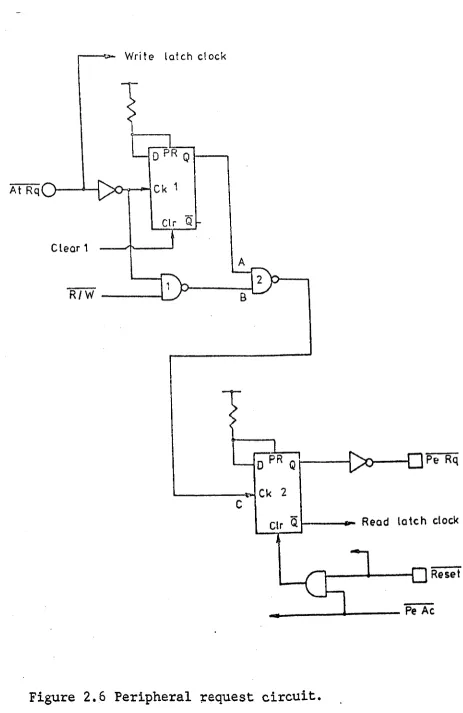
2.1.3.3 Peripheral request circuit
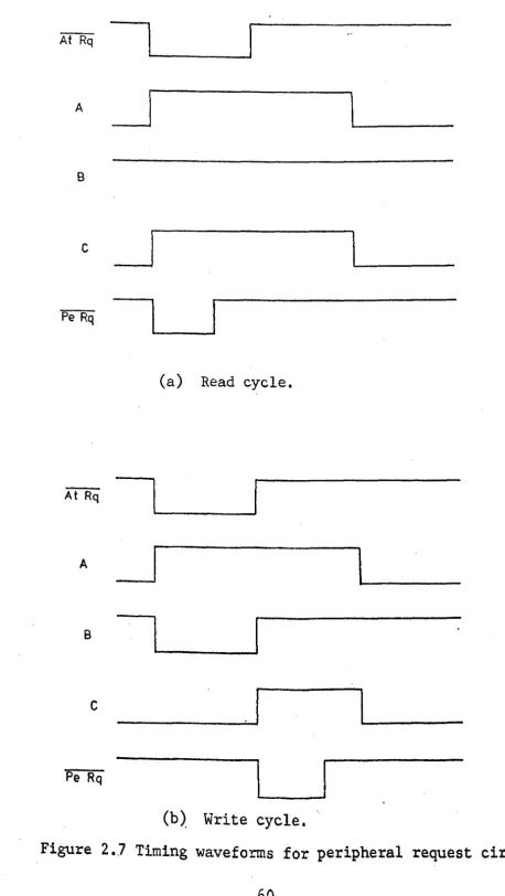
The route taken by attention request to D-type flip-flop 2 and thereby to the peripheral request output is determined by the state of the read-write input applied to NAND 1. This input is low for a read operation and high for a write. Hence, for a read operation AtRq goes via flip-flop
1 to clock flip-flop 2 and set PeRq on the first edge (trailing) of AtRq. For a \vrite operation, AtRq goes via NAND gates 1
and 2 but no signal reaches flip-flop 2 until AtRq returns to the high state (see Figs. 2.6 and 2.7).
Flip-flop 1 is cleared at the end of each transfer by the clear 1 signal (see later) and flip-flop 2 by the
peripheral accept signal. The main reset input is also taken to this input to ensure that
PeRq
is cleared when theFIOOM
is reset.
2.1.3.4 Peripher8.1 acc.eJ2.!:.
To ensure that the peripheral request signal is not
330.n.
In Sr Cc
19
11 30
In
3'3nF3'3 Oil
Q
18
34
:r:
33nF1 26
3
En
Figur~ 2.4 Control inputs.
In Sr C C - - - - f (from Read F 100)
Dir
Write
Figure 2.5 Read-write control.
..- Write latch clock
C tear 1
A
R/W ----L~
Pe Rq
L----~Ck 2
c
Clr Q ~---I""'" Read la1ch clock
ReSeT
..
---~~---~
Figure 2.6 Peripheral ~equest circuit.
[image:68.570.67.530.56.769.2]A
B
c
Pe Rq
(a) Read cycle.
AtRq
l~
________
~
A
11--_
B
I
c
Pe Rq
1
(b) Write cycle.
Figure 2 •
.7Timing waveforms for peripheral request circuit •
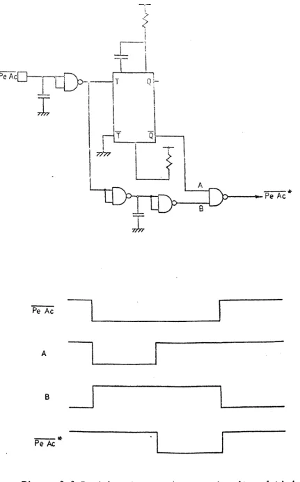
[image:69.576.58.516.37.849.2]cleared too quickly upon receipt of the, peripheral accept signal, a monostable is included. This delays the PeAc signal by O. 2,us (approx.) (Fig. 2.8).
2.1.3.5 Attention accept circuit
The mode of operation of this circuit is determined by the state of the read-write input. For a read operation the PeAc input causes a trigger signal to be generated which is applied to a monostable input (Figs. 2.9 and 2.10). This is set to give a delay of 2ms (approx.) after which time a D-type flip-'flop is clocked to generate the attention accept
-signal. For a write operation the trailing edge of the AtRq input causes the trigger pulse to the monos table to be_ generated, thereby issuing attention accept before peripheral request is issued (or peripheral accept received).
Attention accept is reset via the clear 1 input to the , flip-flop.
2.1.3.6 Clear 1 circuit
This circuit is used to reset the attention request and accept flip-flops and its mode of operation is also controlled by the state of the read-write circuit. For a read cycle, the AtRq input generates the trigger input to a monos table set to give 2ms (approx.) delay. The output from this monostable then causes the clear 1 signal to be generated (see Figs. 2.11 and 2.12). For a write cycle, the PeAc input causes the clear I signal to be generated. This ensures that clear I is generated at the correct time for both read and write cycles. The external reset (from the FIOOM) is also gated into the clear I circu~t to ensure that all flip-flops are reset when
the processor ~s reset.
Pe Ac
A
B
- *
Pe AcI
I
0:-
\. :- -
..
n----t.-Pe Ac
Figure 2.8.Peripheral accept' delay circuit and timing waveforms.
[image:71.571.49.481.54.748.2]At Rq---.:>---\
T
·~.)--Lrr[-,
.1
VJ--+---'
Pe Ac - - - - i - - - L J
c
T Qr---~Ck
o
elr Q
Clear 1
Figure 2.9 Attention accept circuit.
[image:72.586.54.503.78.793.2]--- --.-._---_. ---_ .•.
_---Fe Ac
i
I
A
~
B
I
IU
c
n
o
At Ac
a) Read cycle.
AtRq
~
A
r
B
c
o
At Ac
1
b) Write cycle
Figur~
2.10 Timing waveforms for attention accept circuit.
64
PeAo:---'
J
.c-;b
I'
c
} - - - - Clear 1~--IT QI----+--{
" - - - '
Reset
Figure 2.11 Clear 1 circuit.