Reprinted with permission by SAE © 2017 SAE International. Further distribution of this material is
not permitted without prior permission from SAE
Sztykiel, M., Fletcher, S., Norman, P., Galloway, S., & Burt, G. (2016). Modular and reconfigurable
transient modeling and simulation design support tool for MEE/MEA power systems. Paper
2016-01-2031
Modular and reconfigurable transient modeling and simulation design support tool
for MEE/MEA power systems
Author, co-author (
Do NOT enter this information. It will be pulled from participant tab in
MyTechZone
)
Affiliation (Do NOT enter this information. It will be pulled from participant tab in MyTechZone)
Abstract
There is a well-recognised need for robust simulation tools to support the design and evaluation of future More-Electric Engine and Aircraft (MEE/MEA) design concepts. Design options for these systems are increasingly complex, and normally include multiple power electronics converter topologies and machine drive units. In order to identify the most promising set of system configurations, a large number of technology variants need to be rapidly evaluated.
This paper will describe a method of MEE/MEA system design with the use of a newly developed transient modeling, simulation and testing tool aimed at accelerating the identification process of optimal components, testing novel technologies and finding key solutions at an early development stage. The developed tool is a Matlab/Simulink library consisting of functional sub-system units, which can be rapidly integrated to build complex system architecture models.
This paper will demonstrate this functionality by applying the tool to assess the suitability of various designs of active power converter circuitry for use with an example MEE/MEA network. Three aspects of the converters’ performance will be considered in order to assess this suitability: efficiency, power quality and fault tolerance. The example case studies will demonstrate the adequacy of the selected variant designs as well as the system level impacts of design decisions.
This will enable system designers to rapidly identify variant configurations of electrical components at early design stage that satisfy MEE/MEA system requirements.
Introduction
As the More-Electric Aircraft (MEA) and More-Electric Engine (MEE) concepts progress [1,2], the electrical architectures on the next generation of aircraft will undergo significant changes. These concepts will see an increasing number of non-propulsive systems operated with the use of electric power in order to facilitate a range of aircraft and engine level benefits.
In order to accommodate different sizes, functions and locations of these non-propulsive electrical systems, the electrical architecture must be carefully designed to ensure the efficient and reliable transmission of electrical energy.
Today, concepts for mixed dc and ac power systems are of increasing interest [3]. These designs often combine dc transmission with ac generation. In such network configurations, power electronics converters act as the interfaces, which transform the required amount of electrical power between ac and dc sides.
The design options for these systems are increasingly complex, driven by a broad range of different technology solutions for electrical components available on the market. Various engineering studies are required to properly identify an optimal set of devices, which becomes a complex process when combined with a variety of possible system configurations [4].
The purpose of the modelling approach reported in this paper is to enable the rapid but comprehensive evaluation of emerging design options at an early stage of the MEA or MEE design process.
In order to achieve this, a modular transient modelling tool (MTM) is developed, which allows rapid modelling of MEE/MEA power systems using replaceable modules. Each replaceable module represents a single design option, which can relate to either hardware or control elements of the design. The modules are stored in a library so that they can be re-used multiple times in a single MEA system.
This paper presents the MTM development strategy in Matlab/Simulink [5], which allows automated transient simulation studies on complex MEE/MEA power systems. In this manner, multiple design variants can be rapidly evaluated over a broad range of case scenarios to determine optimal set of design options.
The use of the MTM is demonstrated based on example design variants for a power electronics rectifier unit in an MEE/MEA power system. The considered studies include device efficiency studies, harmonic analyses and fault analyses. The MTM techniques can also be used for other behavioral-level studies, which require characteristics of a components’ dynamic behavior to be captured [6].
The paper first reviews the multiple stages of system and highlights the stages at which the MTM can be successfully employed. The MTM design rationale is then described along with the associated dynamic electro-thermal and electro-mechanical modelling philosophies.
The paper demonstrates the use of the MTM on an example MEE/MEA power system, where the tool is used to evaluate two separate power converter design variants, from [7], of the generator-side active rectifier. The first variant congenerator-siders 3-level converter topology [8] with Si IGBTs [9], while the second variant considers 2-level converter topology [10] with SiC MOSFETs [11]. In each variant, the evaluation includes the comparison of two hardware components and four switching control algorithms in order to identify optimal design options. The comparison of hardware components is performed with regard to the converter efficiency and fault tolerance. The comparison of switching control algorithms is performed with regard to the amount of generated switching current harmonics.
requirements with regard to fault tolerant operation of the rectifier. In this paper, the rectifier fault tolerant capability is further investigated by estimating maximum possible fault recovery period in each design option.
For a better understanding of the MTM’s performance, the example demonstration study in this paper is narrowed only to two design variants of a single MEE/MEA system component. However, the MTM can be used more broadly to compare multiple component designs at different network locations, which vary with regard to the circuitry, devices or control architecture. Given the modular design of the MTM, multiple design options for power electronics converters can be rapidly evaluated to determine a set of the most promising configurations. For large number of iterations, the simulation studies can be automated and rapidly repeated whenever changes are made to the MEA system architecture.
This approach along with the MTM features should substantially accelerate the process of downselecting devices and support testing of novel power electronics converter and machine drive technologies within a systems level model at an early development stage.
Usage of Simulation-based Tools in MEE/MEA
System and Components Design
[image:3.612.326.577.202.373.2]The multi-stage design process [12] of electrical system and components is illustrated in figure 1. At the first stage, a customer orders a product with a required list of features and which maintains a desired performance. The customer general requirements are translated by manufacturer into the system specification, which is used to derive system candidate architectures.
Figure 1. Multi-stage design process of systems and components [12]
There can be many candidate electrical architectures; within this there are also many component design variants. As a consequence, both different system architectures and components design variants need to be considered and carefully investigated to ensure optimal design decisions are made.
Once a downselected set of system architecture and component design options have been identified, they can be physically built through hardware realization and software implementation. Initially, each selected electrical component is tested against the agreed set of conditions. Once all the single components are successfully validated, they can be integrated into sub-systems or the actual physical system. The performance of a system is then tested with a set of experiments to ensure that the selected system topology with components comply with customers’ requirements. Finally, the certified electrical system can be delivered to the customer.
The described design process requires a comprehensive analysis at early stage to eliminate risk of long and expensive iteration cycles
due to wrong or incomplete identification of appropriate technologies and devices.
The wide range of available design variants for systems and components makes this identification complex and time-consuming. As a result, various simulation-based modelling tools have been developed to simplify the search of optimal solutions. The simulation tools may vary with respect to the modelling abstraction levels [13], which have been presented in figure 2. Simpler architecture level tools [14] and models can be used at very early design stage for high-level identification of system candidate architectures. These would consider design criteria such as weight, reliability and cost. Detailed component level models are more accurate and can be used to identify optimal design variants of electrical components. This however adds complexity and requires long time for a comprehensive analysis with multiple design options.
Figure 2. Simulation-based model abstraction levels used to support system and components design strategies [13].
With the usage of MTM, this paper presents a new accelerated approach to identify optimal design options for components in a comprehensive manner. Essentially, the proposed component design stage is divided into two phases:
Functional / behavioral level analysis – used to rapidly evaluate and filter out a wide range of systems and components design concepts. The MTM is a simulation-based tool required for this analysis and should allow transient system modelling.
Component level analysis – the remaining component design options can be investigated and modelled in detail with a more sophisticated tools, e.g. SABER [15], Simplorer [16], etc.
It is expected that the behavioral level analysis with MTM will improve the overall components design stage by minimizing the time to conduct a comprehensive analysis. In this manner, the more sophisticated and detailed modelling work can be limited only to the most promising design variants.
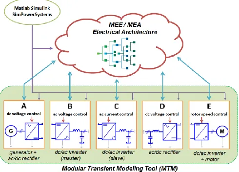
Modular Transient Modeling Tool (MTM)
[image:3.612.39.286.351.500.2]The MTM provides an alternative method to rapidly achieve stable system performance by splitting complex electrical architecture into small functional units, which individual transient response can be easily tuned and tested manually or automatically. Once the testing is complete and all units provide a stable response, they can be reconfigured back into the analysed architecture.
Tool structure
Figure 3 illustrates a system design structure, which is used to describe a MTM design methodology. In order to simplify system model development, the modelled design variants of a complex power system have been split into functional A-E subsystems. Table 1 lists examples of these subsystems.
Each A-E subsystem model is stored in a Subsystems Library and consists of interconnected replaceable modules that represent component designs and which different design options are stored in a separate Modules Library. The selection of modules is made in accordance with available components design options.
Figure 3. System design structure with MTM tool.
Once the modules have been selected and assigned to subsystem models, the transient simulation-based analysis can be performed to identify the performance of the selected modules for a particular system topology. The analysis is then repeated with a new set of modules to evaluate and compare their performance with the previous ones. In this manner, the performance of all selected components design options can be evaluated and the most promising ones identified for each subsystem model.
When necessary, the selection and allocation of the modules to subsystems for transient analysis can be automated to minimize time and provide a comprehensive identification of modules design options. The identification process can be rapidly repeated in a similar manner for other MEE/MEA system candidate architectures.
Subsystem Modeling
The internal structure of A-E subsystems from figure 4 is identical and consists of five types of modules:
Hardware Circuit – electrical circuit of sub-systems modeled with SimPowerSystems toolbox [5]. It is used to represent electrical circuitry of the subsystem components, i.e. power electronics converter, machine drives, etc. The power converters are modelled by interconnecting semiconductors and ac/dc filters.
The machines stator dynamics are modeled in dq0 rotating frame provided with electro-mechanical torque / speed interface [17]. Sensor – measures controlled instantaneous signals along with
the errors caused by A/D sampling, signal saturation, etc. Communication – signal transmission between sensor and
control circuit, which may include modelling time delays and communication errors.
Control Circuit – the algorithm used to control the operation of machine exciter or power electronics. Each subsystem has individual control command illustrated in figures 3 and 4. Modulator – the modulation method used to convert the power
electronics converter reference signal into logic binary signals associated to each single switch.
[image:4.612.39.284.247.423.2] [image:4.612.325.576.253.397.2]Table 1 lists example design options of hardware and control circuit modules associated to each subsystem. These have been selected to create a baseline MEE/MEA system model shown in figure 6.
Figure 4. Subsystems design structure with MTM tool
As figure 4 illustrates, the modules are interconnected in a closed-loop, which ensures subsystems’ full functionality. Except for a hardware circuit, all the remaining elements are built in Simulink.
[image:4.612.322.578.511.676.2]The controllable instantaneous signals current i(t), voltage v(t) and rotating speed ω(t) from the Hardware Circuit module are sent to the Control Circuit module, where they are controlled to match with the input reference values (i*, v* and ω*).
Table 1. Example design options of A-E subsystems available in MTM tool
Subsystem Design Options
Hardware Circuit Control Circuit
A Synchronous 3-phase VF generator interfaced with power electronics AC/DC rectifier
DC voltage controlled by hysteresis- band controller.
B DC bus interfaced with 3-phase power electronics DC/AC inverter
AC current controlled by rotating dq0 frame controller.
C
DC bus interfaced with 3-phase power electronics DC/AC inverter
AC current controlled by rotating dq0 frame controller.
D AC 3-phase bus interfaced with power electronics AC/DC rectifier
DC voltage controlled by hysteresis-band controller.
The controlled ac voltage reference signal v* enters the Modulator module, where it is translated into binary logic signals S* and distributed to the power electronics converter switches.
The modular design of each subsystem allows rapid replacement of any number of modules with different design options while maintaining the subsystems’ structural integrity. The module models options can be continuously updated and added to the Modules Library to incorporate novel design options.
Individual Testing and Tuning of A-E Subsystems
[image:5.612.332.569.266.685.2]A subsystem testing platform has also been created to evaluate the dynamic performance of the selected design option on an individual basis. This ensures the subsystem performs to an acceptable level prior to it being integrated into a larger and more complex power system model. Initially ’debugging’ the subsystems’ design in this way accelerates the construction of workable systems models. The execution of 1s simulation period requires 15s interval to each subsystem model.
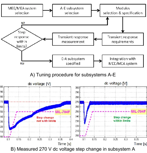
Figure 5A illustrates the tuning procedure for MTM subsystems based on example Matlab/Simulink testing of subsystem A, which is a generator-rectifier unit. The evaluation of dynamic performance is done by measuring both steady and transient response of the controlled 270 V dc voltage signal during a step change in electrical load. In this example, the imposed transient limits are obtained from MIL-704F [18]. Figure 5B demonstrates the measured load change response of the subsystem A with preliminary and optimized modules specification.
A) Tuning procedure for subsystems A-E
B) Measured 270 V dc voltage step change in subsystem A
Figure 5a): Workflow algorithm for determination of optimal A-E subsystems specification; b) dc voltage variations during transient load step change in subsystem with different specification.
The signal ripple level and transient overshoots can be compared with any limits imposed by customer, device manufacturers or power quality standards [18-19] to determine controller gains and filter size. If required, the tuning procedure can be numerically automated and optimised either via custom Matlab code or using Simulink Design Optimization™ toolbox [5] with the selected goal, e.g. minimum filtering requirements. This allows rapid evaluation of the selected
subsystems and determination of optimal parameter values. The evaluated subsystems with stable performance can be integrated into complex MEE/MEA power system model for more accurate testing.
MEE/MEA Power System Modeling
The MTM modelling strategy is presented based on a power system design illustrated in figure 6a. The selected power system architecture has been simplified to better demonstrate the modelling approach. More complex systems with multiple parallel conversion stages and machine drives (more representative of full MEE or MEA systems) can be modelled on an equivalent basis.
The modelled MEE/MEA system includes single generator unit supplying an electric pump along with dc loads and ac distribution networks operating at different frequencies. According to Table 1, subsystems A, B and E are assigned to each power conversion stage. Figure 6b presents an equivalent Matlab-Simulink electrical system which has been modelled using the MTM tool. The MTM system model includes four subsystems interconnected in parallel on a common dc busbar. The execution of 1s simulation period requires 250s interval to the complete MEE/MEA system model.
Figure 6a): Example network representation of the modeled MEE/MEA power system; b): Equivalent MTM model in Matlab/Simulink.
A)
[image:5.612.39.287.330.588.2]Assessment of the Generator-Side Rectifier
Design Options of with the MTM Tool
[image:6.612.58.260.197.371.2]Using the system illustrated in figure 6, the following sections demonstrate the use of the MTM tool to support component selection for the generator-side rectifier (marked yellow in figure 6a). Two variants are considered in this study (labelled ‘A’ and ‘B’). The selected converter topologies are presently among the most technologically mature. Variant A is a 3-level neutral point clamped (NPC) converter topology [8] with commonly used Si IGBT devices [9,20,21], while variant B is a 2-level topology [10] with less common SiC MOSFET devices [11,22,23] (SiC devices have been used due to the required voltage rating of the devices). Figure 7 presents single phase leg arrangements of each converter topology.
Figure 7.Single phase leg of active power converter: 3-level NPC [8] (left); 2-level six-switch [10] (right).
The final goal of this study is to determine how the converter made of more expensive six SiC devices with identified optimal design options can perform in comparison to the converter made of twelve conventional Si devices. The results can support the selection of the variant with more expensive SiC devices or less expensive Si devices for this particular example application.
Identification of Design Variants
The selected generator-side rectifier design variants A and B in MEE/MEA system from figure 3 are evaluated in accordance with the example design methodology presented in figure 8. In this paper study, the designs of ac/dc filters, cooling system and control circuit are kept constant to reduce number of iterations. If required, the MTM allows automated closed-loop design iterations that may include multiple revisions of the remaining component design options.
The example design methodology from figure 8 starts by defining the two core design variants of the generator-side rectifier, which are determined by the selected converter topologies: 3-level NPC converter (variant A) and 2-level converter (variant B).
In the next stage, two solid state devices are selected and assigned to each topology, thus creating four Hardware Circuit module design options. An analysis of the selected solid state switches and topologies can then take place to identify the most efficient solid state device for each topology. In this stage, a maximum device switching frequency fsw is obtained, which is later used in harmonic analysis to compare different switching techniques.
In the next stage, four Modulator module design options are considered for each generator-side topology. The resulting eight Modulator design options are evaluated against harmonic noise imposed by the switching operation of the rectifier at a frequency determined in previous stage.
Identified optimal design options with MTMST tool
Modules Selection
● Hardware Circuit
● Modulator
● Control Circuit
● Communication
● Sensors
Hardware Circuit (Solid State Switches)
Design Options Variant A Variant B
● SiC ROHM BSM300D
● SiC CREE CAS300M
● Si INFINEON FL300R ● Si SEMIKRON SKiM301ML
Modulator
● Triangular PWM
● Sawtooth PWM
● Inverse sawtooth PWM ● Phase-shifted triangular PWM ● Level-shifted triangular PWM ● Inverse level-shifted triangular PWM ● Space Vector Modulation SVM
Component (Generator-Side Rectifier)
Power Losses Analysis
MTM System Model
Design Options Variant A Variant B
2. Selection of analyzed modules design options
Hardware Circuit (Converter Topology)
Design Options Variant A Variant B ● 3-level NPC ● 2-level (six-switch)
Harmonic Analysis
Fault Analysis
Subsystems Selection
●Subsystem A
●Subsystem B
●Subsystem C
●Subsystem D
●Subsystem E
MEE/MEA Architecture Candidate
MTMST Rectifier Variants A and B
1. Selection of analyzed components & modules
3. Selection of subsystems &
MEE/MEA network modelling 4. Identification of optimal design options Identified min. filter size LAC
Identified max. switching frequency fsw
[image:6.612.42.573.410.690.2]
Harmonic analysis allows identification of optimal modulation techniques for each topology. The modulation methods are compared with regard to ac load current Total Harmonic Distortion (THD) factor [19]. During this stage, minimum ac/dc filtering requirements are determined to maintain current harmonics below limits specified in RTCA DO-160F [19]. The estimated ac/dc filter parameter values are used in a fault analysis to accurately characterize temperature rise during faults.
Finally, the level of fault tolerance of the rectifier variants A and B is evaluated during short circuit faults. The dynamic electro-thermal models of the solid-state switches are used to identify maximum fault periods, during which the junction temperature does not exceed permissible thresholds. The results can support the design of optimal fault protection scheme and fault management strategies.
Solid State Devices
The emerging SiC MOSFET power modules [11] are a promising technology and offer a number of attractive characteristics when compared to commonly used silicon. In particular, the much higher breakdown field strength and thermal conductivity of SiC allow switching at much higher frequencies and convert electric power with lower losses. Additionally, SiC-based devices manage the same level of power as Si devices at half the size, thus leading to increased power density.
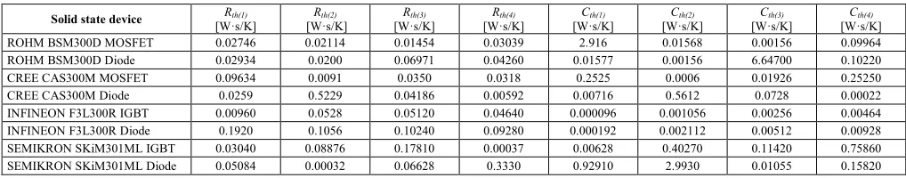
Presently available SiC MOSFET modules are relatively expensive and start their voltage ratings from 1200 V. In +/- 270V dc distribution systems, this makes their utilization more effective for 2-level converter topologies rather than the 3-2-level NPC from figure 4. On the other hand, Si IGBT devices [9] are available in wide range of voltage ratings and they are approximately 3 times lower in price than the equivalent SiC devices [24]. As a result, they can be readily used in 3-level converter topologies to minimise harmonic distortions [8]. Table 2 lists the selected devices with key parameter values, which have been used to determine maximum switching frequencies, power losses and maximum fault periods. The switching and thermal curves are provided in device datasheets [20-23].
Dynamic Electro-Thermal Modeling
The MTM allows investigations into the thermal impact of system operation on semiconductors. This is achieved using integrated dynamic junction temperature and power loss estimation models. These models can measure and register transient junction temperature and power loss variations of each individual semiconductor during normal and fault conditions.
The developed electro-thermal model calculates the transient temperature change based on estimated instantaneous power losses from the instantaneous output current i(t), voltage v(t), temperature Tj(t) and datasheet parameters in Table 1.
Figure 9 illustrates the top-level flow chart of the developed device electro-thermal model. This proposed power loss modelling
approach is consistent with that presented in [25-27], which is a commonly accepted method for loss evaluation of power semiconductor devices.
Figure 9. Top-level flow chart used to estimate power losses and junction temperatures
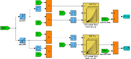
The Matlab/Simulink implementation of a MTM device loss model [28] is shown in figure 10. Three-dimensional look-up tables are used to determine the dissipated energy values based on the device characterization in manufacturer datasheets. Loss models of the diodes are of similar design. However, they do not include forward recovery losses generated during the turn-on, which are considered negligible and normally neglected for switching frequencies below 400 kHz [29].
Figure 10. Matlab/Simulink model for semiconductors switching loss calculation
During normal operation, the electro-thermal model can be used to estimate power losses and junction temperature levels. During abnormal operation, the thermal model of a single device is capable of indicating the junction temperature rate of rise, for example when the device is subjected to excessive fault current. Figure 11 illustrates the developed model, in which the thermal impedance from junction to ambient Zth(j-c) is modelled as a six-layer Foster RC network [25-27]. Such a network allows accurate estimation of the temperature rise between junction and ambient.
The thermal resistance Rth will determine the steady state value of junction temperature and the thermal time constant τRC. The τRC can be calculated from
[image:7.612.327.576.82.150.2]τRC = Rth · Cth. (1) This will dictate the dynamic change of the junction temperature Tj.
Table 2. Evaluated solid state switch design options against power losses and post-fault behavior [20-23]
Device specification Device type voltage [V] Nominal current [A] Nominal Turn-on time t
on [ns]
Turn-off time toff [ns]
Junction temp. Tj(nom)
[0C]
Thermal resistance junction-case Rth(j-c)
[K/W]
Stray inductance Ls
[nH]
ROHM BSM300D12P2E001 SiC MOSFET Module 1200 300 150 315 150 0.035 1) 0.035 2) 13
CREE CAS300M12BM2 SiC MOSFET Module 1200 300 144 211 150 0.035 1) 0.035 2) 14
INFINEON F3L300R07PE4 Si IGBT Module 600 300 180 590 150 0.0631) 0.125 2) 45
SEMIKRON SKiM301MLI07E4 Si IGBT Module 600 300 230 600 150 0.0631) 0.125 2) 22
[image:7.612.324.577.273.388.2] [image:7.612.36.575.604.703.2]The values for thermal capacitance Cth can be obtained by extrapolating thermal curve characteristics provided by device manufacturers [20-23].
Figure 11a): Thermal circuit model of semiconductor power module used for junction temperature estimation; b) Transient thermal impedance RC Foster network representation
During the steady state and fault period, the inlet coolant temperature TCW is assumed constant due to the fault’s relatively short duration. The RC parameter values of semiconductor junction-case transient thermal impedance Zth(j-c) can either be found directly from the manufacturers' datasheets, or approximated by a curve fitting tool (e.g. cftool in Matlab [5]). The case-sink thermal resistance Rth(c-s) values are listed in Table 2.
The thermal resistance value of the selected cooling systems cold plate Rth(s-CW) is obtained directly from manufacturers' datasheet [30]. This has been specified in Table 3, where the selected tube liquid cold plate is identical in each analyzed design option.
The thermal capacitance can be approximated from
s s CW s
th m c
C ( ) , (2)
[image:8.612.46.279.76.521.2]where ms is mass and cs is the specific heat of the selected cold plate material from Table 3.
Table 3. Cooling system cold plate specification [30].
Manufacturer Aavid Thermalloy
Model no. Tube liquid 418101U00000G
Coolant's flow rate F [l/min] 10
Thermal resistance Cth(s-CW) [K/W] 0.015
Cold plate material Aluminum
Mass ms [kg] 1.34
Specific heat cs [kJ / kg·K] 0.91
Thermal capacitance Cth(s-CW) [kW·s / K] 1.22
The transient temperature rate of change Tj(t) is estimated from
() ()
6
1 ) ( 1
) ( )
( tRthi Cthi
i i th d
j t P t R e
T
(3)with the total dissipated power Pd(t) made by switching and conduction losses. Table 7 in Appendix lists Rth(i) and Cth(i) input values from semiconductor device manufacturer datasheets used to model the transient junction temperature variations.
Junction Temperature Variations during Normal Operation
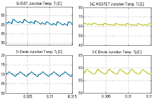
[image:8.612.327.577.452.618.2]Figure 12 illustrates an example, where the registered junction temperature variations Tj of the SiC MOSFET modules are compared with the variations of Si IGBT modules during normal operation at identical switching frequency. This figure clearly demonstrates the superior thermal performance of SiC devices over the silicon, where the actual registered device junction temperature of the diodes and switches is increased nearly by half.
Figure 12. Example simulated junction temperature variations during normal operation in silicon (left) and silicon-carbide (right) power modules.
As a result, the switching frequency of converter with SiC components can be significantly increased to minimize harmonic distortions and filtering requirements with no impact on cooling system design.
A)
Junction Temperature Variations during Fault Operation
The developed MTM dynamic electro-thermal model for solid state devices can be used not only for rapid sizing of the converter or comparing devices from different vendors. It can be also used to characterize the device dynamic thermal behaviour under fault conditions. This enables the evaluation of fault tolerant operation or specification of overload and fault protection systems.
[image:9.612.325.573.60.174.2]Figure 13 illustrates examples of the transient junction temperature rise of the semiconductor power modules due to ac short-circuit fault across the 360-800 Hz section of network from figure 3.
Figure 13. Example junction temperature variations during fault operation in silicon (left) and silicon-carbide (right) power modules.
When the actual temperature exceeds the permissible limit in the MOSFET or IGBT, the device needs to be instantly turned off to avoid thermal damage [31]. However, anti-parallel diodes cannot be turned off and a separate protection system, capable of isolating the diodes in case the actual junction temperature exceeds permissible limits, may be required.
The simulation graphs demonstrate that in this case the ac short-circuit fault leads to the excessive junction temperatures across IGBTs and MOSFETs, while the temperatures of anti-parallel diodes remain within the safe limits.
The required minimum blocking period is 15ms for the converter with Si IGBTs and around 1ms for the equivalent converter with SiC MOSFETs. This means that the system with SiC components can be re-energized almost 15 times faster in comparison to the equivalent silicon-based converter.
Modulation Techniques
The sinusoidal vABC* reference signal from figure 4 needs to be converted to binary logic state signals of the solid state switches. The conversion can be performed in many ways, which may differ in signal distortion levels [32-35]. As a result, identification of optimal modulation methods can be used to reduce filtering requirements and increase overall power density.
This paper compares four applicable modulation techniques applicable for each of the 2-level and 3-level converter topologies in variants A and B. The comparison is used to determine an optimal switching combination, which results in the lowest phase current harmonic distortions.
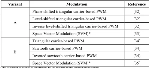
The examined modulation techniques have been listed in Table 4. Each modulation technique corresponds to the modulator design option from figure 8. The developed modulator options are stored in MTM library and can be re-used whenever necessary for different case studies.
[image:9.612.36.287.156.317.2]Table 4. Evaluated modulation techniques for rectifier variants A and B [32-35].
Variant Modulation Reference
A
Phase-shifted triangular carrier-based PWM [32] Level-shifted triangular carrier-based PWM [32] Inverse level-shifted triangular carrier-based PWM [32]
Space Vector Modulation (SVM)* [33]
B
Triangular carrier-based PWM [34]
Sawtooth carrier-based PWM [34]
Inverted sawtooth carrier-based PWM [34]
Space Vector Modulation (SVM)* [35]
* The switching sequence is determined by the position of the nearest three vectors
Power Quality Studies
Power quality studies can also be carried out using the MTM. This allows a comparison of the harmonic output for different design options. Figure 14 illustrates the example simulation results of an ac phase current harmonics in a power system from figure 4. The results are generated for 400 Hz generator frequency under 100% loading. The obtained current harmonic levels are compared with power quality requirements from RTCA DO-160F [19].
A) Harmonic analysis of variant A (fsw = 30 kHz)
b)
[image:9.612.323.581.291.559.2]B) Harmonic analysis of variant B (fsw = 30 kHz)
Figure 14. Harmonic frequency spectrum of ac phase current compared with RTCA DO-160F limits in a): 3-level rectifier; b) 2-level rectifier.
The figure illustrates different phase current harmonic spectra for each converter topology switched at fsw = 30 kHz. The results are visualized for triangular and phase-shifted PWM design options. During measurements, the VF generator rotates at 400 Hz.
Total Harmonic Distortion (THDi)
The calculated current Total Harmonic Distortion (THD) factor from
1 40
2 2
100
I
I
THD
nn
i
(4)is used as a single merit to quantitatively evaluate the performance of all eight considered modulator design options.
The calculated THDi represents the ratio of the sum of the measured ac loads rms currents In of all harmonic components to load rms current I1 of the fundamental frequency [16].
Simulation Results
This section presents results which compare the generator-side rectifier design options for MEE/MEA system in figure 6. The MEE/MEA system model has been developed with MTM tool in Matlab/Simulink based on specification from Table 7 in Appendix.
The component selection from figure 8 has been divided into three parts: power losses analysis, harmonic analysis and fault analysis. In the first part, the selected design options for solid state switches from figure 8 and specified in Table 2 have been evaluated against generated power losses over a 360-800 Hz frequency range. For each rectifier design variants A and B, the devices’ maximum allowable switching frequency is determined, which allows continuous operation within thermal limits for the fixed cooling system design from Table 2.
In the second part, the modulation techniques are compared for the previously determined set of switching frequencies. The comparison is performed by calculating THD from measured ac loads phase current harmonics. In a similar manner to power losses analysis, MEE/MEA system simulations are made over a 360-800 Hz frequency range for a comprehensive evaluation.
Final part demonstrates the post-fault behaviour of the selected solid state switches with the previously determined maximum switching frequency and modulator design option. Short circuit faults are simulated to determine the maximum allowed fault period for uninterrupted operation. Finally, the rectifier blocking period caused by overheating is compared, during which the converter remains functionally blocked and cannot supply power to the DC-side (regardless of the fault period).
Power Losses Analysis
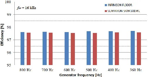
The estimated efficiency levels of the generator-side rectifier designed in accordance with variants A and B have been illustrated in figures 15 and 16. The efficiency is estimated over a 360-800 Hz range at 100% load.
The determined maximum switching frequency fsw(A) for variant A (the 3-level NPC equipped with Si IGBTs) is 16 kHz. This is limited by the thermal capability of the SEMIKRON SKiM301ML (Tj(nom) = 1500C). The INFINEON FL300R heats up to 1300C, thus allowing switching at fsw = 24 kHz.
[image:10.612.324.576.40.172.2]Power losses between analyzed Si IGBTs in variant A are relatively similar, with overall efficiency levels of 97.7% for INFINEON FL300R and 97.6% for SEMIKRON SKiM301ML.
Figure 15. Estimated efficiency levels in variant A rectifier for different solid state switch design options.
In variant B with 2-level converter equipped with SiC MOSFETs, the determined maximum switching frequency is 38 kHz, which is almost 2.5 times higher than in variant A. The maximum switching frequency is limited at Tj(nom) = 1500C by ROHM BSM300D. At this frequency, the CREE CAS300M heats only up to Tj = 1100C, which allows switching at increased frequency up to fsw = 50 kHz.
[image:10.612.325.576.318.436.2]According to figure 16, the highest power losses are associated with ROHM BSM300D, resulting in a rectifier efficiency of approx. 96.5%. On the other hand, the rectifier with CREE CAS300M generates the lowest losses, leading to overall 98% efficiency.
Figure 16. Estimated efficiency levels in variant B rectifier for different solid state switch design options.
The simulation results show that the MTM tool can not only compare the efficiency of different converter topologies but can also take account of characteristic variance at the device level.
Harmonic Analysis
The THD levels of 3-phase currents flowing through ac-side loads are compared against each described modulation technique for variants A and B. Figures 17 and 18 illustrate the obtained THD values, with variant A switched at fsw(A) = 16 kHz, and variant B switched at fsw(B) = 38 kHz. The distortion levels have been measured at 100% load.
In variant A, the lowest THD of 2.94% is provided both by phase-shifted triangular carrier-based PWM and by SVM-NTV technique. The highest distortion level of 4.04% is generated at 800 Hz in level-shifted triangular carrier-based PWM.
inverse sawtooth PWM technique at VF generator operating at 500 Hz.
Figure 17. Estimated ac current THD levels in variant A rectifier for different modulator design options.
[image:11.612.39.287.65.188.2]The harmonic analysis clearly demonstrates that SVM-NTV technique in variants A and B results in very good quality phase current waveforms, and therefore it can be considered as the preferred design option (from the technologies considered) for the generator-side rectifier in MEE/MEA power system from figure 18.
Figure 18. Estimated ac current THD levels in variant B rectifier for different modulator design options.
Fault Analysis
The analysis investigates the impact of short circuit system faults on the converter performance. The simulation results presented relate only to ac side faults, which can be used to evaluate fault tolerant capability of the converter. In case of dc side short circuit faults, the converter is unable to supply any power. However, thermal withstand of semiconductor components needs to be evaluated to ensure that converter is able to sustain any fault current contribution. During dc short circuit analysis with the ac/dc filter parameters determined previously, it was found that the diodes operating at steady junction temperatures do not exceed temperature limits (Tj(max) = 1500C from Table 2). As a result, they are able to withstand the flow of excessive fault currents from the generator.
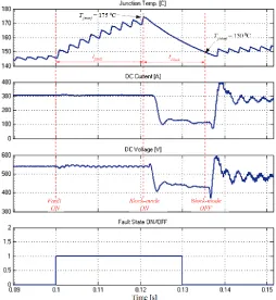
Figure 19 illustrates the effect of a simulated phase-ground short circuit fault on the analyzed variant A rectifier and dc network.
Due to the fault, the ac line voltage on the faulted phase collapses, which results in voltage drop across the dc distribution bus.
This causes the rectifier Control Circuit module to command higher currents to flow through the switches in healthy phases in order to maintain constant dc voltage across the +/- 270 V distribution system.
Figure 19. Generator-side variant A rectifier post-fault behavior during ac short-circuit faults (phase-shifted triangular PWM; INFINEON FL300R).
The increased currents flowing through the semiconductor switches result in their junction temperature rise. If the fault is not cleared fast enough by the protection system, the junction temperature may exceed maximum limits Tj(t) > 1750C and lead to activation of the converter block-mode, where all semiconductor switches are turned off and the converter is temporarily out of service [31]. Until the junction temperature of the solid state switches drops down to safe level Tj(t) 1500C, the rectifier cannot provide the required amount of power to the dc distribution system.
Table 5 presents measured fault periods tfault when junction temperature rises above 1750C and the duration of the rectifier blocking period tblock for each analyzed set of solid state switches. The results can be used to support the selection of fault protection units in order to maintain uninterruptible power supply to dc distribution system or to determine the time for fault recovery of the rectifier in variants A and B. The obtained values vary significantly with regard to the type of semiconductor. Analyzed SiC devices tend to both heat up and cool down much faster than the presently utilized silicon-based IGBTs.
Table 5. Simulation results of fault-tolerant and recovery periods of the rectifier with different topology and solid state switch design variants.
Solid State
Device Min. fault-tolerant period t[ms] fault Max. blocking period tblock [ms]
INFINEON
FL300R 21.1 15.21
SEMIKRON
SKiM301ML 18.7 24.34
ROHM
BSM300D 0.363 2.203
CREE
CAS300M 0.401 6.129
[image:11.612.38.288.282.405.2] [image:11.612.323.577.570.678.2]kHz result in rapid overheating of variant B rectifier within the first millisecond of fault occurrence. As a result, a fast-acting protection unit is required that clears the fault before 400 μs in order to maintain fault-tolerant capability of the SiC rectifier. Variant A with Si IGBTs switched at fsw = 16 kHz have longer transient thermal time constants that allow them to continuously operate 15 ms after the fault occurrence.
The maximum registered blocking period of SiC devices is approx. 6 ms. Once the blocked-mode is activated, the variant B rectifier is able to recover 3 times faster than variant A unit. This demonstrates that variant A rectifier has higher fault tolerant capability, while variant B has higher capability for fault recovery. The priority and importance of each feature needs to be examined in detail against individual requirements of the selected electrical loads in MEE/MEA power system.
Summary
The identification and selection of optimal design options is of major importance for MEE/MEA electrical systems planning and development. Today, wide range of existing technology solutions and components available on the market makes the benchmarking practice both challenging and time-absorbing.
Existing simulation-based modelling tools can minimize cost efforts on MEE/MEA system development by comparing the design options at early stage. However, high modelling skills are normally required and significant amount of time needs to be allocated to perform a comprehensive analysis with multiple design options.
This paper presents a MTM tool, which can be used to accelerate and simplify determination of the most promising systems and components designs by rapid and simple modelling of complex electrical architectures. The tool has been developed in Matlab/Simulink and consists of two libraries. The first Subsystems Library is used to construct and evaluate MEE/MEA transient circuit models made from functional subsystems. The second Modules Library is compatible with SimPowerSystems library and can be used to assign specific design options in a plug and play manner to each subsystem that represents power electronic converters or machine drives.
If multiple combinations and configurations of design options need to be evaluated, the MTM can be automated to minimize time between iteration cycles. In the automated mode, the pre-selected design options and MEE/MEA architecture candidate are automatically evaluated either against an agreed set of requirements or against the formulated objective function. This makes the MTM suitable for behavioral level analysis to support various engineering studies in actual MEE/MEA system design.
The performance of the MTM is further demonstrated on the example MEE/MEA network, where two different design variants of the generator-side rectifier are considered. Each variant consists of six design options: two for rectifier solid state switches and four for the modulation method.
The MTM is used both to evaluate the selected rectifier hardware components and switching control algorithms against three criteria: power losses, power quality and fault tolerance. For each variant, simulation results have identified optimal set of solid state switches and modulation strategy. Finally, design considerations have been identified for ac fault protection unit and dc-side loads, which may impact their reliable operation. This corresponds to the required maximum fault clearing time of the protection and minimum fault recovery period of the rectifier.
References
1. Bhangu, B., Rajashekara, K., “Electric Starter Generators: Their Integration into Gas Turbine Engines,” IEEE Industry Applications Magazine 20(2): 14-22, 2014, doi: 10.1109/MIAS.2013.2288398.
2. Oyori, H., Nakagawa, S., Saito, H., Takahashi, N. et al., "System Concept Study of Electrical Management for Onboard Systems," SAE Technical Paper 2014-01-2200, 2014, doi:10.4271/2014-01-2200.
3. Purellku, I., Lucken, A., Brombach, J., Nya, B., et al., “Optimization of the Energy-Supply-Structure of Modern Aircraft by Using Conventional Power System Technologies,” CIRED 2011, No. 0973, Germany, 2011.
4. Moir, I., Seabridge, A., “Aircraft Systems: Mechanical, Electrical and Avionics Subsystems Integration,” (Aerospace Series, Wiley, 2008), pp 182, ISBN: 0470770945.
5. Moler, C., MATLAB (Version R2014a), Computer Software, MathWorks Inc., Massachusetts, 2014.
6. Amrhein, M., Wells, J., Walters, E., McNeal, S. et al., "Impact of Transient Operating Conditions on Electrical Power System and Component Reliability," SAE Int. J. Aerosp. 7(1):99-108, 2014, doi:10.4271/2014-01-2144.
7. Nanawi, A., Fong, C., Liu, Y., Sakanova, A., et al., “Design of high power density converter for aircraft applications,” presented at ESARS 2015, Germany, March 3-5, 2013-5, doi: 10.1109/ESARS.2015.7101418.
8. Santos, E., Silva, E., “Advanced Power Electronics Converters: PWM Converters Processing AC Voltages, ” (Wiley-IEEE Press, 2015), 88-124, ISBN: 978-1-118-88094-4
9. Perret, R., “Power Electronics Semiconductor Devices,” (ISTE Ltd and John Wiley & Sons, Inc., 2009), 57-74, ISBN: 978-1-84821-064-6
10. Santos, E., Silva, E., “Advanced Power Electronics Converters: PWM Converters Processing AC Voltages, ” (Wiley-IEEE Press, 2015), 25-50, ISBN: 978-1-118-88094-4
11. Nakamura, T., Sasagawa, M., Nakano, Y., Otsuka, T. and Miura, M., “Large current SiC power devices for automobile applications,” presented at IPEC 2010, Japan, June 21-24, 2010.
12. Muller-Glaser, K., “Model-Driven Engineering for Automotive Systems,” Panel Presentation at SAASE 2009 Symposium on Automotive/Avionics Systems Engineering, Oct. 2009.
13. Kuhn, M., Otter, M., and Raulin, L., “A Multi Level Approach for Aircraft Electrical Systems Design,” presented at Modelica’2008., Germany, March 3-4, 2008.
14. Mollov, S., Forsyth, A., and Bailey, M., "System Modeling of Advanced Electric Power Distribution Architectures for Large Aircraft," SAE Technical Paper 2000-01-3631, 2000, doi:10.4271/2000-01-3631.
15. Bengtsson, M., and Isaksson, D., “Modelling a Distributed Power System in Saber®,” MSc thesis, Department of Environment and Energy, Chalmers University of Technology, Goteborg, 2008.
16. Li, X., Kher, S., Huang, S., Ambalavanar, V., and Hu, Y., “System Level Component Modeling of Aircraft Electrical System Using VHDL-AMS,” WCECS 2015, USA, October 21-23, 2015.
17. Abu-Rub, H., Iqbal, A., and Guzinski, J., “High Performance Control of AC Drives with Matlab / Simulink Models,” (John Wiley & Sons, 2012), 19-42, ISBN: 978-0-470-97829-0.
18. Department of Defense Interface Standard, "Aircraft Electric Power Characteristics," MIL Standard 704F, Rev. Oct. 2013.
19. Radio Technical Commission for Aeronautics (RTCA), “DO-160, Environmental Conditions and Test Procedures for Airborne Equipment,” RTCA Standard DO-160F, Rev. Dec. 2007.
20. Si Power Module 600 V / 300 A INFINEON F3L300R07PE4, Datasheet,
http://infineon.com/, accessed Mar. 2016.
21. Si Power Module 600 V / 300 A SEMIKRON SKiM301MLI07E4, Datasheet,
http://semikron.com/, accessed Mar. 2016.
22. SiC Power Module 1200 V / 300 A ROHM BSM300D12P2E001, Datasheet,
http://rohm.com/, accessed Mar. 2016.
23. SiC Power Module 1200 V / 300 A CREE CAS300M12BM2, Datasheet,
http://cree.com/, accessed Mar. 2016.
24. Digi-Key Electronics, Electronic Components Distributor, USA,
http://digikey.com, accessed Mar. 2016.
25. User manual of PLECS blockset version 3.1, March 2011,
http://plexim.com/files/plecsmanual.pdf, accessed Mar. 2016.
26. Stupar, A., Bortis, D., Drofenik, U., and Kolar, J., “Advanced setup for thermal cycling of power modules following definable junction temperature profiles,” presented at IPEC 2010, Japan, June 21-24, 2010, doi: 10.1109/IPEC.2010.5542179.
28. Ivakhno, V., Zamaruiev, V., and Ilina, O., “Estimation of Semiconductor Switching Losses under Hard Switching using Matlab/Simulink Subsystem,” Electrical, Control and Communication Engineering 2(1):20-26, 2013, doi: 10.2478/ecce-2013-0003.
29. Jordan, J., Magraner, J., Cases, C., Esteve, V., et al. “Turn on switching losses analysis for Si and SiC diodes in induction heating inverters,” presented at EPE 2009, Spain, September 8-10, 2009.
30. Tube Liquid Cold Plate, Aavid Thermalloy 418101U00000G, Datasheet,
https://aavid.com, accessed Mar. 2016.
31. Wang, K., Liao, Y., Song, G., Ma, X., “Over-Temperature protection for IGBT modules,” presented at PCIM 2014, Germany, May 20-22, 2014.
32. Holmes, D., and Lipo, D., “Pulse Width Modulation for Power Converters: Principles and Practice,” (John Wiley & Sons, 2003), 453-531, ISBN: 047-1-208-140.
33. Wu, B., “High-Power Converters and AC Drives,” (John Wiley & Sons, 2006), 101-115, ISBN: 10 0-471-73171-4.
34. Wilamowski, M., and Irwin, J., “Power Electronics and Motor Drives,” (CRC Press, 2011), 14/27-14/36, ISBN: 978-1-4398-0286-1
35. Neacsu, D., “Switching Power Converters: Medium and High Power,” (CRC Press, 2014), 485-499, ISBN: 978-1-4665-9193-6.
Acknowledgments
This work has been carried out as part of the Rolls-Royce UTC program.
Definitions/Abbreviations
A/D Analog-digital
IGBT Integrated gate bipolar transistor
MEE/MEA Electric Engine /
More-Electric Aircraft
MOSFET Metal-oxide semiconductor
field-effect transistor
MTM Modular transient modelling tool
NPC Neutral point clamped
PWM Pulse width modulation
Si Silicon
SiC Silicon carbide
SVM Space vector modulation
THD Total harmonic distortion
VF Variable frequency
[image:13.612.49.563.366.533.2]Appendix
Table 6. Specification of MEE/MEA system model used in simulation studies.
Subsystem Component Parameter Value Subsystem Component Parameter Value
Subsystem A
VF synchronous generator
Rated power [kVA] 215
Subsystem E
PMSM motor
Rated power [kVA] 10
Rated voltage [V] 230/400 Rated voltage [V] 115/200
Rated frequency [Hz] 360-800 Rated speed [RPM] 17000
Stator winding resistance [Ω] 1·10-3 Stator winding resistance [Ω] 2·10-3
The d-axis inductance [H] 1.85·10-4 The d-axis inductance [H] 2.83·10-4
The q-axis inductance [H] 1.66·10-4 The q-axis inductance [H] 2.87·10-4
Pole pairs [-] 4 Pole pairs [-] 5
Generator-side rectifier
A/D sampling frequency [kHz] 100 Voltage constant [V/kRPM] 24
Switching frequency [kHz] 16 / 38
Motor-side inverter
A/D sampling frequency [kHz] 100
dc filter capacitance [F] 1·10-3 Switching frequency [kHz] 20
ac filter inductance [H] 2·10-4 dc filter capacitance [F] 1·10-3
Subsystem B
ac network
Rated power [kW] 18
Subsystem B
ac network
Rated power [kW] 5
Rated voltage [V] 115/200 Rated voltage [V] 115/200
Rated frequency [Hz] 400 Rated frequency [Hz] 50
Power electronics inverter
A/D sampling frequency [kHz] 100
Power electronics inverter
A/D sampling frequency [kHz] 100
Switching frequency [kHz] 20 Switching frequency [kHz] 20
dc filter capacitance [F] 1·10-3 dc filter capacitance [F] 1·10-3
ac filter inductance [H] 1.5·10-4 ac filter inductance [H] 9·10-4
Table 7. Extrapolated transient thermal impedance factors from the thermal curve characteristics used to create RC Foster network models [25-27]
Solid state device Rth(1)
[W·s/K] [W·s/K] Rth(2) [W·s/K] Rth(3) [W·s/K] Rth(4) [W·s/K] Cth(1) [W·s/K] Cth(2) [W·s/K]Cth(3) [W·s/K]Cth(4)
ROHM BSM300D MOSFET 0.02746 0.02114 0.01454 0.03039 2.916 0.01568 0.00156 0.09964
ROHM BSM300D Diode 0.02934 0.0200 0.06971 0.04260 0.01577 0.00156 6.64700 0.10220
CREE CAS300M MOSFET 0.09634 0.0091 0.0350 0.0318 0.2525 0.0006 0.01926 0.25250
CREE CAS300M Diode 0.0259 0.5229 0.04186 0.00592 0.00716 0.5612 0.0728 0.00022
INFINEON F3L300R IGBT 0.00960 0.0528 0.05120 0.04640 0.000096 0.001056 0.00256 0.00464
INFINEON F3L300R Diode 0.1920 0.1056 0.10240 0.09280 0.000192 0.002112 0.00512 0.00928
SEMIKRON SKiM301ML IGBT 0.03040 0.08876 0.17810 0.00037 0.00628 0.40270 0.11420 0.75860
[image:13.612.51.560.553.653.2]![Figure 1. Multi-stage design process of systems and components [12]](https://thumb-us.123doks.com/thumbv2/123dok_us/1561434.108758/3.612.326.577.202.373/figure-multi-stage-design-process-systems-components.webp)
![Figure 7.Single phase leg of active power converter: 3-level NPC [8] (left); 2-level six-switch [10] (right)](https://thumb-us.123doks.com/thumbv2/123dok_us/1561434.108758/6.612.42.573.410.690/figure-single-phase-active-power-converter-level-switch.webp)