Abstract— A strong candidate device for use in high-efficiency and high-density power converters is the SiC BJT, which requires a continuous gate (base) current to maintain its ON-state. A base driver circuit with regenerative collector current feedback using a current transformer, and a negative off-state base-emitter voltage is presented in this paper. The off-state base-emitter voltage required to prevent simultaneous conduction of a commercially available device when subjected to dv/dt’s is assessed. The device is then utilized in a three-phase DC to AC power converter where the efficacy of using the proposed base driver is evaluated. The off-state base-emitter voltage used is informed by the dv/dt tests. The converter is supplied from a 600-V DC rail, switches at 50 kHz and supplies a 4.1-kW load at a modulation index of 0.9. An efficiency of 97.4% was measured.
Index Terms—Base driver, dv/dt, power converter, SiC BJT, simultaneous conduction.
I. INTRODUCTION
ide bandgap devices [1], [2], offer performance benefits when compared to their silicon counterparts, and candidate devices for use in high-efficiency power converters are SiC MOSFETs and bipolar junction transistors (BJTs). The SiC MOSFET exhibits low switching and conduction losses and has been evaluated in applications such as those in [3] and [4]. However, challenges include gate oxide reliability [5], and susceptibility to dv/dt-induced conduction (“crosstalk”) [6], [7], in voltage source converters (VSCs). It is difficult avoiding crosstalk whilst not exceeding the maximum allowed off-state gate-source voltage of typically -10 V. Furthermore, compared to the silicon MOSFET, they tend to exhibit a low ratio of absolute maximum to threshold gate voltage. This presents the challenge of rapidly driving the gate to attain low switching losses at turn-on, yet also ensuring that gate-source
over-voltage transients exceeding the absolute maximum value are avoided [8].
Like the SiC MOSFET, the SiC BJT exhibits low switching and conduction losses, good short-circuit withstand times and absence of second breakdown [9]-[17]. In addition, the SiC BJT’s base-emitter junction is formed from an inherently robust pn diode structure, it has no oxide layer and can operate at higher temperatures than the SiC MOSFET. A feature of the SiC BJT is that it does not require a carefully controlled voltage applied to its control (base and emitter) terminals in the on-state because it presents a forward biased pn diode junction. It can also withstand a high reverse control voltage in the off-state. However, unlike MOS-gated devices, it needs a steady-state base current iB to hold it on as well as transient base currents for
rapid switching. The SiC BJT can simply be supplied with the
iB needed to cater for the highest collector current iC that will be
encountered. However, this introduces inefficiency when supplied at lower iC values, and making iB proportional to iC is
therefore desirable.
In [16] the problem of power dissipation in the driver circuit due to sourcing iB is addressed by using a low-voltage base
driver supply rail to supply the steady ON-state iB in
conjunction with a higher voltage rail for supplying the high transient current needed for rapid turn-on. However, iB is still
fixed for the worst-case iC with consequent losses in the driver
circuit and the SiC BJT, and an additional base driver power supply rail is needed.
Proportional drive schemes for the SiC BJT are proposed in [18]-[20]. Dissipative arrangements are used in [18] and [19]. In [18], the choke current in a boost converter using a SiC BJT is sensed with a Hall-effect sensor. In response to this sensed current, iB is set at one of a number of discrete levels by a DSP
which controls a combination of switches which source currents into the base of the BJT. In [19] the choke current in a boost converter is also sensed with a Hall-effect sensor and the sensor’s output signal is applied to the gate of a silicon MOSFET which regulates the flow of iB into a SiC BJT’s base.
In [20], a current transformer (CT) is used in a proportional driver circuit for a SiC BJT. Apart from providing a proportional base current, another advantage of using a CT is that it is ideally lossless as the current is not sourced through a dissipative element from a voltage supply. In practice there are
Evaluation of the Off-State Base-Emitter
Voltage Requirement of the SiC BJT with a
Regenerative Proportional Base Driver Circuit
and their Application in an Inverter
Neville McNeill, Bosen Jin, Xibo Yuan,
Senior Member, IEEE
, and Ian Laird,
Member, IEEE
W
This work was partly supported by the EPSRC National Centre for Power Electronics under grant EP/R004137/1 and EP/K035096/1. N. McNeill is with the Department of Electronic and Electrical Engineering, University of Strathclyde, Glasgow, G1 1XQ, U.K. (e-mail: neville.mcneill@strath.ac.uk).
some losses due to factors such as CT core losses and the forward voltage drop of the rectifier diode normally required in series with the CT’s secondary winding. The current gain of the SiC BJT is inversely related to its temperature and the current transfer ratio of the CT cannot be changed to accommodate this. This ratio, which is essentially dependent on the turns-ratio, therefore has to be set for the worst-case (highest) temperature that might be encountered. However, in many practical applications there is little variation in the device operating temperature of the SiC BJT [18] and there is consequently little excess power dissipation incurred in the driver circuit or device by driving the BJT with an excessive iB at low temperatures.
There is work on proportional drive schemes with CTs for earlier silicon BJTs in [21] and [22]. However, ensuring operation at high duty cycles is more challenging at the higher switching frequencies used with the SiC BJT.
This paper proposes a regenerative proportional base driver with a negative off-state voltage for the SiC BJT where CT is used to drive the BJT’s base with a fraction of its collector current. The dv/dt-induced conduction characteristic of the BJT is evaluated for different conditions of rail voltage, temperature and off-state base-emitter voltage. Whilst much literature is available on the SiC MOSFET’s negative off-state gate-source requirement, and other mitigating measures [23] to address simultaneous conduction, the off-state requirements of the BJT have not been investigated in as much detail. Minimizing the displacement charge drawn through dv/dt-induced conduction is important as, otherwise, increased power dissipation and reduced efficiency results. Finally, the efficacy of the driver is demonstrated in an inverter. Unlike most DC-DC power converters, operation with duty cycles approaching 100% is normally desirable in an inverter. Where a CT is used, this presents the challenge of attaining high duty cycle operation by ensuring that the CT core flux is reset during short off-times.
This paper is organized as follows. Section II describes the CT operation with regenerative collector current feedback and presents a base driver circuit. The circuitry in Section II has been presented in [24], and an extended description is given here. A comparison of the CT core flux resetting method in [24] with conventional resetting using a discrete clamping circuit is made. The maximum duty cycle limitations of the scheme in [24] are described in further detail. Section III contains an experimental evaluation of the negative off-state base-emitter voltage requirement of a SiC BJT. Section IV presents an evaluation of the performance of the BJT with regenerative base driver circuitry using a CT in a three-phase inverter application. A discussion is included in Section V.
II. BASE DRIVER OPERATION WITH REGENERATIVE CURRENT
FEEDBACK USING A CURRENT TRANSFORMER
A. Overview
As mentioned in Section I, the BJT needs a steady-state base current iB to hold it on as well as transient base currents for rapid
switching. Its DC common-emitter current gain hFE is given by
ℎ = . (1)
The forward base-emitter voltage VBE(on), when in conduction,
of the SiC BJT is typically 3 V. This is considerably higher than that of a silicon BJT. Whilst the hFE of the SiC BJT of typically
80-100 at 25°C is higher than that of the silicon power BJT, it is not sufficiently high for the base drive current and the associated power dissipation in the power device and its driver circuitry to be regarded as negligible. It is therefore desirable to supply only the iB needed to hold the device on for a given iC,
since setting iB for the worst-case (highest) iC incurs unwanted
power losses given the current value varies sinusoidally in a fundamental period. As also mentioned in Section I, iB should
ideally be supplied from a non-dissipative source for improved efficiency. Fig. 1 from [24] outlines a regenerative base driver circuit using a CT to apply a proportional base-drive current to the BJT. N1 and N2 are the CT’s primary and secondary winding
turns numbers respectively. Dr acts as a rectifier, and D1 can be included to limit the negative-going voltage across N2 when the
CT’s core material is resetting during TR1’s off-time, by clamping the output of the CT to a voltage VRESET. In Fig. 1, VRESET is realized by utilizing the reverse breakdown voltage of
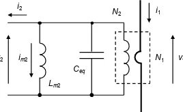
ZD1. Fig. 2 shows a CT equivalent circuit where Lm2 is the
secondary-side magnetizing inductance and Ceq is the
associated parasitic capacitance. v2 is the secondary terminal
voltage across N2. Fig. 3 shows the base driver circuit in [24]
driving a BJT in a buck converter. The drive signal is buffered by U1/2. The emitter-follower stage formed by TR3 and TR4 provides current pulses into and out of the base of TR1 at turn-on and turn-off respectively via the peaking circuit formed by Cp. R2 is included to provide damping [16], [25]. During TR1’s on-time, TR3/4 also provides a small base current into TR1 via R1 to accommodate any shortfall due to magnetizing current im2
[image:2.595.308.548.487.601.2]drawn by Lm2.
Fig. 1. Outline of base driver circuit with regenerative feedback using a current transformer from [24].
TR2 is a P-channel MOSFET. When TR1 is off TR2 is also held off. This prevents N2 from effectively forming a
short-circuit across -VDRI when the base of TR1 is low with respect to
0 V. When TR1 is on, TR2 is also on to allow a return path for the current supplied by CT1 into TR1’s base terminal.
Ideally the relationship between i2 and i1 is given by:
= (2)
and therefore:
t
actual i2with
component lost due to droop
Ton Toff Ton
i2
T=1/f
TR1 CT1
vBE
i2
Dr
iB
Driver circuit
ideal i2
i1= ic
N1 N2
VRESET
D1
= (3) but the presence of im2 affects this, and the equivalent circuit in
[image:3.595.305.547.297.543.2]Fig. 2 is applied here to cater for im2.
Fig. 2. CT equivalent circuit.
Importantly, the CT in Fig. 3 operates without a discrete voltage clamp for resetting its core flux during the BJT’s off-time. Instead, im2 is allowed to resonate in the LC circuit formed
by Lm2 and Ceq, and this is addressed in further detail in this
[image:3.595.51.289.351.543.2]section.
Fig. 3. Proposed driver circuit from [24].
Provided Dr can support the peak voltage v2(pk) reached, this
allows the reset voltage to be accumulated more rapidly than if a discrete clamping circuit were used. In [24] a maximum duty cycle δ exceeding 90% is readily attainable at a frequency of 50 kHz. Furthermore, only a modest voltage overshoot of approximately 1% was observed across the BJT at turn-off due to commutating the current in the CT’s leakage inductances in [24]. During the off-state D2 allows the driver stage to clamp TR1’s base to –VDRI and D4 allows Cp to discharge rapidly
through R2, thus allowing operation at a high δ.
The circuit in Fig. 3 can operate in three modes. These are the discontinuous magnetizing current mode (DMCM), the continuous magnetizing current mode (CMCM) and the discontinuous secondary current mode (DSCM). Fig. 4 shows a rectangular current waveform ip with a peak value Ip applied to
N1. ip’s period is T. The center waveforms show DMCM
operation. The bottom waveforms show CMCM operation. The ramp component in ip is neglected. Dr is rated to support v2(pk).
With respect to the DMCM mode in the center waveforms, im2
ramps up in Lm2 during Ton (Phase 1) and is lost from i2. At the
end of Ton, im2 has reached Im2(end), given by
( )= (4)
where Vf1 is the voltage across Lm2 during the current pulse. For
the circuit in Fig. 3, this is given by VBE(on) + Vf where Vf is the
forward voltage drop of Dr, and the voltage drops attributable to the on-state resistance of TR2 and N2’s resistance are
negligible. In the DMCM, im2 = 0 A at the beginning of the
current pulse. When Ip is removed there is a resonant exchange
of energy between Lm2 and Ceq during Phase 2. v2(pk) is given by:
Fig. 4. CT waveforms. Top: primary current (with ripple content neglected). Centre: waveforms with DMCM operation. Bottom: waveforms with CMCM operation.
( )=
−
(5) where fsw is TR1’s switching frequency. v2(pk) is fundamentally
independent of the magnitude of Ip as Vf1 does not vary
significantly with current. The frequency fres of the resonant
action is given by
= 1
2 (6)
and the resonant period Tres is the inverse of this. The damping
effect of core losses is neglected in (5) and (6). When the resonant half cycle has elapsed after a time Tres/2, Phase 3
commences. im2 then flows through Dr, D2 and the impedance
Ceq
N1
N2
v1
Lm2
i1
v2 im2
i2
TR1
ip
vBE
i2
DRIVE SIGNAL
v2
Dr CT1
D2 R1
D1
TR4 TR3
+VDRI
TR2
U1 U2
iLOAD
-VDRI
-VDRI
R2 Cp
D3 D4
VRAIL
vCE
t
v2 t im2 vf1
v2, im2 vf2
Im2(end)
Im2(0)
v2 t im2 v2, im2
Im2(end) ip
Ip
T (1-)T
tc
Phase 2
presented by the driver circuit which causes im2 to decay to zero
over a period tc. As TR2 is off during this phase, D3 provides a
return path for im2 to flow in N2. Whereas in the DMCM mode im2 decays to zero before the current pulse is re-applied, in the
CMCM mode im2 has not decayed to zero at this point. Although im2 passes through zero in the CMCM mode, the term
continuous is used here to refer to a state where im2 is only at
zero instantaneously.
In the DMCM mode, Im2(end) is given by (4). If Tres is taken as
much smaller than T, then in the CMCM mode, where Im2(0) is
the initial im2, Im2(end)can be found from
( )= ( )+ (7)
and
( )= − ( )+
(1 − )
. (8)
Combining (7) and (8) yields:
( )=2 (1 − ) + . (9)
Where δ tends to one then, provided the half-resonant period in Phase 2 is allowed to elapse fully,
( )=2 . (10)
Similarly, if Vf2 is close to Vf1 then when in the CMCM, Im2(end)
is also given by (10). The total (peak-to-peak) flux density swing ΔB in the CT’s core material for this scenario is given by
= (11)
where Ae is the CT core’s effective area. If Vf2 is much smaller
than Vf1 then
( )≅ 2 . (12)
The threshold duty cycle δTH at which the transition between the
DMCM and CMCM modes takes place is given by
= 1
1 + (13)
and if the ratio Vf1/Vf2 is expressed as k, then
= 1
1 + . (14)
In summary, with ideal resonant resetting and Vf2 ≤ Vf1, Im2(end) is always restricted to the value in (10), even for δ
approaching 100%. In the CMCM mode, the direction of im2
when Ip is applied is such that i2 exceeds the value given by (2).
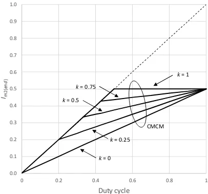
[image:4.595.49.287.224.338.2]That is, at the beginning of the current pulse, there is an initial oversupply of i2 as im2 has reversed. Fig. 5 shows Im2(end) against δ for different values of k for the idealized circuit operation in Fig. 4, where losses in the CT are neglected and T is taken as much greater than Tres/2. Quantities in Fig. 5 are normalized to
one, where Im2(end) in per-unit form Im2(end)(pu) is given by
( )( ) = . (15)
The curves for k = 1 and k = 0 in the CMCM mode represent the situations in (10) and (12) respectively. Curves for intermediate values of k of 0.25, 0.5 and 0.75 are also shown. If the series combination of Vf and VBE(on) is close to an ideal
voltage sink, then im2 is independent of i2. Minimizing Im2(end)
has the benefit that the current sourced through R1 to compensate for this loss in current from i2 can also be
minimized with a consequent reduction in losses.
B. CT Core Resetting with Discrete Clamp Circuitry and
Maximum Duty Cycle Considerations with Proposed Circuitry
1) Resetting with Discrete Clamp Circuitry
Power device duty cycles are typically limited to 50% in SMPS applications, but duty cycles close to 100% are normally essential in inverters. In Fig. 6 the effect of using a discrete circuit to apply a reset voltage vRESET is shown.
Fig. 5. Absolute droop in the form of Im2(end) normalized to one and plotted against δ for k between zero and one. In the DMCM mode Im2(end) is given by (4). In the CMCM mode Im2(end) is given by (9). δTH, where the transition between
the DMCM and CMCM modes occurs, is given by (13).
After an on-pulse ends, im2 has to be returned to 0 A or less
before Ip is re-applied otherwise CT core saturation will occur
over a few cycles. The decay in im2 to 0 A during Toff takes
longer (tc in Fig. 6) than that with resonant resetting. To avoid
CT core saturation, the maximum duty cycle δmax is limited to
= 1
1 +
. (16)
With resetting into a voltage VRESET, a lower-voltage rectifier
diode than that (Dr) in Fig. 3 can be used with the CT. However, a particular drawback in inverter applications is the lower δmax
attainable due to the longer minimum reset time tc needed. 0.0
0.1 0.2 0.3 0.4 0.5 0.6 0.7 0.8 0.9 1.0
0 0.2 0.4 0.6 0.8 1
Im2(
en
d
)
Duty cycle
k= 1
k= 0
k= 0.25
k= 0.75
k= 0.5
[image:4.595.327.530.330.519.2]Fig. 6. CT waveforms with discrete reset clamp circuitry.
2) Duty Cycle Considerations with Proposed Circuitry
With the circuit in Fig. 3, the behavior of the CT is only considered here for Toff ≥ Tres/2. That is, Ip is not reapplied until Tres/2 has elapsed and im2 has been able to reverse fully. Ipcan,
however, be reapplied between Tres/4 and Tres/2 (where a
quarter-cycle or a half-cycle respectively of the resonant action has elapsed) without core saturation occurring as im2 is returned
to 0 A or less. Waveforms for this scenario are shown in Fig. 7. However, a drawback is that, as Toff is reduced from Tres/2 to Tres/4, Im2(0) rises from the value in (8) to zero. Where im2(0) is
zero, it has not been reversed and the current Im2(end) lost into Lm2
at the end of Ton rises from the value given by (10) to that in (4).
Also, the peak voltage across Dr approximately doubles as v2(pk)
increases in magnitude. Furthermore, although there is little change in the total flux density swing, ΔB given by (11) in the CT’s core, the peak flux density reached with respect to zero increases from ΔB/2 to ΔB. For these reasons, δmax is taken as
(T- Tres/2)/T. If Toff is less than Tres/4, then CT core saturation
[image:5.595.307.545.369.574.2]results.
Fig. 7. Waveforms from circuit in Fig. 3 with Ip re-applied after im2 drops below 0 A, but before the half-resonant period Tres/2 elapses.
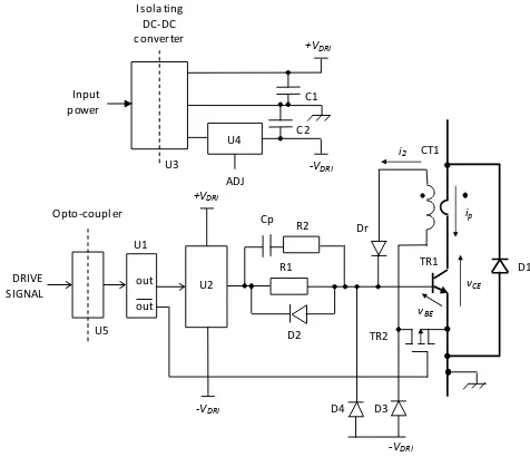
C. Circuitry Used for Experimentation
The experimental base driver circuit used in this paper is shown in Fig. 8. In [24] the circuit incorporated no galvanic isolation. However, in this paper, power is supplied to the circuit by means of a RECOM RB-0515D isolated-output DC-DC converter, U3, that has an isolation voltage rating of 1 kV and outputs voltages of +15 V and -15 V. The drive signal is transmitted by means of an HCPL3020 opto-coupler, U5, to provide isolation. U1 is an IX4426 driver IC with inverting and non-inverting outputs. The inverting output was used to drive
TR2 and the non-inverting output is fed to an IXDN614SI driver IC, U2, which was used to replace the emitter-follower stage in [24]. The signal for the base of TR2 was derived from a 4000-series inverter in [24], but this arrangement was replaced with U1 to give a higher voltage-handling capability. The positive voltage rail, +VDRI, is nominally 15 V and is
supplied directly by U3. However, the negative rail, nominally at -15 V from U3, is input to an LM337 linear voltage regulator, U4, to allow the base driver’s negative off-state voltage -VDRI to
be varied for experimentation.
Other data are: Cp = 22 nF, R2 = 2.2 Ω, R1 = 180 Ω, D2-4 = ES1A-13-F, Dr = IDD03SG60C, TR2 = FDT458P. C1 and C2 were 10-μF ceramic surface-mount types. The BJT does not have an intrinsic diode and the device used was not co-packaged with one, so a C4D15120D device was used in location D1 where a freewheeling function is needed. CT1 was constructed with a TN13/7.5/5 core in 3C90 material with a single primary turn and 43 secondary turns of 0.2-mm copper wire. The quoted inductance factor of the core is 1.17 μH/turn2 and this gives L
m2
= 2.16 mH. With Vf of Dr = 1 V and VBE(on) = 3 V, from (10)
this gives Im2(end) = 18.5 mA at fsw = 50 kHz and δ = 1, and if k
is taken as one. R1 was conservatively set to supply a compensating current of 67 mA.
Fig. 8. Outline of BJT base driver circuit with key components shown. A SiC Schottky diode is connected in parallel with the CT’s primary winding and the BJT when the BJT is used in a voltage source inverter.
III. EVALUATION OF THE OFF-STATE NEGATIVE BASE
-EMITTER VOLTAGE REQUIREMENT OF THE SICBJT
When rapid voltage changes are imposed across the power electrodes of a semiconductor device, unwanted turn-on may be induced due to current flowing into its control electrode through its Miller capacitance. Even where the controlling voltage at the device’s external terminals is held below the manufacturer’s quoted DC turn-on threshold voltage, turn-on can nonetheless still result. This is attributable to the internal impedance lying between the terminals and the active die area, and gate or base spreading resistances within the device.
t
vf1 v2
t im2 v2, im2
Im2(end) ip
Ip
T (1-)T
tc
vRESET
t
vf1 v2
t im2 v2, im2
Im2(end) ip
Ip
(1-)T T
Tres/2
TR1
ip
vBE
i2
DRIVE SIGNAL
Dr CT1
D2
R1 D1
U2
+VDRI
TR2
-VDRI
-VDRI
R2 Cp
D3 D4
vCE
U4
-VDRI
+VDRI
Opto-coupler Isolating
DC-DC converter
Input power
U3
U5
ADJ C1
C2
[image:5.595.72.271.464.601.2]As mentioned in Section I, experimental and theoretical studies have been carried out into the behavior of various power devices when subjected to dv/dt’s across their power electrodes, for example, the IGBT [26], and the SiC MOSFET [6], [7], [27]. However, less data is available for the SiC BJT and hence the study in this paper has been conducted.
Two GA06JT12-247 BJTs [28], TR1 and TR2, were configured in the test circuit in Fig. 9. The antiparallel diodes, D1 and D2, were C4D15120D types. TR2 was connected to the driver circuit in Fig. 8 and was driven on to apply a dv/dt across TR1, the device under test (DUT). TR1 was also driven with the circuit in Fig. 8 set in the OFF-state. This was to test the device with a typical driver circuit in place. vBE(1) was set at
different values by configuring U4 in TR1’s driver circuit as required. The CT in the driver circuit for TR1 was removed.
Double-pulse tests were then carried out and the displacement charge QD through TR1 was measured for various
conditions of temperature, rail voltage VRAIL and TR1’s
OFF-state vBE(1). An advantage of double pulse testing compared with
continuous operation is that the temperature of the heatsink on which the DUT is mounted can be readily set at different values with a resistive heater mounted onto the heatsink. The DUT’s die temperature will tend to follow that of the heatsink as the steady-state power dissipation is close to zero, and there is consequently little temperature gradient between the die and the temperature recorded on the heatsink’s surface. The dv/dt
applied to the DUT was not varied in these tests, but TR2 was driven to give a switching time of approximately 50 ns, corresponding to an average dv/dt≈ 20 V/ns when switching 600 V.
The current iU through TR1 was measured with a Rogowski
coil sensor to give QD. The current iC2 into TR2’s collector
terminal and the load current iLOAD were measured with DC
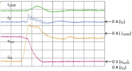
current probes. Exemplifying waveforms for vBE(1) = 4 V and
-14 V are shown in Figs. 10 and 11 respectively. In each case
VRAIL = 600 V and the heatsink temperature is 25°C. With vBE(1)
= -4V, it is seen that a transient current iU flows in TR1 during
the fall-time of vout. However this is significantly reduced with vBE(1) = -14V. As well as iU, it is noted that iC2 contains current
components due to charging and discharging the junction capacitances of D1 and D2 respectively, and a component due to charging stray capacitances associated with the load.
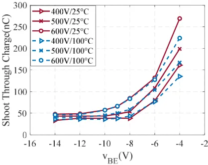
The measured QD is shown in Figs. 12 and 13. Fig. 12 shows QD plotted against vBE(1) at 400 V, 500V, and 600 V for
temperatures of 25°C, 50°C, 75°C and 100°C. Test results are given for -4 V to -14 V. In Fig. 13, the results at 25°C and 100°C have been superimposed. It is seen that there is little dependency on temperature, although at lower negative vBE(1)
values, a slight reduction in QD is observed at higher
temperatures. This is attributed to the fall in hFE with increased
[image:6.595.345.505.86.315.2]temperature. The maximum allowable negative base-emitter voltage of the device used is quoted at 30 V by the manufacturer [28] and applying a voltage of -14 V results in a safety margin of over 100%.
[image:6.595.311.539.359.476.2]Fig. 9. Circuit used for assessing behavior of the SiC BJT when subjected to a re-applied dv/dt.
Fig. 10. Exemplifying waveforms for vBE(1) = -4 V with VRAIL = 600 V and a
temperature of 25°C. Scales: iLOAD = 2 A/div., iU = iC2 = 5 A/div., vout =
200 V/div. Time scale: 50 ns/div.
Fig. 11. Exemplifying waveforms for vBE(1) = -14 V with VRAIL = 600 V and a
temperature of 25°C. Scales: iLOAD = iU = iC2 = 2 A/div., vout = 200 V/div. Time
scale: 50 ns/div.
TR2 CT1
vout
TR1 vBE(1)
Base driver circuit
VRAIL
D2
2.2Ω iLOAD
D1 1.4mH
25μF iU
[image:6.595.311.538.541.663.2](a) Displacement charge at 25°C.
(b) Displacement charge at 50°C.
(c) Displacement charge at 75°C.
(d) Displacement charge at 100°C.
Fig. 12. Displacement charge QD plotted against BJT base-emitter off-state
voltage for different conditions of rail voltage and temperature.
As expected, the curves of QD in Figs. 12 and 13 approach
plateaus as the reverse off-state base-emitter voltage of the DUT is increased. This is attributed to the charge drawn by the inter-terminal capacitances of TR1, and this component in QD
[image:7.595.76.259.89.719.2]cannot be eliminated by applying a negative off-state base-emitter voltage to the DUT.
Fig. 13. Superimposed test results at temperatures of 25°C and 100°C.
The power-dissipation Wst incurred in a phase-leg at turn-on
due to supplying a displacement charge into the complementary device in a VSC bridge leg is given by:
= . (17)
Taking the result at VRAIL = 600 V, vBE(1) = -4 V and a
temperature of 25°C, a displacement charge of 225 nC is measured, and this is reduced to 45 nC at vBE(1) = -12 V. At fsw
= 50 kHz this represents a loss reduction of 4.5 W, and a total of 13.5 W in a three-phase converter. In practice, however, Wst
is expected to be higher than the value predicted by (17) due to the modified switching trajectory introduced by the simultaneous conduction attributable to QD. This is seen in
Fig. 10 where QD is greater than that in Fig. 11, and the turn-on
trajectory of vout consequently differs.
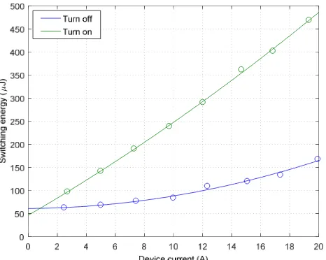
Before proceeding with inverter operation, the switching characteristics attainable with the proposed base driver were evaluated. The exemplifying waveforms in Fig. 14 show the BJT’s switching behavior at turn-on and turn-off. Fig. 15 shows switching energy for turn-on and turn-off plotted against the device current when operating at a supply voltage of 600 V [29]. Using the current transformer driver will reduce the turn-on loss due to the reductiturn-on of current overshoot but slightly increase the turn-off loss due to the voltage overshoot.
-16 -14 -12 -10 -8 -6 -4 -2
vBE(V)
0 50 100 150 200 250 300
400V 500V 600V
-16 -14 -12 -10 -8 -6 -4 -2
vBE(V)
0 50 100 150 200 250
Sh
oo
t T
hr
ou
gh
C
ha
rg
e(
nC
)/
75
°C 400V
500V 600V
-16 -14 -12 -10 -8 -6 -4 -2
vBE(V)
0 50 100 150 200 250
Sh
oo
t T
hr
ou
gh
C
ha
rg
e(
nC
)/
10
0°
C
[image:7.595.305.514.175.341.2]Fig. 14. Switching waveforms at turn-on (top) and turn-off (bottom). Vds1 and Id1 refer to vCE and ip respectively as shown in Fig. 8.
Fig. 15. Switching energy loss at turn-on and turn-off plotted against device current.
IV. APPLICATION OF THE SICBJT WITH PROPOSED BASE
DRIVER CIRCUIT IN AN INVERTER
[image:8.595.307.553.233.355.2]A three-phase two-level inverter using six of the switch modules in Fig. 8 was constructed, Fig. 16, where TR1 and D1 were GA06JT12-247 SiC BJTs and C4D15120D SiC Schottky diodes. A two-stage LC output filter was used and details are: L1 = L2 = L3 = 964.7 μH, C1 = C2 = C3 = 1.76 μF, L4 = L5 = L6 = 50 μH, C4 = C5 = C6 = 440 nF. The load was formed with three series LR circuits, Z1-Z3, connected in a star arrangement with L = 646 µH and R = 25 Ω. A photograph of the inverter is shown in Fig. 17.
Fig. 16. Experimental inverter.
VRAIL was 600 V and the nominal load of 4.1 kW was driven
with a modulation index M of 0.9. The control algorithm used dead-time compensation and third harmonic injection. The switching frequency was 50 kHz. Using the results in Section III, an off-state base-emitter voltage of -9 V was chosen for the BJT base drivers. This was selected to give an aggregate driver rail voltage of 24 V when added to the +VDRI of 15 V,
whilst eliminating most of the QD measured in the practical tests
in Section III. The resonant frequency fres of the CT was
observed at approximately 500 kHz during experimentation. This corresponds to a period Tres of 2 µs. In order to allow the
half-resonant period Tres/2 during Phase 2 in Fig. 4 to fully
elapse for the reasons given in Section II, a minimum off-time of 1 µs is therefore required. However, a safety margin was included and a minimum off-time of 2 µs was applied, hence giving a maximum δ, and therefore M, of 90% at 50 kHz.
Fig. 18 shows waveforms for a fundamental frequency of 400 Hz. iA, iB, iC are the three-phase output currents as denoted
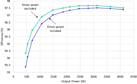
in Fig. 16. Fig. 19 shows graphs of the measured efficiency against load, with and without the power consumption of the base driver circuitry included. As the load-dependent component of the base current is supplied by the CT, the driver circuitry drew a power that was nearly constant over the load range and was measured at between 5.30 W and 5.37 W. The output phase current has an RMS value of 7.372 A, and therefore a peak value of 10.43 A. When developing the CT-based drive the BJTs’ hFE was taken as 43. An iB of 243 mA is
therefore required to cover the peak current. If this is set in the normal way, 243 mA is always being supplied into the base of one of the two devices in a phase-leg, apart from during dead-times. If this current is sourced from a 15-V supply, then each phase-leg needs to be supplied with 3.65 W, implying a total of
S1
S2 S3
S4 S5
S6 L1
L3 L2
L4
L6 L5
C1 C2
C3
VRAIL
C4 C5
C6 Z1
Z2
Z3
LOAD iA
iC
iB
[image:8.595.50.283.528.714.2]10.95 W solely to furnish the steady on-state iB currents. It is
noted that the total power drawn will exceed this due to the requirement to supply dynamic base-drive losses, and quiescent losses in the driver circuitry and DC-DC converter in Fig. 8.
With the CT-based drivers in place, a conservatively-set current of 67 mA is being supplied through R1 in Fig. 8 to the base of one of the BJTs in each phase-leg at any given time. This equates to 1.005 W per phase when supplied from 15 V, and 3.02 W for all three phase-legs. The external power supply therefore only has to supply 28% of the original power of 10.95 W required for driving the steady-state base currents.
Efficiency was measured with two Norma 4000 units. One was used to measure the 3-phase output power. The other was used to measure the power from the DC link power supply and the power drawn by the driver circuits. The measured full-load quantities were as follows, where the efficiency figure quoted takes into account the power consumption of the base driver circuitry:
DC link voltage VRAIL: 599.8 V
DC input current: 7.044 A Input power: 4.221 kW Output phase voltage: 188.1 V Output phase current: 7.372 A Output apparent power: 4.160 kVA Output active power: 4.117 kW Efficiency: 97.4%
[image:9.595.311.546.90.213.2]As seen, the three-phase SiC inverter can operate successfully with the presented base driver and negative OFF-state voltage, and an overall full-load efficiency of 97.4% has been obtained at a 50-kHz switching frequency, with the base driver power consumption accounted for. A fan was used to provide forced cooling of the heatsink in Fig. 17. The power consumption of the fan was measured at 1.05 W and this was included in the efficiency calculation.
[image:9.595.311.545.253.398.2]Fig. 17. Experimental inverter showing power devices mounted onto heatsink and base driver circuits.
Fig. 18. Output current waveforms from circuit in Figs. 16 and 17. Scales: iA = iB = iC = 5 A/div. Time scale: 500 μs/div.
Fig. 19. Efficiency against output power.
V. DISCUSSION
Whilst the high duty cycle operation needed for an inverter application is possible, the duty cycle is nonetheless limited to less than 100% due to the need for CT reset. As well as increasing the headroom voltage required by the converter, this precludes the use of dead-banding techniques such as [30]. Complementary drive signals were applied to both devices in each phase-leg throughout the entire 360° base frequency cycle. As the SiC BJT cannot effectively conduct in reverse, the power dissipation in the device and its base driver circuitry can be reduced by applying one-step commutation [31]. With this technique, BJTs in locations where the associated anti-parallel diode is conducting are not driven on. However, knowledge of the load current direction is required. A feature of the proposed circuitry is that the CT is located directly in series with the BJT and automatically regulates the bulk of the base current in response to the collector current. Advantageously, this means that when the BJT is freewheeling, the load current flows in reverse through the anti-parallel diode. Even without one-step commutation being implemented, a power saving is attained as the only losses are those associated with driving transient currents into the base, and the small component sourced via R1. The power consumption of base driver circuits with and without a CT have been compared when driving the inverter at its rated load, and when sourcing a phase current of 7.372 A. However, this does not take into account the possibility of short-term transient operation with a higher phase current. In this case, the driver circuitry without the CT would have to be
0 A
iA iB iC
93 93.5 94 94.5 95 95.5 96 96.5 97 97.5 98
0 500 1000 1500 2000 2500 3000 3500 4000 4500
Ef
fic
ie
nc
y
(%
)
Output Power (W) Driver power
included Driver power
[image:9.595.82.254.519.658.2]configured to source a base current higher than 243 mA. Consequently, the power consumption would be higher than the 10.95 W calculated. Conversely, the CT-based circuit automatically supplies higher base currents under such conditions without the penalty of higher power consumption being incurred during normal operation.
A minimum switch off-time of 2 µs was imposed to accommodate CT reset, and increased harmonic content is expected in the AC current waveform as the minimum off-time increases. However, as mentioned in Section IV, a minimum off-time of only 1 µs was observed to be necessary, and the safety margin of 100% that was applied here is conservative. Also, simple PWM was used without incorporating any of the available compensation schemes for reducing harmonic content. Using deadtime compensation schemes will be future work to compensate the harmonic content and output voltage reduction. A further issue with applying minimum off-times is that a higher DC bus voltage is required for a given output AC voltage, with the corollary of higher switching losses in the BJTs. As such, there is a trade-off between the driver stage losses and switching losses with the proposed circuitry. However, in some applications the existing bus voltage will be at a level higher than that needed to provide the maximum AC voltage required. Also, by reducing the gate driver losses and power requirement using the proposed circuit in this paper, a standard gate driver power supply can be used, rather than using a special high power supply. It is noted that the CT’s design has not been optimized to maximize its resonant frequency fres for a
given droop, and increasing fres reduces the reset time, and
therefore the minimum off-time required.
A like-for-like comparison between a 4-kW 3-phase SiC MOSFET based converter and a 3-phase SiC BJT based converter is given in [29]. As shown in [29], the SiC BJT and SiC MOSFET converter have very similar efficiencies, i.e. 97.3% for the BJT converter and 97.65% for the MOSFET converter at 50-kHz switching frequency. Normally, an efficiency above 97% is required for the power stage to meet the power loss and cooling requirement. Therefore, the maximum switching frequency of SiC MOSFET and BJT converters should be around 60 kHz~70 kHz to meet the efficiency requirement, also noting that adjusting the gate driver/resistance, or using soft-switching may push these switching frequencies even higher.
VI. CONCLUSION
Displacement currents in the SiC BJT due to dv/dt-induced conduction may be readily eliminated by applying a negative off-state base-emitter voltage. For the device investigated here, this voltage has been experimentally assessed for switched voltages of 400 V, 500 V, and 600 V, and at device temperatures of 25°C, 50°C, 75°C, and 100°C. A base-emitter voltage of -1µV or lower was found to be sufficient to suppress dv/dt-induced conduction for dv/dt’s up to approximately 20 V/ns when driven from a 600-V rail. The SiC BJT used has a maximum quoted negative base-emitter voltage of 30 V. Unlike the SiC MOSFET, there is therefore little compromise required between avoiding exceeding the rated negative control
electrode voltage and applying sufficient voltage to hold the device off. The efficacy of using a regenerative proportional base driver circuit with a CT in an inverter application has been demonstrated. The difficulty encountered in attaining high duty cycles is addressed by configuring the CT in a driver circuit allowing resonant resetting.
REFERENCES
[1] C. DiMarino, R. Burgos, and D. Boroyevich, “High-temperature silicon carbide: characterization of state-of-the-art silicon carbide power transistors,” IEEE Ind. Electron. Mag., no. 3, pp. 19-30, Sep. 2015. [2] J. Rabkowski, D. Peftitsis, and H.-P. Nee, “Silicon carbide power
transistors: a new era in power electronics is initiated,” IEEE Ind. Electron. Mag., vol. 6, no. 2, pp. 17-26, Jun. 2012.
[3] S. Hazra, S. Madhusoodhanan, G. Karimi Moghaddam, K. Hatua, and S. Bhattacharya, “Design considerations and performance evaluation of 1200-V 100-A SiC MOSFET-based two-level voltage source converter,” IEEE Trans. Ind. Appl., vol. 52, no. 5, pp. 4257-4268, Sep./Oct. 2016. [4] G. Calderon-Lopez and A. J. Forsyth, “High power density DC-DC
converter with SiC MOSFETs for electric vehicles,” in Proc. IET 7th Power Electron., Machines and Drives Conf., Manchester, UK, April 2014.
[5] R. Ouaida et al., “Gate oxide degradation of SiC MOSFET in switching conditions,” IEEE Electron. Device Lett., vol. 35, no. 12, pp. 1284-1286, Dec. 2014.
[6] S. Jahdi et al., “Temperature and switching rate dependence of crosstalk in Si-IGBT and SiC power modules,” IEEE Trans. Ind. Electron., vol. 63, no. 2, pp. 849-863, Feb. 2016.
[7] R. Khanna, A. Amrhein, W. Stanchina, G. Reed, and Z.-H. Mao, “An analytical model for evaluating the influence of device parasitics on Cdv/dt induced false turn-on in SiC MOSFETs,” in Proc. IEEE 28th Annu. Appl. Power Electron. Conf. and Expo., Long Beach, CA, USA, pp. 518-525, Mar. 2013.
[8] P. Anthony, N. McNeill, and D. Holliday, “High-speed resonant gate driver with controlled peak gate voltage for silicon carbide MOSFETs,” IEEE Trans. Ind. Appl., vol. 50, no. 1, pp. 573-583, Jan./Feb. 2014. [9] Y. Gao, A. Q. Huang, A. K. Agarwal, and Q. Zhang, “Theoretical and
experimental analyses of safe operating area (SOA) of 1200-V 4H-SiC BJT,” IEEE Trans. Electron Devices, vol. 55, no. 8, pp. 1887-1893, Aug. 2008.
[10] G. Calderon-Lopez, A. J. Forsyth, D. L. Gordon, and J. R. McIntosh, “Evaluation of SiC BJTs for high-power DC-DC converters,” IEEE Trans. Power Electron., vol. 29, no. 5, pp. 2474-2481, May 2014. [11] D. Peftitsis, J. Rabkowski, G. Tolstoy, and H.-P. Nee, “Experimental
comparison of Dc-Dc boost converters with SiC JFETs and SiC bipolar transistors,” in Proc. 14th European Conf. on Power Electron. and Appl., Birmingham, UK, Aug./Sep. 2011.
[12] S. Safari, A. Castellazzi, and P. Wheeler, “Experimental and analytical performance evaluation of SiC power devices in the matrix converter,” IEEE Trans. Power Electron., vol. 29, no. 5, pp. 2584-2596, May 2014. [13] A. Hensel, C. Wilhelm, and D. Kranzer, “Development of a boost
converter for PV systems based on SiC BJTs,” in Proc. 14th European Conf. on Power Electron. and Appl. Birmingham, UK, Aug./Sep. 2011. [14] M. M. R. Ahmed, N.-A. Parker-Allotey, P. A. Mawby, M. Nawaz, and C.
Zaring, “Characterization of the static and dynamic behavior of a SiC BJT,” in Proc. 13th Int. Power Electron. and Motion Control Conf., Poznań, Poland, pp. 2472-2477, Sep. 2008.
[15] R. Singh, S. Sundaresan, E. Lieser, and M. Digangi, “1200 V SiC “super” junction transistors operating at 250 °C with extremely low energy losses for power conversion applications,” in Proc. IEEE 27th Ann. Appl. Power Electron. Conf. and Expo, Orlando, FL, USA, pp. 2516-2520, Feb. 2012. [16] J. Rabkowski, G. Tolstoy, D. Peftitsis, and H.-P. Nee, “Low-loss
high-performance base-drive unit for SiC BJTs,” IEEE Trans. Power Electron., vol. 27, no. 5, pp. 2633-2643, May 2012.
[17] H. Choi, “Overview of silicon carbide power devices,” www.fairchild.com, accessed Jun. 2017.
[19] L. Liao et al., “A new proportional base drive technique for SiC bipolar junction transistor,” IEEE Trans. Power Electron., vol. 32, no. 6, pp. 4600-4606, Jun. 2017.
[20] R. A. Dunipace, “SiC proportional bias switch driver circuit with current transformer”, US Patent Application No. US 2014/0035627, 6 Feb. 2014. [21] A. Akademir, “Enhanced regenerative switching circuit for power transistors,” IEE Electron. Lett., vol. 19, no. 16, pp. 631-632, 4 Aug. 1983.
[22] I. Takahashi, J. Itoh, and G. J. Su, “Toward 99% efficiency for transistor inverters,” IEEE Ind. Appl. Mag., vol. 2, no. 6, pp. 39-46, Nov./Dec. 1996.
[23] Z. Zhang, F. Wang, L. M. Tolbert, and B. J. Blalock, “Active gate driver for crosstalk suppression of SiC devices in a phase-leg configuration,” IEEE Trans. Power Electron., vol. 29, no. 4, pp. 1986-1997, Apr. 2014. [24] N. McNeill, B. Jin, and X. Yuan, “Proportional regenerative base driver
circuit with negative off-state voltage for SiC bipolar junction transistors,” in Proc. IET 8th Power Electron., Machines and Drives Conf., Glasgow, Scotland, Apr. 2016.
[25] D. Peftitsis and J. Rabkowski, “Gate and base drivers for silicon carbide power transistors: An overview,” IEEE Trans. Power Electron., vol. 31, no. 10, pp. 7194-7213, Oct. 2016.
[26] N. McNeill, K. Sheng, B. W. Williams, and S. J. Finney, “Assessment of off-state negative gate voltage requirements for IGBTs,” IEEE Trans. Power Electron., vol. 13, no. 3, pp. 436-440, May 1998.
[27] Q. Yan, X. Yuan, Y. Geng, A. Charalambous, and X. Wu, “Performance evaluation of split output converters with SiC MOSFETs and SiC schottky diodes,” IEEE Trans. Power Electron., vol. 32, no. 1, pp. 406-422, Jan. 2017.
[28] GA06JT12-247 datasheet, www.genesicsemi.com, accessed Jul. 2017. [29] I. Laird, B. Jin, N. McNeill, and X. Yuan, “Performance comparison of
3-phase DC/AC converters using SiC MOSFETs or SiC BJTs,” in Proc., IEEE 43rd Ann. Conf. IEEE Ind. Electron. Soc., Beijing, China, Oct./Nov. 2017.
[30] V. G. Agelidis, P. D. Ziogas, and Geza Joos, ““Dead-band” PWM switching patterns,” IEEE Trans. Power Electron., vol. 11, no. 4, pp. 522-531, Jul. 1996.
[31] H. Barth and W. Hofmann, “Decrease of SiC-BIT driver losses by one-step commutation,” in Proc. 2014 Int. Power Electron. Conf., Hiroshima, Japan, pp. 2881-2886, May 2014.
Neville McNeill received the Ph.D. degree in
power electronics from Napier University, Edinburgh, U.K., in 2008.
He has worked for electric vehicle and renewable energy companies, and from 2004 to 2016 he was at the University of Bristol, Bristol, U.K., where he was latterly Senior Lecturer in Power Electronics. Since 2016 he has been Senior Research Fellow in Power Electronics with the Power Electronics, Drives and Energy Conversion (PEDEC) group in the Department of Electronic and Electrical Engineering at the University of Strathclyde, Glasgow, U.K. His main research interest is in the application of wide-bandgap and silicon devices to realize high-efficiency multi-kilowatt power electronic conversion for aerospace, renewable energy, and electric vehicle applications.
Dr. McNeill is a Member of the Institution of Engineering and Technology, a Chartered Engineer with the Engineering Council of the U.K., and a Fellow of the Higher Education Academy.
Bosen Jin received the B.S. degree from
Northumbria University, Newcastle, U.K. and the M.Sc. degree from University College London, London, U.K., in 2012 and 2013, respectively, both in electrical engineering.
He is currently pursuing the Ph.D. degree at the Electrical Energy Management Group, University of Bristol, Bristol, U.K. His research interests include multilevel converter topologies and controls, power loss modelling and analysis.
Xibo Yuan (S'09-M'11-SM'15) received the B.S.
degree from China University of Mining and Technology, Xuzhou, China, and the Ph.D. degree from Tsinghua University, Beijing, China, in 2005 and 2010, respectively, both in electrical engineering.
He has been a Professor since 2017 in the Electrical Energy Management Group, Department of Electrical and Electronic Engineering, University of Bristol, Bristol, U.K., where he became Lecturer, Senior Lecturer and Reader in 2011, 2015 and 2016, respectively. He also holds the Royal Academy of Engineering/Safran Chair in Advanced Aircraft Power Generation Systems. He is an executive committee member of the UK National Centre for Power Electronics and the IET Power Electronics, Machines and Drives (PEMD) network.
His research interests include power electronics and motor drives, wind power generation, multilevel converters, application of wide-bandgap devices, electric vehicles and more electric aircraft technologies. Professor Yuan is an Associate Editor of IEEE Transactions on Industry Applications and IEEE Journal of Emerging and Selected Topics in Power Electronics. He is a Fellow of the IET and received The Isao Takahashi Power Electronics Award in 2018.
Ian Laird (S'09-M'11) received both the B.Eng.
degree (Hons. I) in mechatronic engineering in 2008 and the Ph.D. degree in electrical engineering (power electronics) in 2013 from the University of Sydney, NSW, Australia.
![Fig. 1. Outline of base driver circuit with regenerative feedback using a current transformer from [24]](https://thumb-us.123doks.com/thumbv2/123dok_us/1346313.88311/2.595.308.548.487.601/outline-driver-circuit-regenerative-feedback-using-current-transformer.webp)