International Journal of Innovative Technology and Exploring Engineering (IJITEE) ISSN: 2278-3075, Volume-8 Issue-7, May, 2019
Abstract:Hybrid Electric vehicles are the key sector in vehicle industries owing to zero emission, and fuel optimization. Power electronic converters plays essential role in electric vehicles to improve efficiency and meet the desired performance characteristics. Boost inverters may be utilized as power electronics converters in electric vehicles. This inverter is a single stage DC –AC converter with voltage boosting ability also.It has major merits of compact size, less weight, less volume, high efficiency, etc. as compared with the double stage conventional converter. This paper presents the experimental as well as simulation analysis of single phase single stage boost inverter with resistive load .It is proved that desired voltage, current waveforms with suitable values has been achieved, also various performance parameters has been evaluated and good results are achieved.
Index Terms: Boost Converter,Boost Inverter,Hybrid Electric Vehicles,THD.
.
I. INTRODUCTION
Electric vehicles are the one of the most emerging technology of transportation sector. Power electronics converters are major part of electric vehicle .boost inverter may provide important benefits such as single stage conversion, low cost, compact size, and high efficiency as a power electronic converter systems.
A. Motivation-
The most challenging problem in the world is vehicle pollution. As population is increasing vehicle is increasing in the road by leaps and bond.In order to arrest this problem electric vehicle is one of the feasible solution.
Power electronic which consist of high powers switches and power converters plays vital role in design of electric vehicles.In this work a power electronic converter known as boost inverter has been designed and experimented in the power electronic lab. This converter is different from basic inverter because conventional inverters are buck inverters whereas this is a boost inverter and second thing, it is single stage, so there is double advantage of this inverter.
Revised Manuscript Received on May 10, 2019
Piyush Kumar Ojha Mr. Piyush Kumar Ojha has completed B.Tech degree from United college of Engineering and Research, Allahabad.
Dr. Parashuram Thakura B.Sc Engg (Electrical) from National Institute of Technology Jamshedpur in 1986 and ME in Electronics and Control from Birla Institute of Technology Pilani Rajasthan
B. Literature survey-
A new configuration of DC to AC converter is proposed in paper which produces AC voltage at the output terminal with buck boost property depending upon the duty ratio. Suitable controller design is also needed [1] Sliding mode controller approach is utilized to control the plant parameter, whereas this process of control lack to control inductor current directly. [2] A new double loop control scheme is presented which consists of the inner control loop of inductor current and outer control loop of output voltage [4]. Three phase boost inverter supplied to the fuel cell used as stand-alone power source. Boosting and DC to AC conversion occurs in single stage having benefits of low cost, compact [7] Dynamics linearizing modulator based control strategy is applied to condition dual boost inverter for dynamic voltage and current load [6].
The closed loop waveform control of boost inverter is approached to reduce or eliminate the AC ripple component of the input current of single phase boost inverter [11] Half cycle modulation concept is applied to boost inverter to reduce the conduction and switching losses of systems [10]. A high gain single stage boost inverter with lower component count is being discussed to generate AC voltage. Single phase boost inverter along with coupled inductor with high boost gain and improved stability of output voltage achieved is proposed [5]. Design and development of adaptive control technique and fuzzy neural network control process for a single stage boost inverter is considered and compared. [8]
The single stage boost inverter with coupled inductor has been presented in paper. This paper described the modeling of coupled inductor single stage boost inverter and power loss analysis.[15].
A new single phase switched boost inverter with four switches is introduced in paper.it has main attributes of continuous input current ,boost voltage capability with one stage conversion, and shoot through immunity[16].
A new proportional resonant controller is proposed to reduce the dc offset and clipping effect arises due to dead time phenomenon and to achieve zero steady state error [17].
One cycle control approach, a nonlinear control technique used to track a dc biased sinusoidal voltage as a control reference. The benefit of the approach is easy implementation with a
simple circuit [18].
Single Phase Single Stage Boost Inverter for
Hybrid Electric Vehicles
C. Major contribution-
Major contribution of the work presented in this paper are as follows-
• Application of simulation platform on single phase boost inverter to obtain various waveform of desired nature.
• Design of single phase single stage boost inverter circuit arrangement, experimentation and testing to verify simulation process.
Analysis of various output waveforms obtained from single phase boost inverter, evaluation of THD for desired results.
D. Organization-
Section II describes the idea about the configuration of boost inverter and its operating principle. Section III gives the idea about the boost inverter electrical network. Section IV illustrates the simulation circuit at switching frequency of 50 Hz with DC input supply voltage of 12 Volt. Section V presents the analysis of boost inverter simulation with DC input supply voltage of 24 Volts. Section VI provides hardware details and experimentation process details. Section VII gives the results data discussion about various output nature. Section VIII concludes the analysis of a boost inverter with usage.
II. CONFIGURATIONOFBOOSTINVERTER
The DC-DC boost inverter basically consists of two boost converters connected in a differential manner across the load terminal. This configuration may be presented as below-
Fig.1. Block Diagram presentation of boost inverter
Expression for Instantaneous Output voltage
Vx -Voltage produced from converter X
Vy –Voltage generated from converter Y
Vk - The value of DC bias voltage
Xm -Peak value of sine wave
Expression for Average Output voltage-
Where
-Input DC voltage,
-Duty ratio
The converter X will produce DC biased sine wave signal and converter Y will also generate DC biased sine wave data while the output of converter X and converter are 180 degrees out of phase with respect to each other.
III. BOOSTINVERTERELECTRICALNETWORK
The Boost Inverter Electrical network is shown in figure2. It consists of two inductors connected at supply terminal as energy boosting elements.
Fig.2. Boost inverter Electrical Circuit
A. Operation Principle of boost inverter-
Every boost inverter circuit basically composed of two boost converter. The circuit operation may be easily understood by taking converter X as given in fig.3.
International Journal of Innovative Technology and Exploring Engineering (IJITEE) ISSN: 2278-3075, Volume-8 Issue-7, May, 2019
It has two parts of operations-
Part 1-
Switch SW1 is closed and SW2 is in an open condition. The current through inductor L1, iL1 increases with linear nature,
D2 the diode will be turned off due to reverse biased
condition. Capacitor C1 gives its stored energy to the load
terminal, thereby voltage V1 decreases.
Part2-
Switch SW2 is turned on and switch SW1 turned off. The current through inductor iL1 flowing through C1 and the load
terminal, in this way the capacitor C1 is recharged and current
iL1 starts decreasing.
IV. SIMULATION ANALYSIS
Figure 4 shows the diagram of Simulink model of a single phase boost inverter with an input supply terminal voltage of Vs =12V.
[image:3.595.307.538.49.156.2]Fig.4. Simulation of Circuit Diagram of Single Phase Boost Inverter
Figure 5 depicts the waveform of supply voltage, it is a DC waveform having the magnitude of 12 V, and fig 6 is the nature of supply current waveform.
Fig.5.Supply voltage of boost inverter
[image:3.595.49.288.310.491.2]Fig.6. Input supply current of boost inverter
Fig.7.Voltage across Load terminal
Fig.8. Current through load resistance
Fig.9.Voltage across capacitor1 (Vc1)
[image:3.595.47.291.589.726.2]Fig.11.Inductor current (IL1)
[image:4.595.279.542.314.729.2]Fig.12.Inductor current ( IL2)
Fig.13.FFT analysis of output voltage
Fig.14.FFT analysis of output current
Figure 7 presents the waveform of output voltage with respect to time and Figure 8 shows the wave shape of output current through load resistance with respect to time. Waveform of output voltage shows that the peak value of output waveform is 40volt and peak value of output current is 0.1 ampere. The nature of wave shape is sinusoidal nature. Capacitor voltage Vc1 and Vc2 are phase shifted with each other.Vc1 and Vc2 having unidirectional and positive values.
shown in figure 11 and figure 12 respectively. The inductor currents are increasing and decreasing in linear manner.
FFT analysis of output voltage obtained from MATLAB is shown in figure13.The THD of output voltage is 4.21% which can be acceptable. THD analysis of output current is given in figure 14 .THD of output current is 4.21% and is also good factor.
V. SIMULATION ANALYSIS WITH24VDCSUPPLY
Figure 15 shows the waveform of supply voltage, the value of supply voltage is 24V DC. Output voltage across load terminal is shown in figure 17.The peak voltage level of output voltage is 80 volt. The output current trough load resistance is shown in figure 18.The peak value of output current is 0.2 ampere. Figure 19 and figure 20 depicts the wave shape of capacitor voltage VC1 across capacitor C1 and
capacitor voltage VC2 across capacitor C2.Inductor current
IL1 and IL2 is shown in figure21 and figure 22 respectively.
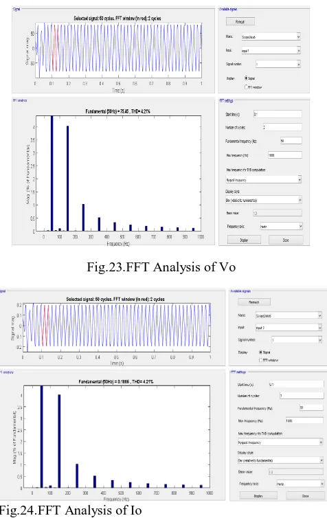
THD of output voltage and also output current is 4.21% as given by figure23and figure 24 respectively.
Fig.15 supply DC voltage
Fig.16 supply input current
[image:4.595.48.294.469.611.2]International Journal of Innovative Technology and Exploring Engineering (IJITEE) ISSN: 2278-3075, Volume-8 Issue-7, May, 2019
Fig.18. output current
Fig .19.Capacitor voltage Vc1
Fig .20.Capacitor voltage Vc2
Fig.21.Inductor current IL1
[image:5.595.309.547.47.424.2]Fig.22.Inductor current IL2
Fig.23.FFT Analysis of Vo
Fig.24.FFT Analysis of Io
VI. EXPERIMENTAL SETUP
The hardware set up of single phase boost inverter has been prepared according with selected parameters of inverter .hardware circuit of boost inverter possesses two important portion and these two part of the circuit are called as power unit and control or firing unit.
Firing Unit-
The firing or triggering pulses which will turn on and turn off the power switching devices are being generated by arduino microcontroller through appropriate programming. The four firing pulses g1, g2,g3 and g4 are produced from
[image:5.595.49.288.57.346.2]Fig. 25 TLP-250 Pin Diagram Power unit-
[image:6.595.56.284.255.391.2]Power unit consist of four power semiconductor devices as switches, two inductors, two capacitors and resistance as load.
Fig.26 Output voltage across load resistance measured from power analyzer
[image:6.595.54.284.438.583.2]Fig.27 output voltage and output current waveform taken from power analyzer
Fig.29 inductor current waveform
Fig.30 THD analysis observed from Power analyzer
Fig.31 Experimental arrangement of Single phase boost inverter
T
Single phase boost inverter circuit has been built and then experimentation has been conducted. Figure 31 shows the picture of experimental set up of single phase boost inverter. The experimental stage of single phase boost inverter consists of following steps-1. The DC input supply is given to the input terminal of the inverter and the firing pulses are also fed to the gate terminals of the power switches simultaneously.
2. The output voltage at the load terminal, output current through load resistance has been measured from power analyzer.
3. The capacitor voltages across capacitors C1 and C2 and
inductor currents through inductors L1 and L2 has been
measured from power analyzer.
[image:6.595.56.282.623.765.2]International Journal of Innovative Technology and Exploring Engineering (IJITEE) ISSN: 2278-3075, Volume-8 Issue-7, May, 2019
The output current is shown in fig.27.It is in the same phase with output voltage due to resistive load .the power factor is unity. The RMS value of output current is 0.4 ampere at 49.68Hz.The capacitor voltage Vc is drawn in fig28.it is unidirectional with DC bias. The inductor current is shown in fig29.it has the rms value of 6 ampere at 49.91Hz.
The harmonic analysis of output voltage obtained with power analyzer is shown in fig30. The total harmonic distortion is only2.91%., which is very acceptable and desired value.
VII. RESULT
Table1-parameter values of boost inverter
S.N
o.
Parame
ter
Simulati
on
Value at
12 V
Simulati
on
Value at
24 V
Experime
ntal Result
at 50V
1
Vs
12 V
24 V
50 V
2
Vo
28.28V
56 V
73.1 V
3
fs
50 Hz
50 Hz
50 Hz
4
fo
50 Hz
50 Hz
50 Hz
5
R
400
Ω
400
Ω
500
Ω
6
L1,L2
10 mH
10 mH
21 mH
7
C1,C2
600 µF
600 µF
300 µF
8
Io
0.07A
0.14 A
0.4 A
Table 1 depicts the various case study results at different supply voltages. Column 1 and column 2 of table 1 shows the result obtained from simulation process whereas column 3 gives the output data with experimental means. We may conclude that the rms value of output AC voltage at output terminal is greater than the input DC voltage applied at input terminal
.
VIII. CONCLUSION
The boost inverter perform the DC to AC conversion and voltage boosting phenomenon simultaneously and with one stage process. The same action has been verified with simulative analysis given in this paper for DC supply voltage of Vs=12Volt, Vs=24Volt and experimental result with applied input DC voltage of Vs=50Volt.The boost inverter circuit application includes the power conversion unit in hybrid electric vehicles, AC motor drives ,uninterrupted power supplies etc. The merit of single phase inverter having boosting ability in one stage are low cost, compact system configuration, high efficiency etc.
The experimental set up of single phase boost inverter has been prepared and tested in power electronic laboratory.
After DC input supply is given to input terminal, output has been tested/measured at output terminal and output current ,output voltage wave shape has been derived from power analyzer and shown in fig27.This result verifies that the output voltage and output current are desired one. It means output voltage and current waveform is sinusoidal in nature. Thus input DC voltage is converted to output sine voltage and
also the RMS value of output voltage is 73 Volt from input voltage of 50 Volt. Thus one important aspect of this experiment is that the output voltage is boosted from 50 V to 73 V.
Therefore this inverter convert DC voltage to AC voltage and also boost up of voltage has been done in one stage only. Thus the earlier mentioned process is verified through experimental means(data).Simulation process of boost inverter also provides the data which shows the output voltage is sine wave shape with higher value from DC input value.
Various waveforms such as capacitor voltage, inductor current, input current has been obtained through simulation and experimental process and their waveform nature and values are desired one. Total harmonic distortion THD of output voltage is also low value which is required one.
REFERENCES
1. R. O. Caceres and I. Barbi, “A Boost DC - AC Converter: Operation, Analysis, Control and Experimentation.,” Proc. IEEE IECON’95 Conf., Orlando, FL, Nov. 5–11, pp. 546–551, 1995.
2. R. O.Caceres and I. Barbi, “A Boost DC – AC Converter : Analysis , Design , and Experimentation,”in IEEE Trans. Power Electron., vol. 14, no. 1, pp. 134–141, 1999.
3. C. Cecati, S. Member, A. D. Aquila, and M. Liserre, “A Novel Three-Phase Single-Stage Distributed Power Inverter,” in IEEE Trans. Power Electron., vol. 19, no. 5, pp. 1226–1233, 2004.
4. P. Sanchis, A. Ursæa, E. Gubía, and L. Marroyo, “Boost DC – AC Inverter : A New Control Strategy,”in IEEE Trans. Power Electron., vol. 20, no. 2, pp. 343–353, 2005.
5. Y. Zhou, S. Member, and W. Huang, “Single-Stage Boost Inverter With Coupled Inductor,”in IEEE Trans. Power Electron., vol. 27, no. 4, pp. 1885–1893, 2012.
6. K. Jha and S. Mishra, “A Dynamic Linearizing Modulator based Boost Inverter,”in IEEE Applied Power Electronics Conference and Exposition(APEC), no. i, pp. 2369–2373, 2013.
7. M.Jang and V.G.Agelidis, "A Boost-Inverter-Based, Battery-Supported,Fuel-Cell Sourced Three-Phase Stand-Alone Power Supply," in IEEE Trans. Power Electron. ,vol.29,no.12,pp.6472-6480,2014.
8. R. Wai, S. Member, Y. Lin, and Y. Liu, “Design of Adaptive Fuzzy-Neural-Network Control for a Single-Stage Boost Inverter,” in IEEE Trans. Ind. Electron. vol. 30, no. 12, pp. 7282–7298, 2015. 9. Y. Tang, X. Dong, and Y. He, “Active Buck – Boost Inverter,” in IEEE
Trans. Ind.Electron. vol. 61, no. 9, pp. 4691–4697, 2014.
10. Y. Tang, Y. Bai, J. Kan, and F. Xu, “Improved Dual Boost Inverter With Half Cycle Modulation,” in IEEE Trans. Power Electron., vol. 32, no. 10, pp. 7543–7552, 2017.
11. G. Zhu, C. Xiao, H. Wang, and S. Tan, “Closed-loop waveform control of boost inverter,” in IET Power Electron.,vol. 9, pp. 1808–1818, 2016. 12. M.Kumari,P. R. Thakura,and D N Badodkar "Transient Analysis of Three-Phase High-Power Voltage Source Inverter with Nonlinearities in Hybrid Electric Vehicle," in IEEETrans.Power Electron.,vol.33,no.4,pp.3672-3680,2018.
13. A.Alam,M. K. Mukul,and P. R. Thakura,"Wavelet Transform-Based EMI Noise Mitigationin Power Converter Topologies"in IEEE Trans. Electromagnetic Compatibility,vol.58,no.5,pp.1662-1673,2016. 14. M.H. Rashid, "Power Electronics : Circuits Devices and Applications",
3rd ed.,Pearson,2009.
15. Y.Zhou,W.Huang,F.Hong,andC.Wang, "Modelling analysis and power loss of coupled -inductor single -stage boost inverter based grid-connected photovoltaic power system" in IET Power Electron.,vol.9,no.8,pp.1664-1674,2016.
16. M.K.Nguyen,andT.T.Tran "A Single -Phase Single- Stage Switched- Boost Inverter with Four Switches" in IEEE Trans. Power Electron.,vol.33,no.8,pp.6769-6781,2018.
Applications,vol.53,no.1,pp.319-326,2017.
18.I.Purnama,P.C.Chi,Y.C.Hsieh,J.Y.Lin, and H.J.Chiu "One cycle controlled grid-tied differential boost inverter" in IET Power Electron. ,vol.9,no.11,pp-2216-2222,2016.
AUTHORSPROFILE
Piyush Kumar Ojha Mr. Piyush Kumar Ojha has completed B.Tech degree from United college of Engineering and Research, Allahabad. He completed his M.E (Power Systems) from Birla Institute of Technology, Mesra, Ranchi in 2008. He is pursuing PhD from Birla Institute of Technology, Mesra, and Ranchi. His major research areas are Power Electronic Converters, Hybrid Electric Vehicles, and Renewable Energy Sources.He has joined /started his carrier as Assistant Professor at Birla Institute of Technology Mesra Ranchi Off Campus Deoghar in year 2009.He has specialization in power electronics. He has taught several subjects such as Power Electronics, Power System, and Electrical Measurement etc.