White Rose Research Online URL for this paper:
http://eprints.whiterose.ac.uk/1469/
Article:
Astratov, V.N., Whittaker, D.M., Culshaw, I.S. et al. (4 more authors) (1999) Photonic
band-structure effects in the reflectivity of periodically patterned waveguides. Physical
Review B: Condensed Matter and Materials Physics, 60 (24). R16255-R16258. ISSN
1098-0121
https://doi.org/10.1103/PhysRevB.60.R16255
[email protected] https://eprints.whiterose.ac.uk/
Reuse
Unless indicated otherwise, fulltext items are protected by copyright with all rights reserved. The copyright exception in section 29 of the Copyright, Designs and Patents Act 1988 allows the making of a single copy solely for the purpose of non-commercial research or private study within the limits of fair dealing. The publisher or other rights-holder may allow further reproduction and re-use of this version - refer to the White Rose Research Online record for this item. Where records identify the publisher as the copyright holder, users can verify any specific terms of use on the publisher’s website.
Takedown
If you consider content in White Rose Research Online to be in breach of UK law, please notify us by
Photonic band-structure effects in the reflectivity of periodically patterned waveguides
V. N. Astratov*
Department of Physics and Astronomy, University of Sheffield, Sheffield S3 7RH, United Kingdom
D. M. Whittaker
Toshiba Research Europe Limited, 260 Cambridge Science Park, Cambridge CB4 OWE, United Kingdom
I. S. Culshaw, R. M. Stevenson, and M. S. Skolnick
Department of Physics and Astronomy, University of Sheffield, Sheffield S3 7RH, United Kingdom
T. F. Krauss and R. M. De La Rue
Department of Electronics and Electrical Engineering, University of Glasgow, Glasgow G12 8LT, United Kingdom ~Received 18 December 1998; revised manuscript received 27 August 1999!
We report sharp resonant features in the reflectivity spectra of semiconductor waveguides patterned with periodic lattices of deep holes. The resonances arise from coupling of incident light to the photonic bands of the lattice. By varying the reflection geometry, large parts of the photonic band structure are determined. A scattering matrix treatment is used to obtain theoretical spectra which agree well with experiment. The wave-guide is shown to have an important influence on the band structure, including marked polarization mixing and significant energy up-shifts.@S0163-1829~99!50548-1#
Ever since the discovery of diffraction anomalies in grat-ings by Wood,1 the reflectivity properties of patterned sur-faces have been widely studied. Similar resonant anomalies occur in many circumstances when a periodic patterning is applied to a surface supporting excitations which momentum conservation forbids from coupling to external photons by momentum conservation. Resonant anomalies appear when these forbidden modes become allowed as a result of in-plane band-structure effects arising from the patterning. Such effects constitute the basic physics underlying recent obser-vations of surface plasmon polariton resonances2and photo-nic band gaps ~PBG’s!,3 optical transmission through sub-wavelength hole arrays,4 and sharp spectral features in shallow grating waveguide structures.5
In this paper we investigate the reflectivity properties of two-dimensional photonic crystal dielectric waveguides. In contrast to previously studied shallow gratings, these struc-tures are patterned with deep air holes etched through the waveguide and into the cladding layer.6As a result, signifi-cant band gaps open up in the photonic Brillouin zone, lead-ing to parabolic dispersions ~so-called ‘‘heavy photons’’!at high symmetry points. Many new phenomena with potential optoelectronics applications have been predicted for PBG structures, including control of spontaneous emission,7 gap solitons,8 optical limiting and nonlinearities.9 The presence of the waveguide is crucial to these applications, since it maximizes interaction with the patterned regions and mini-mizes loss into the substrate. Despite this extensive interest in PBG waveguides, realistic band structures have not previ-ously been calculated, nor have they been experimentally determined, although the existence of energy gaps has been demonstrated using in-plane transmission measurements.6,10
We report the observation of sharp resonant anomalies arising from band-structure effects in the reflectivity spectra of deeply etched waveguides. The measurements probe
waveguide modes which lie within the light cone of free photons ~in-plane wave vector k<v/c), and so can couple out of the structure. By varying the angle of incidence along different symmetry directions, we are able to select indi-vidual values of k, and thus plot out a large part of the pho-tonic band structure of these leaky modes. The measured waveguide band structure shows many similarities to the the-oretical predictions for an ideal two dimensional~2D! trian-gular lattice.11 However, due to the waveguide confinement, the measured band structure differs in significant ways from the 2D ideal: mixing between TE and TM polarized states occurs, and the bands are shifted in energy. To understand our observations theoretically, we have developed a scatter-ing matrix treatment which solves Maxwell’s equations for patterned, multilayer structures. The numerical reflectivity spectra provide a clear identification of the modes which are observed, and a quantitative fit to the measured band struc-ture.
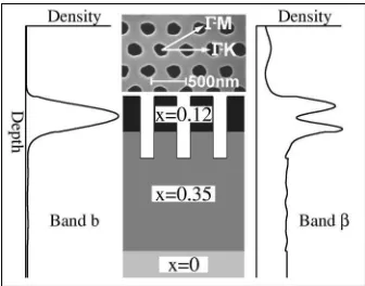
The structure studied is shown in Fig. 1. The waveguide consists of a 400-nm Al0.12Ga0.88As core and a 1.35-mm lower refractive index Al0.35Ga0.65As cladding layer, grown
on a GaAs substrate. The cladding confines the waveguide modes from below, reducing losses due to leakage into the substrate. To pattern the waveguide, triangular lattices of cir-cular holes were defined on a resist mask using electron beam lithography, and fabricated by reactive ion etching. Hole depths of approximately 700 nm were obtained, passing through the core and well into the cladding. This reduces the average index in the cladding in proportion to that in the core, thereby maintaining its effectiveness in confining the modes. Although a range of structures have been fabricated, we concentrate mainly on the results for a lattice period d
5360 nm, with air fill fraction f50.21.
Experimental spectra were obtained using plane parallel white light from a tungsten-halogen lamp, with the reflected
PRB 60
light imaged and projected onto the slits of a grating spec-trometer. The experimental geometry is shown in the inset to Fig. 2. The main part of Fig. 2 shows typical reflectivity spectra, for theG-K lattice direction, at a range of angles of incidence, u. The spectra consist of a smooth background interrupted by sharp resonant features which we interpret as arising from coupling to waveguide photonic band structure modes. As u increases, the energies of these features shift and their strengths and line shapes change markedly. As for shallow gratings,5 the line shapes of the resonances include maxima, minima and dispersive forms.
Theoretical spectra were obtained from a numerical solu-tion to Maxwell’s equasolu-tions for the patterned waveguide structure. To calculate reflectivity spectra, and understand the leaky band structure modes we observe, it is essential that the solution includes the external fields, as well as those within the structure. We have achieved this by developing a scattering matrix treatment which very naturally accounts for the external coupling. This treatment, presented in detail elsewhere,12is a generalization of the text book transfer ma-trix method used for unpatterned multilayer structures.13For a given energy and in-plane wave vector, the
two-dimensional photonic band-structure problem is solved in each patterned layer, to obtain eigenstates of q, the wave-vector component perpendicular to the layer. The scattering matrix for the whole structure is then built up using these solutions, and applying electromagnetic boundary conditions at the interfaces. We solve for the two-dimensional band structures in the individual layers using a plane wave expan-sion within a finite set of reciprocal lattice vectors~RLV’s!. By adopting the scheme of Ho et al.,11 in which the dielec-tric matrix is inverted, rapid convergence is obtained as the number of RLV’s is increased. Our spectra have converged well for calculations using 121 RLV’s, with the energies of the features accurate to within ;1 meV.
Figure 3 shows theoretical spectra for direct comparison with Fig. 2. Both the energies and line shapes of the features below about 1.5 eV are well reproduced. To obtain this agreement, an oxide skin, with refractive index n51.5, was included on the inside surfaces of the holes.6 An oxide fill fraction of 0.15 was used for the core layer and 0.3 for the cladding. The higher oxide value for the cladding is needed to reproduce the experimental featuresa andb. The reason for this lies in the nature of the a andb bands, revealed by comparing the depth dependence of the electromagnetic en-ergy densities for bands b andb, as plotted in Fig. 1. Band b, like most features we observe, is clearly identifiable with the lowest waveguide mode, while the double peak structure of
b ~and a) indicates that it corresponds to a second order waveguide mode.14 Such modes are only well confined, and so observable, if the average refractive index in the cladding is significantly lower than in the guide. In the calculations, this was achieved by assuming increased oxidation of the cladding, to be expected considering its higher Al content. However, we cannot rule out the alternative possibility that the holes are wider at the bottom than the top.
Above 1.5 eV the agreement is less good. There are two likely reasons for this. First, the features in this region are
FIG. 1. Plan-view SEM micrograph and schematic cross section of the patterned AlxGa12xAs waveguide structure. Also plotted are
the in-plane averaged electromagnetic energy densities for bands b andb at 40° incidence in theG-K direction with TM polarization
~see Figs. 2 and 3!.
FIG. 2. Experimental reflectivity spectra, for various angles of incidence, in theG-K direction with TM polarization. The marked features are due to the waveguide bands which are plotted as dis-persions on Fig. 4. The vertical scale bar indicates a change in reflectivity of 0.2. The inset shows the measurement geometry.
[image:3.612.90.258.57.189.2]sensitive to the profile of the holes, which we do not accu-rately know. Second, this spectral region is close to the band gap of the core layer (Eg on Fig. 2!, where strong variation
of the dielectric function will occur. This is not included in the approximation we use for the energy dependence of the refractive indices,15and is likely to lead to significant differ-ences between theory and experiment close to Eg.16
As well as helping to identify the band-structure features, the energy density profiles of Fig. 1 reveal the strong field enhancement which can occur. For band b, the energy den-sity within the guide is;150 times that of the incident light. Correspondingly, the homogeneous line width of the spectral feature is very small:;1 meV in the calculation, reasonably consistent with the experimental value of ;4 meV, which also includes an inhomogeneous contribution. The field en-hancement indicates the potential for nonlinear effects in such structures.
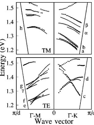
In reflectivity measurements, the angle of incidence, u, determines the in-plane photon wave vector, k5(v/c)sinu. Thus, angular dependent reflectivity spectra can be used to plot out the waveguide photonic band structure. Figure 4 shows dispersions obtained in this way from the experimen-tal and theoretical spectra. The values of k which can be probed are limited to the light cone k<v/c ~the straight diagonal lines on the figure!, but this covers most of the Brillouin zone at the energies of interest. As in Figs. 2 and 3, for the modes with energies ,1.5 eV, the agreement be-tween theory and experiment is very good. Near to Eg, close
agreement is not obtained, as discussed above, and so only experimental dispersions are plotted.
It is instructive to compare the real band structure we determine for the lowest order modes of the waveguide, a-h in Fig. 4, with that expected for an ideal 2D lattice of infinite holes.17 As Fig. 5 shows, the experimental bands look very similar to the 2D calculations, but only when the latter are
[image:4.612.97.250.55.258.2]shifted up in energy by;50 meV. It is also apparent from Fig. 5 that some of the TE polarized bands of the ideal 2D band structure ~solid lines! show up exclusively as TM re-flectivity features ~open circles!, and vice versa. Both this polarization mixing and the energy shifts are accurately re-produced by our waveguide calculations.
The energy shift is due to the waveguide confinement, and it can be modeled, in a very approximate way, by taking the 2D calculations and adding a wave-vector component pendicular to the plane. This model corresponds to a per-fectly confining waveguide, as would be obtained with ideal metal mirrors on either side. Although it gives reasonable energy shifts, the perfect waveguide calculation also predicts large anticrossing gaps of ;70 meV at the c-d, e- f inter-sections. Such gaps are not observed in the real waveguide. It is thus clear that in order to calculate realistic waveguide band structures it is essential to use an approach such as the present scattering matrix treatment, which includes all the layers of the structure.
The polarization mixing, referred to above, is one of the most surprising aspects of our results, and it too is a conse-quence of waveguide confinement. Although symmetry re-quires that all bands in an ideal 2D lattice are pure polariza-tion states,18 in a patterned waveguide, polarization mixing occurs. Overall, the mixing is quite small, but it can have a large effect on the observability of the bands. This is because the folded bands, which consist mainly of high-momentum guided waves, only become leaky, and so appear in the spec-tra, as a result of the low momentum unfolded components mixed into them by the patterning. Indeed, the strength of a spectral feature is determined by the amount of this mixing, which is typically only a few percent. The unfolded states which are involved can, however, be of different polarization to the general character of the band, causing it to appear in the spectra of the opposite polarization.
Having discussed the structure with air fill fraction f
50.21, we make a few remarks about the behavior of other structures with f up to 0.4. Similar bands are seen, but for larger f the band structure shifts to higher energies as the average refractive index is reduced, as shown in the inset to
[image:4.612.358.517.57.170.2]FIG. 4. Experimental~points!and theoretical~lines!dispersions taken from the reflectivity spectra. The upper and lower panels show the features observed for, respectively, TM and TE incident polarizations. The bands labeled a-h correspond to the lowest waveguide mode and can be identified with the 2D bands of Fig. 5. Those labeleda, b, andg correspond to the second order wave-guide mode.
Fig. 3, where the energies of the a and b band at 40° inci-dence are plotted as a function of f. The variation is well described by the theory ~full lines! with the reasonable as-sumption that the oxide thickness remains the same for all fill fractions.
In conclusion, the surface coupling techniques we have presented represent a direct and efficient method to measure photonic band-structure dispersions. We have shown that
sharp resonant features can be accessed directly by angular dependent reflectivity, opening up the prospect of new appli-cations in nonlinear devices, and allowing the possibility of coupling directly to high symmetry points exhibiting heavy photon effects. We have also presented a theoretical treat-ment which provides a precise description of the electromag-netic modes of multilayer photonic band gap waveguides, including their coupling to external fields.
*On leave of absence from the A.F. Ioffe Physico-Technical Insti-tute, St. Petersburg 194021, Russia.
1R. W. Wood, Philos. Mag. 4, 396~1902!.
2R. A. Watts, T. W. Preist, and J. R. Sambles, Phys. Rev. Lett. 79,
3978~1997!; T. Lopez-Rios, D. Mensoza, F. J. Garcia-Vidal, J. Sanchez-Dehesa, and B. Pannetier, ibid. 81, 665~1998!.
3S. C. Kitson, W. L. Barnes, and J. R. Sambles, Phys. Rev. Lett.
77, 2670~1996!.
4T. W. Ebbesen, H. J. Lezec, H. F. Ghaemi, T. Thio, and P. A.
Wolff, Nature~London!391, 667~1998!.
5D. Rosenblatt, A. Sharon, and A. A. Friesem, IEEE J. Quantum
Electron. 33, 2038~1997!, and references therein.
6
T. F. Krauss, R. M. De La Rue, and S. Brand, Nature~London! 383, 699 ~1996!; D. Labilloy, H. Benisty, and C. Weisbuch, Phys. Rev. Lett. 79, 4147~1997!.
7For example, S. Fan, P. R. Villeneuve, J. D. Joannopoulos, and E.
F. Schubert, Phys. Rev. Lett. 78, 3294~1997!.
8N. Akozbek and S. John, Phys. Rev. E 57, 2287~1998!. 9Q. M. Li, C. T. Chan, K. M. Ho, and C. M. Soukoulis, Phys. Rev.
B 53, 15 577~1996!.
10Since this paper was submitted, it has been shown that in-plane
transmission measurements can also yield some dispersion in-formation, from the analysis of finite size effects in lattices con-sisting of just a few rows of holes. See D. Labilloy, H. Benisty, C. Weisbuch, C. J. M. Smith, T. F. Krauss, R. Houdre´, and U. Oesterle, Phys. Rev. B 59, 1649~1999!.
11K. M. Ho, C. T. Chan, and C. M. Soukoulis, Phys. Rev. Lett. 65,
3152~1990!.
12D. M. Whittaker and I. S. Culshaw, Phys. Rev. B 60, 2610
~1999!.
13See, for example, E. Hecht, Optics, 2nd ed. ~Addison-Wesley,
Reading, MA, 1987!, pp. 373–375.
14Note that this is only a qualitative distinction: different
wave-guide modes are in fact mixed by the patterning.
15J. T. Boyd, IEEE J. Quantum Electron. 8, 788~1972!.
16Even a 1% error in the refractive index leads to a significant shift
of;15 meV in the energies of the bands.
17The 2D calculation is based on standard band-structure methods,
for example, Ref. 11, but takes into account the energy depen-dence of the refractive index.
18J. D. Joannopoulos, R. D. Meade, and J. N. Winn, in Photonic