1142 IEEE TRANSACTIONS ON COMPUTER-AIDED DESIGN OF INTEGRATED CIRCUITS AND SYSTEMS, VOL. 23, NO. 7, JULY 2004
[4] IEEE P1500 Standard for Embedded Core Test (SECT) [Online]. Avail-able: http://grouper.ieee.org/groups/1500
[5] M. L. Bushnell and V. D. Agrawal,Essentials of Electronic Testing, for Digital, Memory & Mixed-signal VLSI Circuits. Norwell, MA: Kluwer, 2000.
[6] I. Ghosh, S. Dey, and N. K. Jha, “A fast & low cost testing technique for core-based system-on-chip,” inProc. Design Automation Conf., 1998, pp. 542–547.
[7] I. Ghosh, N. K. Jha, and S. Dey, “A low overhead design for testability & test generation technique for core-based systems,” inProc. IEEE ITC, 1999, pp. 50–59.
[8] M. Nourani and C. Papachristou, “An ILP formulation to optimize test access mechanism in system-on-chip testing,” inProc. IEEE ITC, 2000, pp. 902–1000.
[9] B. Mathewson. Core provider’s test experience. presented at IEEEP1500 Working Group Meeting. [Online]. Available: http:// grouper.ieee.org/groups/1500/pastmeetings.html#dac98
[10] V. Immaneni and S. Raman, “Directaccess testscheme-design of block and core cells for embedded ASICS,” inProc. IEEE ITC, 1990, pp. 488–492.
[11] N. A. Touba and B. Pouya, “Testing embedded cores using partial iso-lation rings,” inProc. IEEE VLSI Test Symp., 1997, pp. 10–16. [12] B. Pouya and N. A. Touba, “Modifying user-defined logic for test access
to embedded cores,” inProc. IEEE ITC, 1997, pp. 60–68.
[13] L. Whetsel, “Core test connectivity communication & control,” inProc. IEEE ITC, 1998, pp. 303–312.
[14] , “An IEEE 1149.1 based test access architecture for IC’s with em-bedded cores,” inProc. IEEE ITC, 1997, pp. 69–78.
[15] D. Bhattacharya, “Hierarchical test access architecture for embedded cores in an integrated circuit,” inProc. IEEE VLSI Test Symp., 1998, pp. 8–14.
[16] P. Varma and S. Bhatia, “A structured test Re-use methodology for core-based system chips,” inProc. IEEE ITC, 1998, pp. 294–302. [17] A. Bensoet al., “HD2BIST: Architectural framework for BIST
sched-uling, data patterns delivering & diagnosis in SoCs,” inProc. IEEE ITC, 2000, pp. 892–901.
[18] E. J. Marinissenet al., “A structured & scalable mechanism for test access to embedded reusable cores,” inProc. IEEE ITC, 1998, pp. 284–293.
[19] M. Benabdenbi and W. Maroufi, “CAS-bus: A scalable and reconfig-urable test access mechanism for systems on a chip,” inProc. IEEE De-sign, Automation, Test Eur., 2000, pp. 141–145.
[20] L. Whetsel, “Addressable test ports, an approach to testing embedded cores,” inProc. IEEE ITC, 1999, pp. 1055–1064.
[21] Z. S. Ebadi and A. Ivanov, “Time domain multiplexed TAM: Imple-mentation and comparison,”Proc. Design, Automation Test Eur., pp. 732–737, 2003.
[22] P. Guerrier and A. Greiner, “A generic architecture for on-chip packet-switched interconnections,” inProc. Design, Automation Test Eur., 2000, pp. 250–256.
[23] W. J. Dally and B. Towless, “Route packets, not wires: On-chip in-terconnection networks,” inProc. Design Automation Conf., 2001, pp. 684–689.
[24] L. Benini and G. De Micheli, “Networks on chips: A new SoC para-digm,”IEEE Comput., vol. 1, pp. 70–78, Jan. 2002.
[25] P. P. Pande, C. Grecu, A. Ivanov, and R. Saleh, “Design of a switch for network on chip applications,” inProc. IEEE Int. Symp. Circuits Syst., 2003, pp. 217–220.
[26] M. Nahvi and A. Ivanov, “A packet switching communication-based test access mechanism for system chips,”Proc. IEEE Eur. Test Workshop, pp. 81–86, 2001.
[27] E. Cotaet al., “The impact of NoC reuse on the testing of core-based systems,” inProc. IEEE VLSI Test Symp., 2003, pp. 128–133. [28] E. H. Volkernik, A. Khoche, J. Rivoir, and K. D. Hilliges, “Modern
test techniques: Tradeoffs, synergies, and scalable benefits,”J. Electron. Test.: Theory Applicat., vol. 19, pp. 125–135, 2003.
[29] M. Nahvi, A. Ivanov, and R. Saleh, “Dedicated autonomous scan-based testing (DAST) for embedded cores,” inProc. IEEE ITC, 2002, pp. 1176–1183.
[30] M. Nahvi and A. Ivanov, “An embedded autonomous scan-based re-sults analyzer (EARA) for SoC cores,”Proc. IEEE VLSI Test Symp., pp. 293–298, 2003.
[31] W. Stallings,Data & Computer Communications, 6th ed. Englewood Cliffs, NJ: Prentice-Hall.
[32] A. Chandra and K. Chakrabarty, “System-on-a-chip test-data compres-sion and decomprescompres-sion architectures based on Golomb codes,”IEEE Trans. Computer-Aided Design, vol. 20, pp. 355–368, Mar. 2001. [33] I. Gosh, N. K. Jha, and S. Dey, “A low overhead design for testability
and test generation technique for core-based systems-on-a-chip,”IEEE Trans. Computer-Aided Design, vol. 18, pp. 1661–1676, Nov. 1999. [34] V. Iyengar and K. Chakrabarty, “System-on-a-chip test scheduling with
precedence relationships, pre-emption, and power constraints,”IEEE Trans. Computer-Aided Design, vol. 21, pp. 1088–1094, Sept. 2002. [35] E. Larsson and Z. Peng, “An integrated system-on-chip test framework,”
inProc. Design, Automation, Test Eur., 2001, pp. 139–144.
[36] Y. Huanget al., “Optimal core wrapper width selection and SOC test scheduling based on 3-D bin packing algorithm,” inProc. ITC, 2002, pp. 74–82.
[37] R. M. Chou, K. K. Saluja, and V. D. Agrawal, “Scheduling tests for VLSI systems under power constraints,”IEEE Trans. VLSI Syst., vol. 5, pp. 175–185, June 1997.
[38] ITC99 Benchmarks. [Online]
[39] ITC’02 SoC Test Benchmarks [Online]. Available: http://www.extra.re-search.philips.com/itc02socbenchm/
Scan Architecture With Mutually Exclusive Scan Segment Activation for Shift- and Capture-Power Reduction
Paul Rosinger, Bashir M. Al-Hashimi, and Nicola Nicolici
Abstract—Power dissipation during scan testing is becoming an im-portant concern as design sizes and gate densities increase. While several approaches have been recently proposed for reducing power dissipation during the shift cycle (minimum-transition don’t care fill, special scan cells, and scan chain partitioning), limited work has been carried out toward reducing the peak power during test response capture and the few existing approaches for reducing capture power rely on complex automatic test pattern generation (ATPG) algorithms. This paper proposes a scan architecture with mutually exclusive scan segment activation which overcomes the shortcomings of previous approaches. The proposed archi-tecture achieves both shift and capture-power reduction with no impact on the performance of the design, and with minimal impact on area and testing time (typically 2%–3%). An algorithmic procedure for assigning flip-flops to scan segments enables reuse of test patterns generated by standard ATPG tools. An implementation of the proposed method had been integrated into an automated design flow using commercial synthesis and simulation tools which was used on a wide range of benchmark designs. Reductions up to 57% in average power, and up to 44% and 34% in peak-power dissipation during shift and capture cycles, respectively, were obtained when using two scan segments. Increasing the number of scan segments to six leads to reductions of 96% and 80% in average power and, respectively, maximum number of simultaneous transitions.
Index Terms—Design for testability, low power, scan testing.
I. INTRODUCTION
Scan architectures represent an attractive solution for both built-in and external testing of digital integrated circuits (ICs). This is because
Manuscriptreceived November 24, 2002; revised February 21, 2003 and June 4, 2003. The work of P. Rosinger and B. M. Al-Hashimi was supported by the Engineering and Physical Sciences Research Council (EPSRC) under Grant GR/S05557. This paper was recommended by Associate Editor K. Chakrabarty. P. Rosinger and B. M. Al-Hashimi are with the Electronic Systems Design Group, Department of Electronics and Computer Science, University of Southampton, Southampton SO17 1BJ, U.K. (e-mail: [email protected]; [email protected]).
N. Nicolici is with the Computer-Aided Design and Test Research Group, Department of Electrical and Computer Engineering, McMaster University, Hamilton, ON L8S 4K1, Canada (e-mail: [email protected]).
Digital Object Identifier 10.1109/TCAD.2004.829797
scan insertion cancels during test the effect of clock gating logic [5]. During scan testing, clock gating logic is disabled and, hence, all flip-flops in the design are clocked in every clock cycle. During normal operation, only the flip-flops which have to be updated are clocked, while all remaining flip-flops are disabled by the clock gating logic. Hence, internal switching activity during testing can exceed the level corresponding to the normal operation of the circuit. Sustained intense switching activity causes overheating and electromigration which can permanently damage the chip under test or seriously affect its relia-bility. Moreover, the effects of parasitic resistance of power supply rails combined with the large current drawn from the power grid by the large number of internal nodes which switch at the same time—re-duce the voltage delivered to cells. Ignoring the effect of this reduction in voltage—referred to as IR (a voltage drop caused by the current flow I passing through the power/ground lines characterised by an electrical resistance R) drop—increases the probability of noise-induced test fail-ures. Fixing IR-drop-related problems requires redesigning the power grid, and hence, a design respin. Given today’s tight market windows and high costs of design respin, it is desirable that such late design fail-ures are preempted if possible from early design stages.
Several methods aiming to solve power-related problems associated with scan-based test have been proposed recently. They fall into the following broad categories.
Low transition test patterns[3], [12], [18]. These methods reduce the number of transitions in the scan-in vectors, and consequently the shift-power component caused by scan-in transitions. These methods have no direct control over the number of transitions in the scan-out vectors, thus, overall reduction in power cannot be guaranteed. More-over, these methods do not address peak-power problems during the capture cycle.
Power conscious ATPG algorithms[13], [14], [19]. These are spe-cial ATPG algorithms which aim to decrease the number of transitions in scan-in and scan-out vectors for shift-power reduction, and also to decrease the Hamming distance between test stimulus vectors and the corresponding test response vectors for capture cycle-power reduction. These ATPG algorithms, while overcoming the shortcomings of min-imum-transition don’t care filling methods, are complex and the gener-ated test sets are generally much larger compared to test sets genergener-ated with regular ATPG algorithms.
Special scan cells[6], [15]. The approach proposed in [6] inserts blocking logic on the outputs of the scan cells in order to block the shift ripple at the inputs of the circuit. Although this method substan-tially reduces power dissipation during the shift cycle, it introduces undesired delay on the data path due to the blocking logic which has a negative impact on circuit’s performance. The work presented in [15] improves the solution from [6] by inserting blocking logic only on the outputs of a limited number of flip-flops which are not on
crit-lation between the flip-flops and activates only one segment in each shift clock. An extra test vector, computed using a special ATPG al-gorithm, is applied during the shift cycle to the primary inputs of the circuit under test in order to further reduce switching due to the shift ripple. A simpler yetvery efficientapproach, firstproposed in [20] and extended later in [16], splits the scan chain into length-balanced segments and enables only one in each shift clock. The maximum number of scan cell outputs which are rippling in each shift clock can be tuned by selecting the appropriate number of scan segments. No blocking logic is inserted on the stimulus path, thus, the perfor-mance of the design is not affected. Moreover, this method reuses test sets generated for standard scan architectures, hence, it does not require special ATPG algorithms. Operating only during shift cycles (which dominate the overall testing time), these methods reduce av-erage power, hence eliminating the risks of overheating and electro-migration. However, in all these approaches, the capture clock is ap-plied simultaneously to all scan cells, leaving the designs prone to noise-induced test failures during capture cycles.
Power dissipation during test capture cycles is likely to be higher than during the functional operation, especially for circuits designed for low power operation. One category of examples are low power finite state machines, where the encodings of “next states” are correlated with the “present states,” such that transitions between pairs of “reachable” states cause low switching activity in the circuit. During test, how-ever, any values can be shifted into the state register, including values corresponding to states unreachable during the normal operation. This breaks the correlation between consecutive values loaded in the state register, and may cause higher switching activity in the circuit. Another category of examples are circuits with clock gating. During the normal operation, the clock gating logic disables a fraction of the flip-flops in the design, thus reducing the maximum number of flip-flop outputs which can change their value. During scan testing, however, the clock gating logic is disabled by test-specific signals. Therefore, all flip-flops in the design are clocked in each test clock, which inherently leads to higher switching activity in the circuit compared to the normal opera-tion mode.
1144 IEEE TRANSACTIONS ON COMPUTER-AIDED DESIGN OF INTEGRATED CIRCUITS AND SYSTEMS, VOL. 23, NO. 7, JULY 2004
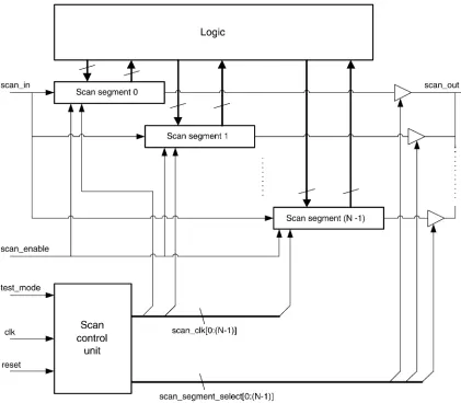
Fig. 1. Scan architecture with mutually exclusive scan segment activation.
both shift and capture power. Basically, the scan chain is split into a given number of length-balanced segments, and only one segment is enabled during each test clock (shift or capture) through the use of a clock gating scheme. Unlike standard scan architectures and previously proposed low power scan architectures [6], [10], [16], [20], which apply the capture clock at the same time to all scan cells, the proposed scan ar-chitecture applies sequentially the capture clocks to the segments of the scan chain. As only a fraction of the flip-flops in the design can change their values simultaneously in each test clock, the proposed architecture reduces not only shift-power dissipation but also capture-power dissi-pation. Hence, this method eliminates the risks of overheating and elec-tromigration as well as the risk of high IR drops during capture cycles which can lead to noise-induced test failures. An algorithmic procedure for assigning flip-flops to scan chain segments enables reuse of test vec-tors generated for single-clock capture. Hence, the proposed low power scan architecture does not require special ATPG algorithms to handle the multiclock capture cycle. Section III presents experimental results on several benchmark circuits.
II. SCANARCHITECTUREWITHMUTUALLYEXCLUSIVESCAN SEGMENTACTIVATION
With the goal of reducing the number of scan cells which are switching simultaneously during testing, the method presented in this paper splits the scan chain into a given number of length-balanced
segments, and enables only one scan segment during each test clock. At each shift clock, a test stimulus bit is shifted into the active scan segment while a test response bit from the previous test pattern is shifted out from the scan segment. Unlike all previously proposed methods based on scan chain partitioning, instead of applying the same single-capture clock to all flip-flops in the design, this scan architec-ture caparchitec-tures the test response for each test pattern over a sequence of clocks cycles, one for each scan segment. Hence, only a fraction (given by the length of the scan segments) of the flip-flops in the design will be clocked in each test clock. This limits the maximum number of flip-flop which can toggle simultaneously, and consequently both shift and capture clock cycles will generate only a limited amount of switching activity in the circuit. This method, replacing standard scan insertion, reduces both average and peak-power dissipation during test. This enables shifting of test data at high frequencies without the risk of overheating the chip under test, and also eliminates the risk of noise-induced test failures, hence avoiding unnecessary respins of the design.
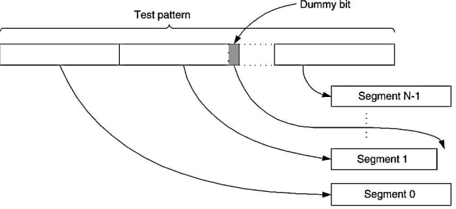
Fig. 2. Compensating length differences among scan segments.
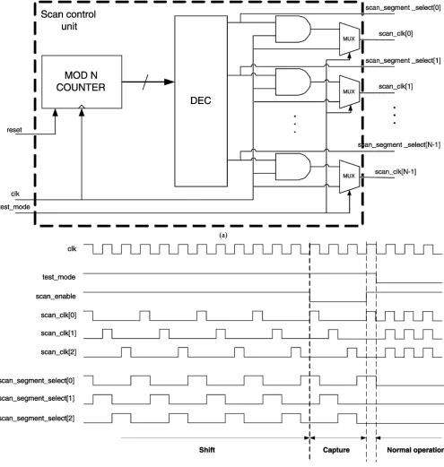
corresponding to the “missing” flip-flops from the shorter scan segments, as shown in Fig. 2. The maximum number of padding bits, i.e.,N 0 1, is much smaller than the length of the scan chain, hence, these extra bits will not affect severely neither the testing time nor the test data storage requirements. All scan segments share the same scan-in (scan in) and scan-enable (scan enable) signals, buteach scan segmenthas a separate clock signal(scan clk[i]; i = 0; N01). The scan segment outputs are connected to the global scan-out line (scan out)through tri-state buffers controlled by mutually exclusive signals (scan segment select[i]; i = 0; N01). Hence, atthe boundaries of the circuit, the low power scan chain appears as a normal scan chain, with standard scan-specific input–output signals (scan in; scan enable and scan out). A scan control unit gener-ates N mutually exclusive clock signals for the N scan segments. A possible implementation of the scan control unit1 is shown in
Fig. 3(a), consists of a moduloNcounter, a decoder and clock gating logic. At each test clock, the active output of the decoder selects the scan segment which will receive the shift or capture clock. Mutually exclusive clock signals(scan clk[0 0 (N01)])for the scan segments are generated by AND-ing the system clock (clk) with the segment selection signals(scan segment select[0 0 (N01)]). The size of the scan control unit depends only on the number of scan segments and, hence, it is not affected by the size of the design.
Fig. 3(b) shows the simulation waveforms for the scan control unit for a low power scan chain architecture with three scan segments. During test mode(test mode = 1), the three clock signals generated for the three scan segments are mutually exclusive during both shift and capture. Initially (t = 0 ns) the scan chain is in shift mode (scan enable = 1). The scan segments are clocked in a cyclic sequence (Segment0, Segment1, Segment2, Segment0, . . .) until all bits of a test pattern are loaded into the scan chain. Att = 360 ns, the test pattern has been fully loaded into the scan chain and the architecture is put into capture mode by asserting low thescan enable signal. Three capture clocks are applied in sequence, one for each scan segment. After the first capture clock(scan clk[0] = 00100), the first third of the circuit response is latched into Segment 0, in the second capture clock(scan clk[1] = 00100), another third of the test response is stored into Segment 1, and in the third and last capture clock(scan clk[2] = 00100), the last part of the circuit response is stored into Segment 2. The multiclock capture cycle is the fundamental
1One possible solution for making the scan control unit testable is to scan its
sequential part, i.e., the flip-flops of the modulo-Ncounter, and add observation points on its outputs (scan clk[0 0 (N01)]andscan segment select[0 0 (N01)]).
difference between this approach and all previously proposed low power scan architectures, which capture the entire test response in a single clock. While in the case of single-clock capture, all flip-flops in the scan chain can change their values simultaneously, the multiclock capture cycle allows at most1=N of the flip-flops in the design to change their value simultaneously. AfterNcapture clocks, the entire test response is available in the scan chain, thus, a new shift cycle can start. During normal operation(test mode = 0), all three clocks are mapped to the system clock. Clock gating circuitry corresponding to the normal operation mode should be built on thescan clksignals and it should be disabled by asserting high thetest modesignal.
As the scan segments are length-balanced and only one scan segment is active during each test clock, the number of simultaneously clocked flip-flops (i.e., the sources of switching activity in the circuit under test) can be tuned at scan insertion by selecting the appropriate number of segments for the scan chain. It should be noted that increasing the number of scan segments also increases the number of capture clocks, and hence, the overall testing time. However, the increase in testing time is insignificant for circuits with long scan chains where the testing time is dominated by the shift cycles. For example, for a circuit with a 1000 flip-flop scan chain, partitioning the scan chain into two segments will reduce the number of simultaneously clocked scan cells to 50% while increasing the length of a test cycle by only one extra capture clock, which represents 0.1% of the original testing time.
concur-1146 IEEE TRANSACTIONS ON COMPUTER-AIDED DESIGN OF INTEGRATED CIRCUITS AND SYSTEMS, VOL. 23, NO. 7, JULY 2004
Fig. 3. Control unit for low power scan chain architectures. (a) Scan control unit. (b) Timing diagram for the scan control unit.
rency at system level for a given power constraint, and hence, to longer test times. Our architecture, however, reduces both shift and capture power, hence enabling increased test concurrency at system level under the given power constraint. Shortening the duration of the stuck-at test session allows more time for the at-speed tests, which can be executed in a more sequential fashion to comply with the given power constraint. It should be noted that the proposed architecture allows at-speed tests to be applied by using the same capture clock for all scan segments. In conclusion, a complete test session will consist of two subsessions: a short and highly parallel test session for stuck faults, when the mutu-ally exclusive clocking scheme is used during both shift and capture,
followed by a low concurrency subsession of at-speed tests, when the mutually exclusive clocking scheme is active only during shift cycles. As testing time represents an inportant factor to the overall cost of test, the proposed scan architecture represents an efficient solution for re-ducing the cost of testing complex chips under power constraints.
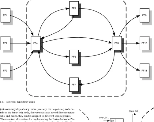
A. Structural Dependencies and Capture Violations
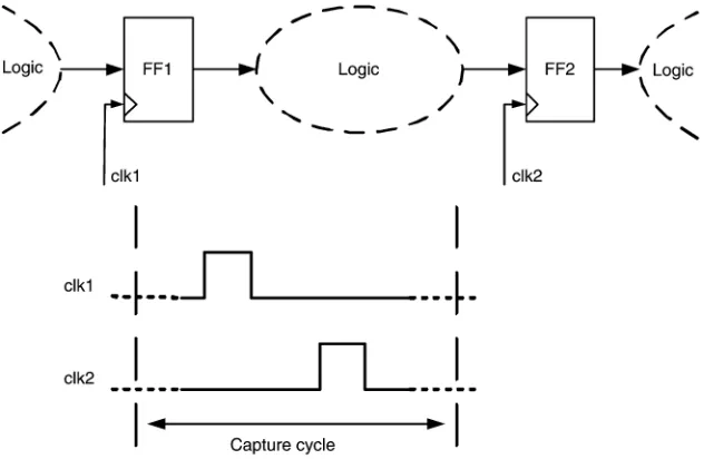
Fig. 4. Capture violation example.
unnecessary. The structural dependencies between the flip-flops in the design are analyzed in the following in order to identify the relevant scenarios. Consider the situation shown in Fig. 4. The test response bit which will be captured in flip-flop FF2 depends on test stimulus bit hold by flip-flop FF1 due to the existing combinational path from FF1 to FF2.
Definition 1: Flip-flop FF2 is said to “depend” on flip-flop FF1 if there is a combinational and/or sequential path from the output of FF1 to the input of FF2.
Definition 2: A test stimulus bit hold by a flip-flop FF is said to be “necessary” if there are other flip-flops in the design which depend on FF and which have not received their capture clocks in the current capture cycle.
According to the timing diagram shown in Fig. 4, FF1 and FF2 are assigned to different scan segments, and hence, their capture clocks do not occur simultaneously. As FF2 depends on FF1, after applying the capture clock to FF1(clk1 = 00100), the value held by FF1, representing stimulus data for FF2, is overwritten with the test response bit.
Definition 3: The situation when a capture clock applied to a flip-flop in the design overwrites a necessary stimulus bit is referred to as a “capture violation.”
The structural dependencies between flip-flops in the design have to be analyzed in order to identify all possible “capture violation” situ-ations. For this purpose, a structural dependency graph (SDG) can be derived from the net list of a design. Each node in the SDG corresponds to a flip-flop in the design, and a directed edge from nodeVito nodeVj means there is a combinational path from the output of flip-flopVito the input of flip-flopVj. According to the SDG model,Videpends on Vj, if there is a path in the SDG fromVjtoVi. In case of a bidirectional dependency between two nodesViandVj, i.e.,ViandVj belong to a cycle in the SDG, flip-flopsViandVj must receive the same capture clock in order to avoid a “capture violation” situation. Generalizing this observation, all nodes from astrongly connected component(or simplystrong component) [7] of the SDG must share the same cap-ture clock, as there is a path between each pair of nodes of a strong component. Consider, for example, the SDG shown in Fig. 5. Nodes FF4, FF5, FF6, FF7, and FF8 form a strong component as there is a path between each ordered pair of them. Applying the capture clock to one of these flip-flops before applying it to the others will result in
a capture violation. For example, capturing first in FF4 will overwrite the test stimulus needed by FF5, FF6, and FF8, and so on. Therefore, flip-flops FF4, FF5, FF6, FF7, and FF8 must be assigned to the same scan segment in order to receive the same capture clock.
From the above discussion, it can be concluded that structural de-pendencies between flip-flops have to be taken into account when as-signing flip-flops to scan segments in order to preserve test stimulus and test response vectors computed for single-clock capture. Section III presents a systematic method for partitioning the flip-flops in the de-sign into equal-length scan segments and scheduling segment capture clocks while avoiding “capture violations.”
B. Scan Chain Partitioning
Partitioning the flip-flops in the design into scan segments must meet the following two constraints.
1) The scan segments have to be length-balanced.
2) There is at least one ordering of the segment capture clocks which does not lead to any “capture violations” between the scan segments.
According to the low power scan architecture presented in Fig. 1, all flip-flops assigned to a scan segment share the same clock signal. As explained earlier, all flip-flops covered by a strong component in the SDG must share the same capture clock in order to avoid “capture violations,” and consequently, they must be all assigned to the same scan segment. This implies that the length of the scan segments will be lower bounded by the size of the largest strong component in SDG. However, the scan segment length is imposed by the given number of scan segment, as the scan segments are length-balanced. It might happen that the size of the largest strong component in the SDG exceeds the scan segment length imposed by the number of scan segments. In this case, it is necessary to “break” the largest strong component into smaller ones, which could be fitted into scan segments of the desired length. “Breaking” a strong component means removing some of the bidirectional dependencies between two or more nodes in the strong component. This can be achieved by replacing a node in the strong componentwith a pair of nodes: aninput-onlynode and anoutput-only
node. This pair will be further referred to as a “extended node.” The
1148 IEEE TRANSACTIONS ON COMPUTER-AIDED DESIGN OF INTEGRATED CIRCUITS AND SYSTEMS, VOL. 23, NO. 7, JULY 2004
Fig. 5. Structural dependency graph.
is justa one-way dependency; more precisely, theoutput-onlynode de-pends on theinput-onlynode, the two nodes can have different capture clocks, and hence, they can be assigned to different scan segments.
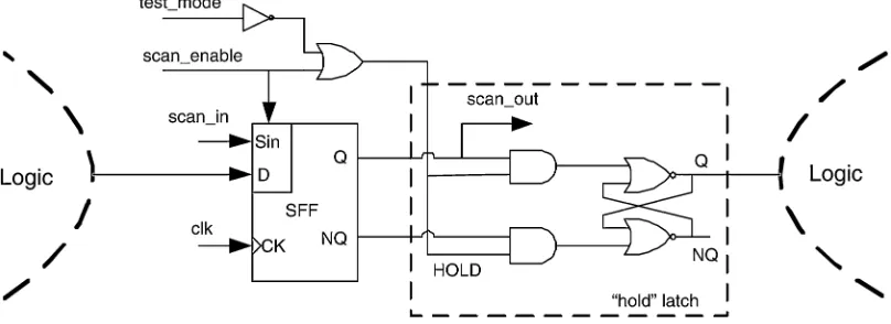
There are two alternatives for implementing the “extended nodes” in hardware. The first possible solution is illustrated in Fig. 6. Flip-flop SFF1 corresponds to a node selected for breaking the largest strong component in the SDG. In this “extended node” implementation, SFF1 is used as aninput-onlynode, and an extra flip-flop SFF2 is added to actas the correspondingoutput-onlynode. In this solution, no extra logic is inserted on the functional data path, thus, the impact on the performance of the original circuit is minimal. The delay introduced by the capacitance of theDinputof SFF2 can be compensated, if neces-sary, by resizing the driving gate. For this implementation of “extended nodes,” the test vectors have to be padded with dummy bits on the posi-tions corresponding tooutput-onlynodes, as these nodes are used only for test response capture.
If the performance of the circuit is not critical, another solution is to implement the pair of nodes using a scan-hold flip-flop [2, p. 483], as shown in Fig. 7. This solution incurs less area overhead compared to the first approach at the cost of an extra delay introduced on the functional data path by the “hold” latch. TheHOLDline of the scan-hold flip-flop is driven by to the scan enable signal. During the shift cycle (scan enable = 1),HOLDis asserted to one and, hence, the “hold” latch is “transparent” to the output value of theDflip-flop. During the capture cycle(scan enable = 0),HOLDbecomes zero, which blocks the stimulus bit into the “hold” latch, while allowing theDflip-flop to capture the test response bit without causing a “capture violation.”
The scan chain partitioning algorithm (Algorithm 1) operates on the SDG derived from the net-list of the design. The algorithm starts by computing the length of the scan segmentsLsegbased on the number of flip-flops in the designNnodesand the given number of scan
seg-Fig. 6. Implementing an “extended node” using an extra scan flip-flop.
Fig. 7. Implementing an “extended node” using a scan-hold flip-flop.
in the SDG have been adjusted according to the segment length, the al-gorithm proceeds to assigning nodes in the SDG to scan segments (line 6). The setof covered nodesCnodesand the first scan segmentSseg0 are initialized to empty sets (lines 6 and 7). An iterative procedure starts to assign flip-flops to scan segments. At each iteration, the algorithm identifies the strong component sc in the SDG which has all fan-out nodes, if any, already covered, i.e., in the covered node setCnodes, and adds the nodes in sc to the current scan segment (line 11). Hence, during the first iterations, the primary outputs of the design, which include also theoutput onlyparts of “extended nodes,” will be assigned to the first scan segmentas they do nothave any fan-outnodes, i.e., no flip-flops in the design depend on them. When the number of nodes in the cur-rent scan segment reaches the scan segment lengthLseg(line 10), the nodes in the current segment are marked as covered and a new empty segment is started. This process is repeated until all nodes in the SDG have been assigned to scan segments. If not all nodes could be fitted into the given number of scan segments (line 13), the algorithm breaks the largest strong component in the SDG and repeats the procedure of assigning strong components to scan segments. The order in which the capture clocks will be applied is the same with the order in which the scan segments were created according to Algorithm 1. This will en-sure that each capture clock will overwrite only stimulus data which became unnecessary for the current capture cycle. The following ex-ample shows how scan chain partitioning works.
Scan Chain Partitioning Algorithm
INPUT:SDG, number of scan segments
OUTPUT:Scan segments as lists of SDG nodes
1 compute , where is the number of nodes in SDG 2 compute
3 compute , where 4 if , then go to line 6 5 break lsc and go to line 2 6
7
8 while , do
9 find ,
where fan-outnode of
10 if , then
11
12 // end while
13 if , then STOP; else goto line 5
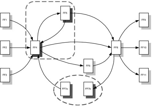
Example 1: Consider the SDG shown in Fig. 5 where nodes FF1, FF2, and FF3 are primary inputs, nodes FF9, FF10, and FF11 are
pri-mary outputs, and nodes FF4, FF5, FF6, and FF7 represent internal flip-flops. The largest strong component in this case contains four nodes, FF4, FF5, FF6, and FF7, as there is a path between each ordered pair of these nodes. Assuming the given number of scan segmentsNsegis four, the scan segment length is three. It can be seen that for the orig-inal SDG, the size of the largest strong component exceeds the scan segmentlength.
The algorithm selects node FF7 as “breaking” node for the largest strong component in SDG. Thus, Node 7 will be replaced with an ex-tended node comprising the pair (FF7a, FF7b) [Fig. 8], where FF7a is theoutput onlynode, while FF7b is theinput onlynode. The largest strong component has now only two nodes, FF4 and FF5, which al-ready complies with the imposed scan segment length. Analysis of the resulting SDG, shown in Fig. 8, shows that flip-flops FF7a, FF4, and FF5, and FF7b, FF6, and FF8, respectively, can be assigned to different scan segments without causing “capture violations,” as long as the first three flip-flops receive the capture clock after the latter three. The scan chain partitioning algorithm continues with assigning nodes to scan segments. As initially the set of covered nodes is empty, the algorithm assigns the three primary output-nodes, FF9, FF10, and FF1, to the first scan segment (Fig. 9). This segment will receive the first capture clock in the multiclock capture cycle as none of the remaining flip-flops in the design depend on the values of the primary outputs, and hence, no “capture violation” can occur. Next, the algorithm assigns nodes FF6, FF7b, and FF8 to the following scan segment as only nodes in Seg-ment0 depend on them, and SegSeg-ment0 has been already scheduled for earlier capture. In a similar fashion, the algorithm assigns nodes FF4, FF5, and FF7a to Segment 2, and nodes FF1, FF2, and FF3, to Seg-ment 3, respectively. From examining Fig. 9, it can be observed that by applying capture clocks to Segment 0, Segment 1, Segment 2, and Segment 3 in this order, no necessary stimulus bits will be overwritten, and hence, no “capture violation” will occur.
III. EXPERIMENTALRESULTS
The efficiency of the low power scan architecture described in Section II was validated by running two sets of experiments using the largest seven ISCAS89 benchmark circuits. Ten additional designs have been generated by concatenating two to seven of the largest ISCAS89 circuits, in order to asses the scalability of the proposed approach to larger designs. The number of flip-flops in the designs considered for experiments ranged from 300 to 7000.
1150 IEEE TRANSACTIONS ON COMPUTER-AIDED DESIGN OF INTEGRATED CIRCUITS AND SYSTEMS, VOL. 23, NO. 7, JULY 2004
Fig. 8. Breaking the largest strong component.
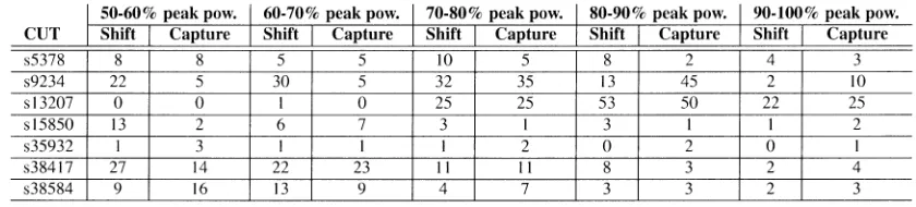
to zeros. Experimental data shows that the fraction of capture clocks for which the power dissipation exceeds 80% of the global peak cap-ture power ranges from 5% (circuit s5378) to 75% ( circuit s13207). Therefore, avoiding capture-power peaks by means of removing the “problem” test patterns from the test set is not feasible for some de-signs without seriously affecting the fault coverage of the test set. De-signs which exhibit high power dissipation during a significant fraction of the capture cycles could benefit from the proposed scan architecture, which reduces both shift and capture power without affecting the fault coverage of the original test set.
The goal of the first set of experiments was to estimate the reduction in average power which can be achieved using the proposed method. Six experiments were performed for each design: one experiment using standard scan chain insertion, and five experiments using the proposed scan architecture with two to six scan segments. The following flow was used in each experiment.
1) Each design was been synthesized using Alcatel MTC35000 technology library.
2) The appropriate type of scan chain (standard or low power) was inserted into the synthesized design.
3) The design was simulated using Mentor Graphics’ ModelSim [8] simulator using five pseudorandomly generated scan patterns in order to capture the toggle activity of internal nodes.
4) The toggle activity was back-annotated to the synthesized de-sign, and an average power estimation was obtained using Syn-opsys’ Power Compiler [17].
Table II shows the relation between the average power dissipation and the number of scan chain partitions. Column 2 corresponds to the
standard single-segment scan chain, while the remaining columns show the results for the proposed low power scan chain architecture using two to six scan segments. For each of the five versions of the low power ar-chitecture, Table II reports the average power dissipation (Pavg) as well as the relative reduction(%red)obtained over the standard scan chain. It should be noted that the reported values correspond to the power dis-sipated by the circuit under test, including the scan chains. The power consumed by the clock tree is not considered. For example, for circuit s38584, the proposed scan architecture with two scan segments reduced the average power by 50% compared to the standard scan architecture. The three scan segment architecture further reduces average power by an additional 42%, which represents 92% reduction compared to the standard scan architecture. The last two rows in Table II show the av-erage and worst case reductions in avav-erage power dissipation.
Table III shows the overhead associated with the proposed low power scan architecture. The increase in testing time due to the multiclock capture cycle can be derived from the number of scan segments and the total number of flip-flops in the design. The number of flip-flops in the original designs is shown in Column 2 (FF). ColumnsxFFshow the number of extended nodes needed to implement the proposed low power scan chain for each experiment. Columns % show the number of extended ondes as a percentage of the total number of flip-flops in the original design. Depending on the solution used to implement extended node, the number of extended nodes represents:
Fig. 9. Scan segments.
TABLE I
FRACTION OFSHIFT–CAPTURECLOCKSCAUSINGHIGHPOWERDISSIPATION
2) The number of scan cells which have to be replaced with scan-hold flip-flops when extended nodes are implemented using scan-hold flip-flops (Fig. 7). It should be noted that, in this case, the total number of scan cells in the design does not increase.
Generally, the percentage of extended nodes decreases and can get as low as zero, as the number of flip-flops in the design increases. This is because, for large designs, the length of the scan segments tend to be much higher than the size of the largest strong component in the SDG and, thus, only few or no extended nodes are necessary during scan chain partitioning. The last two rows in Table III report the average and worst case percentages of extended nodes. Even for the worst case scenarios, reductions up to nearly 70% can be achieved by using the
proposed low power scan architecture at the cost of having at most 12% extended nodes from the total number of flip-flops in the design. The last column in Table III shows the worst case CPU times (in seconds) required to perform the scan chain partitioning algorithm and to insert the resulting scan chain into the designs. The proposed scan chain par-titioning and scan insertion were performed using a tool written in C++ running on a Linux Pentium 4, 1.6 GHz with 512 MB of random access memory.
[image:10.612.85.505.504.599.2]1152 IEEE TRANSACTIONS ON COMPUTER-AIDED DESIGN OF INTEGRATED CIRCUITS AND SYSTEMS, VOL. 23, NO. 7, JULY 2004
TABLE II
AVERAGEPOWERDISSIPATIONVERSUS THENUMBER OFSCANSEGMENTS
TABLE III
[image:11.612.71.515.339.696.2]NUMBER OFEXTENDEDNODESVERSUS THENUMBER OFSCANSEGMENTS
TABLE IV
MAXIMUMNUMBER OFTRANSITIONSPERCLOCK FORATPG-GENERATEDTESTSETS
in each clock cycle was used as a cycle-accurate measure of power dissipation. The six versions of each design (standard scan architec-ture and proposed scan architecarchitec-tures with two to five scan segments) were simulated using 20 linear feedback shift register
the scan control unit was modified for these experiments to apply five consecutive captures, instead of a single one, for each test pattern. Ta-bles IV and V show the peak power values, in terms of number of tran-sitions per clock, for ATPG and LFSR-generated test patterns, respec-tively. Columns 2 and 3 show the peak-power dissipation during shift and capture cycles, respectively. As it can be seen, peak-power dissi-pation during capture cycles is comparable with peak-power dissipa-tion during shift cycles. Thus, reducing peak power in capture cycles is as important as reducing the peak power during shift for avoiding IR-drop related test failures. Columns 4 to 19 in Tables IV and V show the shift and peak power for the proposed scan architecture with two to five scan segments. The %rcolumns show the reductions obtained over the values corresponding to the standard scan architecture. For example, for circuit s38584, the proposed scan architecture with two segments obtained reductions of 21% for ATPG-generated test vectors, and of 27% for pseudorandom vectors in capture peak-power dissipa-tion over the standard scan architecture. Reducdissipa-tions of 26% and 25% in shiftpeak power were obtained for pseudorandom and ATPG-gen-erated vectors, respectively. The last two rows show the average and worst relative reductions for all experiments.
IV. CONCLUSION
This paper presented a scan chain architecture using mutually exclu-sive scan segment activation, where the scan chain is split into length-balanced segments and only one segment is enabled in each test clock (shift or capture). Thus, this architecture is capable not only of reducing average power butitalso eliminates peak-power problems during cap-ture cycles, which have not been addressed by previous approaches based on scan chain partitioning. The maximum number of flip-flops which can change their values simultaneously is limited to the scan segment length. Increasing the number of scan segments reduces the switching activity in the circuit under test and consequently power dis-sipation. The algorithmic procedure proposed for assigning flip-flops to scan segments enables full reuse of test vectors generated using stan-dard ATPG tools without affecting the fault coverage. An implemen-tation of the proposed method had been integrated into an automated design flow using commercial synthesis and simulation tools which was used for a setof experiments performed on 17 benchmark designs. These experiments showed that significant reductions in both peak and average power are achieved when using the proposed scan architecture without affecting the performance of the designs and with minimal im-pact on area and testing time (typically 1%–3%). Hence, this method represents a potential solution to power-related issues associated with scan-based testing.
ACKNOWLEDGMENT
The authors would like to thank the anonymous reviewers for their suggestions which helped improve the quality of the paper.
REFERENCES
[1] Y. Bonhomme, P. Girard, L. Guiller, C. Landrault, and S. Pravos-soudovitch, “A gated clock scheme for low power scan testing of logic IC’s or embedded cores,” inProc. IEEE Asian Test Symp. (ATS), Nov. 2001, pp. 253–258.
[2] M. L. Bushnell and V. D. Agrawal,Essentials of Electronic Testing for Digital, Memory, and Mixed-Signal VLSI Circuits. Norwell, MA: Kluwer, 2000.
[3] A. Chandra and K. Chakrabarty, “A unified approach to reduce SOC test data volume, scan power, and testing time,”IEEE Trans. Computer-Aided Design, vol. 20, pp. 355–368, Mar. 2001.
[4] A. L. Crouch,Design-for-Test for Digital IC’s and Embedded Core Sys-tems. Englewood Cliffs, NJ: Prentice-Hall, 1999.
[5] F. Emnett and M. Biegel, “Power reduction through RTL clock gating,” presented at the Synopsys Users Group (SNUG), San Jose, CA, 2000. [6] S. Gerstendorfer and H. J. Wunderlich, “Minimized power consumption
for scan-based BIST,” inProc. IEEE Int. Test Conf., 1999, pp. 77–84. [7] A. Gibbons,Algorithmic Graph Theory. Cambridge, U.K.: Cambridge
Univ. Press, 1999.
[8] (2000) ModelSim Reference Manual. Mentor Graphics. [Online]. Avail-able: http://www.mentor.com
[9] I. Hamzaoglu and J. H. Patel, “Test set compaction algorithms for combi-national circuits,” inProc. Int. Conf. Computer-Aided Design (ICCAD), Nov. 1998, pp. 283–289.
[10] N. Nicolici and B. M. Al-Hashimi, “Multiple scan chains for power min-imization during test application in sequential circuits,”IEEE Trans. Comput., vol. 51, pp. 721–734, June 2002.
[11] M. Pedram, “Power minimization in IC design: Principles and applica-tions,” inACM Trans. Design Automation Electron. Syst. (TODAES), vol. 1, Jan. 1996, pp. 3–56.
[12] P. M. Rosinger, P. T. Gonciari, B. M. Al-Hashimi, and N. Nicolici, “Simultaneous reduction in volume of test data and power dissipation for systems-on-a-chip,”Electron. Lett., vol. 37, no. 24, pp. 1434–1436, 2001.
[13] R. Sankaralingam, R. R. Oruganti, and N. A. Touba, “Static compaction techniques to control scan vector power dissipation,” inProc. IEEE VLSI Test Symp. (VTS), 2000, pp. 35–40.
[14] R. Sankaralingam and N. A. Touba, “Controlling peak power during scan testing,” inProc. IEEE VLSI Test Symposium (VTS), 2002, pp. 153–159. [15] , “Inserting test points to control peak power during scan testing,” in Proc. IEEE Symp. Defect and Fault Tolerance (DFT), 2002, pp. 138–146.
[16] J. Saxena, K. M. Butler, and L. Whetsel, “An analysis of power reduction techniques in scan testing,” inProc. IEEE Int. Test Conf. (ITC), 2001, pp. 670–677.
[17] (2001) Power Compiler Reference Manual. Synopsys. [Online]. Avail-able: http://www.synopsys.com
[18] S. Wang and S. K. Gupta, “DS-LFSR: A new BIST TPG for low heat dissipation,” inProc. IEEE Int. Test Conf. (ITC), 1997, pp. 848–857. [19] , “ATPG for heat dissipation minimization during test application,”
IEEE Trans. Comput., vol. 47, pp. 256–262, Feb. 1998.