Electrically driven 8-14um band solid-state modulator
C.Y LEE, H.N. RUTT
Optoelectronics Research Centre, University of Southampton, University Road, Southampton, SO17 1BJ, UK
Abstract
Simulation results for an electrically driven 8-14um band, solid-state modulator based on a high purity germanium p-i-n diode are presented. Known carrier recombination mechanisms detrimental to device performance along with ways to reduce their effect are detailed. Device simulations using ‘ATLAS’, indicate that modulation depths of up to 99.5% attenuation for incident infrared radiation centred at 10.6um can be achieved by using ion-implanted device construction and optimisation of the design parameters. Preliminary transient analysis attained higher modulation frequency when transient large bias voltage (2V) is used momentarily during switching.
Keywords: infrared, solid-state modulator, high purity germanium, p-i-n diode
Introduction
The impetus behind this work together with the modulator design criteria, preliminary simulation results and a discussion of modulator performance trade-offs involving wafer thicknesses, dopant doping density and aperture size have been reported previously [1]. In this paper, detailed investigation into various parameters that influence the performance of the modulator such as carrier recombination mechanisms (Auger, Surface and Shockley-Read-Hall) and physical attributes of modulator design (wafer thickness and electrode width) are presented. Optimised device parameters with enhancements from novel use of ion implant processing were then incorporated into the base model and transient analysis was undertaken to evaluate modulation frequency bandwidth.
Modulator design
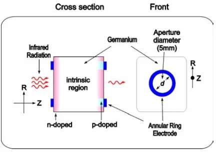
The optimised model used in device simulation is shown in Figure 1. The bulk of the device is ultra high purity intrinsic germanium of the type used to fabricate nuclear radiation detectors. The annular
[image:1.595.311.527.385.538.2]anode and cathode (±Z direction) are ‘n’ and ‘p’ type doped respectively.
Figure 1 : Both cross section and front view of an optimised modulator design shown with
associated cylindrical coordinate orientation (θ
axis omitted).
The doped region decays following a Gaussian distribution profile in the Z direction with its HWHM at a distance of 1.2um. Parameters used in device simulator are listed in Table 1 (a-d)
Carrier properties Values Units
Lifetime 2.5 ms
Electron mobility 3900 cm2/V.s
Hole mobility 1900 cm2/V.s
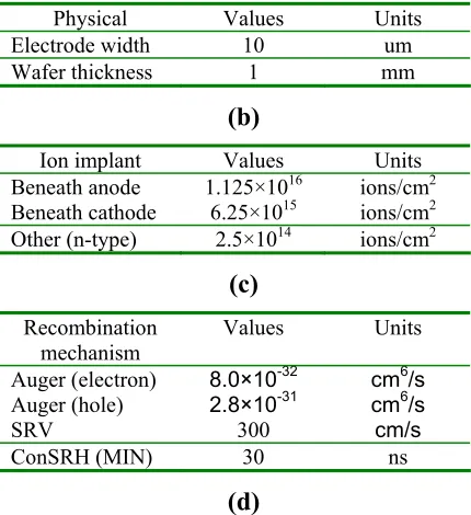
Physical Values Units Electrode width 10 um
Wafer thickness 1 mm (b)
Ion implant Values Units Beneath anode 1.125×10¹⁶ ions/cm2 Beneath cathode 6.25×10¹⁵ ions/cm2 Other (n-type) 2.5×10¹⁴ ions/cm2
(c) Recombination
mechanism Values Units
Auger (electron) 8.0×10⁻³² cm6/s
Auger (hole) 2.8×10⁻³¹ cm6/s
SRV 300 cm/s
ConSRH (MIN) 30 ns
(d)
Table 1 (a-d): Optimised device parameters used in device simulation
The modulator requires 5.6×10¹⁵ holes/cm2
to achieve 95% attenuation in transmitted 10.6um radiation. Attenuation induced during optical “off” or modulator “on” states can be estimated by the following equation:
T
off=
T
0exp(
−
n
p⋅
σ
h)
(1)where T0 is the normalized 100%
transmission, σh is the hole absorption cross
section at 10.6um with a value of 5.33×10 -16 cm2 [8] and n
p is the injected hole area
density given by the following equation:
n
c
x
dx
Z
p
p
(
)
max
0
∫
=
(4)where cp is the hole density (/cm3) profile
through the modulator. The choice for each value listed in Table 1 will be discussed in following sections.
Carrier Recombination
The observed strong 8-14um band absorption in p-type germanium is due to
intervalence band hole transitions between the light hole and heavy hole band [2]. This mechanism is over an order of magnitude greater than the absorption caused by the Drude-Zener free carrier absorption [3]. The previous device used optical injection, whilst this modulator operates on a similar principle by injecting excess carriers into the device electrically. Drift currents through the diode during forward bias introduce carrier concentration gradients that cause transverse diffusion (in the R direction) of carriers in the intrinsic region, inducing IR attenuation. Thus all recombination mechanisms (‘lifetime killers’) detrimental to device performance were thoroughly investigated using the SILVACO ATLAS device simulator. The three main recombination mechanisms can be combined to give an effective bulk recombination lifetime according to the following equation:
−1 −11 −1
+ + =
Auger rad
SRH
r
τ
τ
τ
τ
(1)where
τ
SRH,τ
rad andτ
Auger are theShockley-Read-Hall, radiative and Auger recombination lifetimes respectively and
τ
ris the effective bulk recombination lifetime. Contributions from
τ
Auger andτ
SRH faroutweigh
τ
rad due to germanium’s indirect [image:2.595.66.281.70.305.2]modulator did not suffer performance degradation as the effect is confined to the damaged the regions. The use of HPGe with <1×10¹⁰ ion/cm3 electrically active impurities reduces the SRH recombination rate to just 7.5×10¹⁸ s-1cm3 in the intrinsic region compared to 4.1×10²² s-1cm3 in regions with peak doping density of 9×10¹⁹ ion/cm3. Auger recombination involves the interaction of three particles. Its recombination rate equation can be expressed as:
n3
dt dn =−
γ
(2)
where
γ
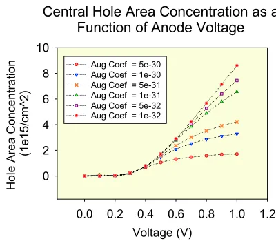
(cm6/s) is the Auger recombination coefficient. When two carriers recombine, the energy released is absorbed by a third carrier (electron or hole). As three particles are involved in Auger recombination, carrier lifetime is inversely proportional to the square of majority carrier density [7]. However, measurement of the precise value is complicated by the presence of SRH and surface recombination (SR). Values ranging from 8×10-32 to 1×10-30 cm6/s have been reported from work spanning the last three decades [9]. Recent publication indicated a better estimate for the hole Auger coefficient to be around 4×10-31 cm6/s instead of the commonly used 2.8×10⁻³¹ cm6/s [11]. We opted for 8×10-32 and 2.8×10⁻³¹ cm6/s for the electron and hole Auger coefficient respectively, a figure widely accepted in the semiconductor industry [10]. The characteristic effect arising from Auger recombination is illustrated in Figure 2. The upper limit of Auger coefficient will severely compromise performance. Auger recombination is an intrinsic property of the material. By reducing the overall carrier density whilst maintaining similar “area” density concentration (i.e. constant hole integral through the device) the effect of Auger recombination can be minimised.Central Hole Area Concentration as a Function of Anode Voltage
Voltage (V)
0.0 0.2 0.4 0.6 0.8 1.0 1.2
Hole Area Concen
tr
a
tio
n
(1e15/cm^2)
0 2 4 6 8 10
[image:3.595.309.509.69.244.2]Aug Coef = 5e-30 Aug Coef = 1e-30 Aug Coef = 5e-31 Aug Coef = 1e-31 Aug Coef = 5e-32 Aug Coef = 1e-32
Figure 2 : The hole area concentration
integrated through the modulator in the middle of the aperture for different Auger coefficients (AC). The characteristic effect of Auger recombination is clearly seen; when the Auger Coefficients is high the hole area density saturates at high forward voltage.
Transmission for different wafer thickness
-20.00 0.00 20.00 40.00 60.00 80.00 100.00 120.00
0.00 0.50 1.00 1.50 2.00 2.50 3.00
Current (A)
Tran
smissio
n
(
%
)
1mm 2mm 3mm
Figure 3 : Improved attenuation using thicker wafers
This can be done by using thicker wafers to allow spread of carriers in the Z direction in the intrinsic region. However, to maintain reasonably low device voltage drop and near constant Z direction carrier concentrations, the device thickness must be less than the diffusion length (Ld). Ld can
be estimated using the following equation:
L
d=
D
aτ
bulk (5)where Da is the ambipolar diffusion
coefficient at 66.03 cm2s-1. Assuming
τ
bulk [image:3.595.314.526.363.487.2]magnitude higher compared to SRH recombination provided SRH is kept low by using HPGe. Recombination in the intrinsic region is illustrated in Figure 4.
Recombination Rate Comparison
1E+18 1E+19 1E+20 1E+21 1E+22
1.00 10.00 100.00 1000.00
Distance through Diode (um)
R
a
te
(
car
ri
er
s/
scm
^3)
[image:4.595.74.275.139.261.2]SRH Recom Rate Auger Recom Rate
Figure 4 : Recombination rate calculated in the intrinsic region, in the middle of the aperture at 0.525 (V). Auger recombination dominates..
Surface recombination
The effective carrier lifetime is defined as follows:
surface bulk
effective τ τ
τ 1 1
1 = + (6)
τ
surface is dependant on the surfacerecombination velocity (SRV) which is conventionally treated as a diffusion process normal to the surface (along the Z-direction) [7]. Modelling SRV is important as the rate at which carriers recombine at the surface may exceed that of bulk recombination if a large density of energy states is present at the surface causing
τ
bulk>τ
surface. As an example of its effect on thedevice, an increase of SRV from 300 cms-1 to 1000 cms-1 will reduce the modulation depth from 95% to 60% attenuation. Etched germanium wafers commonly achieve SRV values of 100cms-1 [12]. However, SRV
values increase with time and experiments conducted showed that a stable 300 cms-1 SRV is attainable using CP4A acid etch [9]. As maintenance of low SRV through multiple process steps including optical coating may prove difficult we investigated an alternative solution. By using a low dose ion implant over the full aperture of the
device the surface potential is raised which reduces the effective SRV (i.e. lower probability for carriers to recombine at the surface).
Transmission as a function of Implanted ions
0.0000 20.0000 40.0000 60.0000 80.0000 100.0000 120.0000
0.00 0.50 1.00 1.50 2.00 2.50 3.00
Current (A)
Tr
ansm
issio
n
(
%
[image:4.595.312.516.149.267.2]) 1e11/cm2 ion dose 1e13/cm2 ion dose 1e14/cm2 ion dose
Figure 5 : Increased depth of modulation using low dosed, ‘n’ type, area ion implant in regions surrounding electrodes (R direction).
Low dose area ion implant performed extremely well especially when high SRV values are present. Figure 5 depicts the performance of the modulator with an SRV value of 1000 cm/s.
[image:4.595.310.547.445.601.2]Electrode Width
Figure 6 : Power required to achieve 95% attenuation in transmission for different electrode width
Smaller electrode widths showed a substantial reduction in the power needed to achieve similar attenuation as shown in figure 6. This is due to the reduction in redundant drift current through the device
Effects of Varying Electrode Width
1.0000 1.5000 2.0000 2.5000 3.0000 3.5000 4.0000 4.5000 5.0000
0.0000 50.0000 100.0000 150.0000 200.0000 250.0000
Electrode Width (um)
No
d
e
Cu
rr
e
n
t
(A
)
0.0000 0.5000 1.0000 1.5000 2.0000 2.5000 3.0000
Pow
e
r (
W
)
which does not contribute to its performance. Electrode widths of ≥10um were used in the device modelling as it reflects the limitations in device fabrication capabilities available to us.
Modulation frequency: Transient analysis
Transient analysis allowed investigation of modulator switching frequency capability. Using optimised device parameters listed in Table 1 (a-d), the diode was driven with a bias voltage of ±2 (V) for 10us (device dependant values) transiently after switching. This was intended to enhance the rate of carrier injection and extraction of the stored charge. Through this method, the carrier equilibrium concentration time required to reach the modulator “on” state is reduced from 940us to 870us as the steady state drift current is established much faster. Modulation frequency increased by 90 Hz using this method. The current through the diode showed oscillatory behaviour before stabilizing at 2.7 A. The peak current reached during oscillation is at 6 (A). This behaviour is not understood at present time, and may be a numerical artefact.
Conclusion
We have established a comprehensive model of the operation of an electrically operated germanium infrared modulator. The device shows a strong sensitivity to the poorly known Auger coefficient, but this effect can be mitigated by using thicker substrates. The deleterious effects of surface recombination can be efficiently suppressed using low dose area implants. Narrow electrodes give considerable reductions in required operating power and current. Time dependent simulations indicate that whilst transient forward over-voltages and pulsed reverse bias increase the speed of operation, unexpected oscillatory currents are predicted, which
require further investigation. Efforts are currently in hand to fabricate a demonstration device.
References
1. Suresh Uppal, Harvey N. Rutt, Paper A1, 2nd EMRS-DTC Technical Conference, Edinburgh, 2005
2. Fairley, P. D. (2000). J. Phys. D: Appl. Phys. 33 2837-2852
3. Kahn A H 1955, Phys. Rev. 97 1647-52 4. Landsberg P T 1991 Recombination in
Semiconductors (Cambridge University Press)
5. Bridgers H E, Staff J H and Shive J N (ed) 1958 Transistor Technology vol 1 (Princeton, NJ: Van Nostrand-Reinhold) 6. F.E. Roberts, Solid-state electronics, 1961, Vol.2, No.1, pp.8-13, Pergamon Press
7. Sze S M 1985 Semiconductor Devices: Physics and Technology (New York: Wiley)
8. Capron E D and Brill 0 L 1973, Appl. Opt. 12 569-72
9. Fairley PD, 2000, PhD Thesis, University of Southampton
10.D.K. Schroder, Semiconductor Material and Device Characterization, 2nd Edition, Wiley, NewYork, 1998, pp. 424–425.
11. D.Poelman, P. Clauws, B. Depuydt, Solar energy materials and solar cells 76 (2003) 167–173
12. Hannay N B 1960 Semiconductors 2nd edn (Reinhold)
Acknowledgements