O R I G I N A L A R T I C L E
Finite element modeling on the effect of intra-granular porosity
on the dielectric properties of BaTiO
3
MLCCs
Graham Dale
1|
Maureen Strawhorne
1|
Derek C. Sinclair
2|
Julian S. Dean
21AVX Ltd, Coleraine, County
Londonderry, UK
2Department of Material Science &
Engineering, University of Sheffield, Sheffield, UK
Correspondence
Julian S. Dean, Department of Material Science & Engineering, University of Sheffield, Sheffield, UK.
Email: [email protected]
Funding information
Engineering and Physical Sciences Research Council, Grant/Award Number: EP/L017563/1, EP/P019919/1
Abstract
The effect of porosity on the electrical properties of BaTiO3-based Multilayer
Ceramic Capacitors (MLCCs) is studied. A dense ceramic prepared via powder from a solid-state processing route is compared against a ceramic that contains intra-granular pores from powder prepared via hydrothermal processing. Finite element models are created to contain intra-granular pores, solved and analyzed to show an increase in the electric field and current density surrounding the pores. For single-pore and two intra-pore arrangements, the electric field is enhanced by a factor of~1.5 and 2.5, respectively, when compared to a fully dense (pore-free) material. For ceramics with equivalent density, the number of pores dramatically alters the electrical response. For a system containing 100 pores, the electric field can increase at least fourfold, therefore facilitating a possible starting route for electrical breakdown of the grain. These results are compared to the Gerson-Mar-shall model, typically used in the literature for the calculation of the breakdown strength due to porosity. The results highlight the need to include the effect of adjacent pore interactions. Although studied here for BaTiO3-based MLCC’s the
results are applicable to other devices based on ceramics containing porosity.
K E Y W O R D S
barium titanate, degradation, finite element analysis, multilayer capacitors, pores/porosity
1
|
INTRODUCTION
There are over 2 trillion BaTiO3-based multilayer ceramic
capacitors (MLCCs) produced every year for a variety of applications. Despite this staggering number of compo-nents, the electronics market constantly demands higher capacitance and therefore thinner dielectric layered BaTiO3-based MLCCs for applications (e.g., automotive)
that require device reliability at increasingly higher operat-ing temperatures (e.g., >125°C) and voltages (e.g.,>25 V). To meet this demand, the thickness of the dielectric layers in MLCCs have been reduced to below 1 micron and the
electrical response of the ceramic layers is therefore depen-dent on only a few grains of BaTiO3-based material
between each set of internal electrodes. This has been achieved by a combination of using nano-sized starting powders and innovative processing methods. As a conse-quence, each dielectric layer in an MLCC is exposed to significant dc electric fields and this can lead to fatigue, degradation and ultimately, dielectric breakdown. The elec-trical response(s) of the dielectric layers is highly depen-dent on any changes and/or variability in the ceramic microstructure of the dielectric layers and is therefore inti-mately linked to the starting powders and processing
-This is an open access article under the terms of the Creative Commons Attribution License, which permits use, distribution and reproduction in any medium, provided the original work is properly cited.
©2017 The AuthorsJournal of the American Ceramic Societypublished by Wiley Periodicals, Inc. on behalf of American Ceramic Society (ACERS)
ally attributed to various types of defects, generally arising from the quality of the starting powders and the processing route(s).1 For example, the breakdown strength typically decreases with increased porosity and grain size2-5
One of the widely accepted models relating the effects of porosity on the breakdown strength of porous ceramics is the Gerson-Marshall model,3 where the dielectric strength in porous ceramics is dependent on the porosity and grain size. This model predicts how the breakdown strength of the material decreases from a fully dense bulk value, when porosity is introduced. Both experimental results and theoretical calculations reveal the breakdown strength of ceramics can be reduced by a factor of ~2 if the porosity reaches 10%. A key feature of this model is that the only significant parameter is the number and size of the pores parallel to the applied voltage; however, it does not consider their proximity and interactions in other directions.
Traditionally, BT is prepared by a solid-state (SS) reac-tion that involves ball milling of BaCO3 and TiO2.6 The
mixture is then calcined at high temperature. BT powders prepared via this solid-state route (SS-BT) can be highly agglomerated, with a large average particle size and can contain high impurity contents due to inherent problems such as high reaction temperature and heterogeneous solid phase reaction.7-9 These have been identified in creating poor electrical properties of sintered SS-BT ceramics; how-ever, processing routes have been substantially improved and it is now possible to fabricate, nano-sized SS-BT pow-ders that are suitable for obtaining high quality, dense SS-BT ceramics.
To eliminate many of the early problems associated with SS-BT powders, a variety of wet chemical synthesis routes have been developed to generate higher purity, homogeneous, reactive ultrafine barium titanate powder at lower temperatures. Aqueous-based Hydrothermal (HT) processing is of great interest because of the possibility of producing highly crystallized, well-dispersed and sintering-active nano-powders at low temperatures.10-14Despite these apparent advantages, HT-BT powders can suffer from the presence of structural water during fabrication that can gen-erate significant levels of intra-granular porosity.12-14 For
powders are heated above ~700°C,14 therefore creating intra-granular pores in the grains of sintered HT-BT ceram-ics.
Here, we use a combination of finite element modeling (FEM) and experimental results from sets of MLCCs fabri-cated from both HT- and SS-BT powders to elucidate the influence of intra-granular porosity on the electrical proper-ties of these devices.
2
|
EXPERIMENTAL METHODOLOGY
AND RESULTS
Two different BT-based MLCCs have been fabricated and analyzed at AVX (Coleraine). Two lots of MLCCs with dimensions of 0.3090.15 mm were fabricated, each with 4.6 micron dielectric layers. Lot A was fabricated using a SS-BT source powder while Lot B was based on a HT-BT source powder. Simultaneous incorporation of minor dopants and additives were employed to achieve X7R capacitor temperature stability (TCC). The MLCCs used 230 electrodes and fired at temperatures exceeding 1200°C, in a reducing atmosphere typically controlled by H2, N2,
O2and H2O, (log10 pO2(atm)~ 16 to 19). The ceramic
microstructure of the dielectric layers in the MLCCs were studied by scanning electron microscopy (SEM) using a MIRA3, TESCAN. A highly accelerated life-test (HALT) method was employed to establish life reliability for both lots, all measured to failure. Each lot tested over 30 MLCCs using a voltage of 142 V applied at an elevated temperature of 150°C.
Three types of intra-granular pores are observed in Fig-ure 1B. Type, (i) where a single grain contains one large pore. The location of this can vary and in some cases may be located towards the edge of the grain surface. These sin-gle pores generally appear to be large, taking up a signifi-cant fraction of the grain volume. Type (ii) show that two pores can be created that are close together, while the dis-tance and orientation between these two pores, in relation to the placement of the electrode, varies. Finally type (iii) highlights where a grain contains many smaller intra-granu-lar pores. These appear to be smaller pores but are dis-tributed throughout the grain.
The implications of these intra-grain pores for indus-trial applications can be highlighted when the lifetime of MLCC components are fabricated from layers of these materials. Figure 2A shows a typical resistance-time HALT profile for a single MLCC from each set. In this case, the HT-BT based device has a higher initial resis-tance of ~4 MΩ but it quickly drops and fails approxi-mately 6 hours into the test. The SS-BT based component has a different profile, starting with a lower resistance of ~2.2 MΩ but with a marked increase in lifetime to over 16 hours. As the resistance falls to zero, the lifetime of the component is recorded. As shown in Figure 2B this can vary, however, typically the SS-BT leads to a greater lifetime when compared to the HT-BT based MLCC. Although both profiles are reasonably sim-ilar, the slope of the cumulative failures is rather differ-ent and therefore suggests the origin of breakdown is different in both cases. Understanding the role of intra-granular porosity in the dielectric layers on the failure of
an MLCC is therefore critical in understanding how components behave and how to achieve improvements to enhance device lifetime.
F I G U R E 1 SEM images of (A)
solid-state and (B) hydrothermal-based BaTiO3
ceramic as part of a layer within an X7R MLCC. A selection of hydrothermal grains is annotated for clarity to show different features within single grains; (i) a large, single granular pore; (ii) two intra-granular pores; and (iii) multiple smaller pores
F I G U R E 2 Typical time-dependent resistance profiles for both materials based on an accelerated lifetime test (HALT) conducted
using 142 V at 150°C. (A) shows a typical resistance profile
Gmsh18 and solved using Elcer. These different regions possess an individual conductivity (r) and relative permit-tivity (er) simulating an electrical heterogeneity within the
model without the need for equivalent circuits and constant phase elements.
We simplify the model to study the effect of pores on the HT material by studying the response of an individual grain. We assume a cubic grain of 1lm3 where the pores are located internally as spherical objects. The center of the cube is set as the origin and the cube extends from 0.5-0.5lm along each axis. A constant potential difference of 142 V is applied across the top and bottom surfaces of the grain, aligned to thez-axis, thus simulating the HALT con-ditions. The response of the system is taken once the cur-rent flow reaches a static equilibrium. We apply material properties of r= 2.59 10 8Sm 1 and er = 3681 that
replicate the HT-BT ceramic at 150°C (with no dc bias) as measured from a combination of impedance spectroscopy and fixed frequency permittivity measurements (data not shown). The pore is assigned the properties of typical air19 withr =0.5 910 14 Sm 1and er = 1.
A single 1lm3 HT-grain using these properties gener-ates a resistance of 40 TΩ and an internal uniform electric field of 142 MVm 1when a potential difference of 142 V is applied across the contacts. To provide comparison to other geometry and material properties, the results are
reduction in grain density to 50.7%.
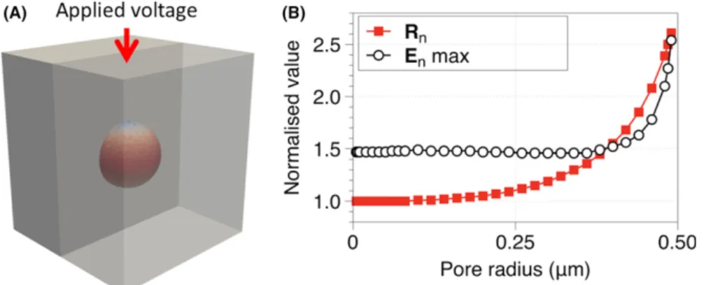
The normalized grain resistance (Rn) and maximum
electric field (En,max) both increase with the pore size,
Figure 3B. The existence of the smallest pore generated (5 nm) initially generates an increased En,max within the
pore of a factor of 1.5. As the pore size increases En,max
remains relatively constant at 1.5 until the pore radius increases to 0.5lm (equivalent to a 52% dense grain) where it dramatically rises to a factor of 2.5 and beyond.
Rnrises by a similar factor as the volume of the pore rises
to 50% of the total volume (representing a 52% dense grain). At small pore sizes, however, less than 5% of the grain volume, no resistance change is detectable.
In addition to assessing the extrinsic electric proper-ties associated with incorporation of pores, Elcer also allows the internal electrical microstructure to be probed. Figure 4A-C show a central cut through pores of radius 0.1, 0.2, and 0.48lm, respectively, and are displayed with a color coding for the electric field profile. A streamline analysis is overlaid on the model to highlight the direction and intensity of the electric field vector. Where lines are close, the field is constricted and there-fore generates inhomogeneous electrical behavior. The stream trace is found to be similar for both the current density and electric field profiles but highlights different phenomena.
F I G U R E 3 (A) A slice through a 3D model representing a single intra-granular pore of radius 0.10lm inside a 1lm3grain giving rise to a
grain density of 96.6%; (B) the normalized maximum electric field factor (En,max) and normalized resistance (Rn) as a function of pore radius.
For a pore radius of 0.10lm (grain density 99.6%), shown in Figure 4A, the field flows around the pore avoid-ing the resistive path through it, as shown by the near zero current density inside the pore. There is an increased flow of current around this region, increasing to a factor of 1.5. This also generates a reduction in the electric field, above and below the pore in the direction of the applied voltage as shown along the z-axis in Figure 4D. Of greater signifi-cance is the increase in electric field around the sides of the pore by a factor of 1.5 perpendicular to the current flow, as shown in Figure 4D. This increased electric field remains relatively constant as the pore size increases until the pore begins to interact with the sides of the grain. At this point, the surface of the box and the pores surface begin to interact causing the current to be squeezed through the narrow region between the pore and grain surfaces. This creates a constriction resistance, increasing the resis-tance of the system by over twice that of the unrestricted case shown in Figure 4I. A similar increase in the electric field is also created in Figure 4C,F.
3.2
|
Interacting pores
Experimentally, whilst some grains possess a single internal pore, there are many grains where two or more pores are located close together. To simulate how these interact, we fix a pore radius of 0.10lm and align two intra-granular pores such that their centers are positioned either along an axis perpendic-ular (Figure 5) or parallel (Figure 6) to the applied voltage along the z-axis. We create a set of models altering the distance between them from 0.01 to 0.30 lm ensuring the pores do not interact with the surface of the grain. This is to ensure the effects observed arise only from the pore-pore interaction.
If the pores are located perpendicular to the field, the current is forced around them as shown in Figure 5A-C. This can dramatically increase the electric field by a factor of 2.5, when they are close together as in Figure 5D. This is due to some of the current being directed and squeezed between the two pores. An associated constriction resis-tance is also observed in Figure 5G with an observed spike in the current density between the pores.
F I G U R E 4 The size effect of a single intra-granular pore on the normalized electric field (En) and current density (Jn) profiles for a pore
radius of 0.10 (A, D, G), 0.20 (B, E, H) and 0.48lm (C, F, I) giving rise to grain densities of 99.6%, 96.6% and 53.7%, respectively. Parts
(A-C) show a central 2D slice through the solved 3D model and highlight a stream trace and color of the electric field generated where red and blue
indicate high and low fields, respectively. Parts (D-F) and (G-I) showEnandJnthrough the centre of the pore for the various radii. These are
If the pores are orientated parallel to the field the behav-ior is different. If they are close together the current cannot flow between them and they effectively act as a single large pore, shown in Figure 6D,G, and are comparable with the field profiles in Figure 4. The electric field between them is reduced almost to zero. As seen from the current density profiles, the width of the reduced current density is also different along the two directions. Along the
x-axis the width of the pores is similar to that of an indi-vidual pore, whereas in thez-axis it extends twice as much. This indicates a stagnation point in the field flow arising due to one pore shielding the response of the other. The effective size of the combined pores in the current direction is thus dependent upon the pore profile along the z-axis, consistent with the Gerson-Marshall model.3
As the pores separate, they begin to act independently again, behaving as two single pores, Figure 6C. An associ-ated increase in current density and electric field is observed between them converging towards unity.
These two orientations are compared in Figure 7. Here, the normalized electric field generated by these models is plotted as a function of the distance between the pores. At approxi-mately 0.40lm, four times the pore radius, the electric field returns to unity, indicating that the pores can once again be
treated as non-interacting defects. This trend is also observed for the current density and for other pore sizes (not shown).
Experimentally, there appears no trend to the orientation of the pores in the grain with respect to the applied volt-age, Figure 1. To study what affect this may have, we con-tinue with two pores of radius 0.10lm but set at a fixed center-to-center distance apart of 0.15lm. This provides a factor of 1.3 that allows us to observe the effect as a func-tion of pore orientafunc-tion. As shown in Figure 8A we start with the angle between both pores of 0°, aligning the pores perpendicular to the applied voltage as shown in Fig-ure 8B. They are then rotated around their centre to an angle of 90°, aligning the pores parallel to the applied volt-age as shown in Figure 8E.
At 0°, we observe the typical constriction and an associ-ated increase in the electric field by a factor of 1.3. As they rotate, this reduces quickly to less than a factor of 1.1 at 40°with the corresponding model shown in Figure 8D. At this point, the pores begin to generate a “shielding”effect that reduces the constriction factor back to unity as the cur-rent flows around both of them and they now begin to act as a single, larger pore. Thus, orientation of the pores with respect to the applied voltage is a significant factor in cera-mic cera-microstructures.
F I G U R E 5 The effect of distance on the normalized electric field (En) and current density (Jn) profiles for two perpendicular intra-granular
pores with respect to the applied voltage. The profiles are shown for a pore of radius 0.10lm, with a distance between the pores of 0.01 (A, D,
G) 0.10 (B, E, H) and 0.20lm (C, F, I). Parts (A-C), (D-F), and (G-I) show a central 2D slice through the various distances, with an overlaid
stream trace. The electric field colour of red and blue indicate high and low fields, respectively. The fields are measured both parallel and
3.3
|
Multiple pores
The maximum electric field generated from systems with intra-granular pores can vary dramatically depending on its location, size, and distance to neighboring pores. Experi-mentally there can be a mixture of grains in a dielectric
based on those without pores to those with single pores, a few pores or many small pores, Figure 1B.
As shown for the single and double interacting pore case scenarios, the increase in electric field can be signifi-cant and as such we use our FEM to understand its possi-ble significance for multi-pore systems. Each model has a fixed overall density but the number of pores present is varied. We randomly place the pores into the grain, treating them as hard spheres to avoid any overlap. This is shown in Figure 9A for an 85% dense grain with 100 identical pores. Due to the large variation in configurational posi-tions, we run 100 random configurations and average the results. When many pores are present in a grain, there is a significant chance that some pores are very close together in different orientations, as shown in Figure 9B which is taken from a slice of Figure 9A. This one slice contains many pores that appear not to be interacting but two regions are highlighted for interest. Near the top left (i), two pores have a highly elevated electric field and a large electric field is generated in the model. This arises as the two pores are close together, parallel to the applied voltage, causing a high constriction resistance between them. Located at the bottom left (ii) are two pores close together
F I G U R E 6 The effect of distance on the normalized electric field (En) and current density (Jn) profiles for two parallel intra-granular pores
with respect to the applied voltage. The profiles are shown for a pore of radius 0.10lm, with a distance between the pores of 0.01 (A, D, G)
0.10 (B, E, H) and 0.20lm (C, F, I). Parts (A-C), (D-F), and (G-I) show a central 2D slice through the various distances, with an overlaid
stream trace. The electric field colour of red and blue indicate high and low fields, respectively. The fields are measured both parallel and
perpendicular to the applied voltage,z- andx-axes, respectively
F I G U R E 7 The effect of the normalized electric between the pores as a function of the distance between them and their
orientation. A convergence towards the value of a homogenous grain
is observed at approximately 0.4lm in both cases, approximately
but due to their orientation they have a reduced electric field between them.
As the grain density increases (i.e., the total volume fraction of pores decreases) the average electric field in the grain decreases, Figure 9C. Of more significance is the increase in electric field with an increasing number of pores for a fixed grain density, Figure 9C. This suggests (for a fixed grain density) that a reduction in the break-down strength in a ceramic is more likely to occur where there is a large number of intra-granular pores.
To highlight the significance of pore interactions revealed by our FEM model we compare this to the Gerson-Marshall model3 (where pore interactions are not considered) to esti-mate the normalized breakdown strength reduction that arises from changes in porosity and pore-size. To provide a better comparison to the FEM model, we assume the breakdown
strength of the material is set as unity for a fully dense sam-ple. This allows us to create a prediction from the FEM of the normalized breakdown strength. Both models have been tested for set densities of 85%, 90% and 95% and both show the density significantly influences the breakdown strength, Figure 10. For a small number of pores, the Gerson-Marshall model shows a reduction in the normalized breakdown strength from~0.65 for 5% porosity to<0.5 for 15% porosity, Figure 10A. However, if the pore size is decreased (therefore increasing the number of pores forming the porosity) the nor-malized breakdown strength appears to partially recover and increase to~0.7 and ~0.5 for 5% and 15% porosity, respec-tively, Figure 10A. This is due to the underlying assumption in the model that breakdown will occur along a purely paral-lel pathway (i.e., column) in the direction of the applied volt-age that contains the maximum number of pores and therefore a minimum amount of ceramic material. There is no consideration of pore interactions along the perpendicular directions and/or between adjacent “columns”. As the pore size decreases, the probability of a large number of pores located in any one parallel column decreases and therefore the breakdown strength partly recovers.
For the FEM model a similar trend in the reduction in normalized breakdown strength with decreasing grain den-sity is observed for a few pores; however, in contrast to
F I G U R E 8 The effect of Enverses orientation for two
intra-granular pores of radius 0.10lm in single grain, set at a distance of
0.10lm apart. Their orientation is rotated from orthogonal to the
applied voltage at angles of (B) 0°, (C) 20°, (D) 45°, and (E) 90°. A
stream trace and colour of the electric field is overlaid where red and blue indicate high and low fields, respectively
F I G U R E 9 A multi-intra-granular model that ranges from containing a single large pore to 100 small pores. The size of the pore is controlled to achieve a specific grain density. Part (A) a slice of an 85% dense grain with 100 pores with (B) showing a 2D slice of
En, highlighting how the orientation of the pores can lead to high and
low electric fields. Part (C) the average normalized electric field (En,
the Gerson-Marshall model, the normalized breakdown strength for a fixed grain density decreases with an increas-ing number of pores, Figure 10B. For all three grain densi-ties, the normalized breakdown strength decreases significantly to a final value of ~0.28-0.35, Figure 10B. This trend occurs due to enhanced electric fields occurring between adjacent interacting pores.
For example, if the density of a grain is set at 85% due to the presence of a large single pore, the normalized elec-tric field En rises from 1 to 1.5, with a normalized
break-down strength reducing to ~0.65. However, if the same grain density is generated from 100 smaller pores, the max-imum normalized electric field En,max increases on
aver-age to 3.5 with maximum values in some configurations generating factors in excess of 4. This reduces the normal-ized breakdown strength to <0.3. This increase in electric field value is over twice that which can be created from just two very closely positioned pores. It is therefore important to take account of the proximity of the pores to one another in addition to the total number of pores.
For a typical 1lm grain with 1 V applied across it, this would cause the electric field to rise to 4 MVm 1. This value is higher than the 3 MVm 1 typically used as the breakdown strength of air.20 This suggests that under these conditions the grain could experience an electrical short
through the pores and thus provide a possible route for dielectric breakdown of the grain and therefore the device.
From 100 simulations of an 85% dense grain using 100 randomized pores, the generated electric field factors varied significantly with an average of 3.4 and a standard devia-tion of 0.64. For a 1lm grain with a 1 V potential applied, this would correspond to 46% of grains exceeding the breakdown strength of air. If the same grain density was created from only 5 pores, no grains would exceed the breakdown strength of air but would still possess a high average of 2.38 with a standard deviation of 0.48. There is a similar trend for a 95% dense grain with 13 grains reach-ing this critical value for 100 pores (average 2.89, SD 0.62) and no grains reaching this critical value for 5 pores (average 1.63, SD 0.2). This is summarized in Table 1. This electric field enhancement and distribution is attribu-ted to the increased probability that pores are locaattribu-ted closer to each other, therefore generating a greater constriction of the electric field. It also highlights a limitation of the Ger-son-Marshall model based on the assumption that only the number of pores located in a purely parallel direction should be considered. It should also be noted, however, that the overall resistance of the models is relatively inde-pendent of the number of pores.
Linking these findings back to the experimental obser-vations, for the HT-BT based MLCC device shown in Fig-ure 1B, while most of the grains possess one or two pores, some grains possess many intra-granular pores. The electric field concentration would be greatest in these grains and therefore most likely to influence the electrical microstruc-ture. The electric field concentration in such grains could not only cause breakdown in a number of these pores but could induce significant migration of point defects towards or away from these regions (depending on their charge), therefore altering the local material properties within such grains. Consequently, this could influence the electrical microstructure and cause a rapid degeneration of the
F I G U R E 1 0 A comparison of the reduction in the normalized breakdown strength calculated using (A) the Gerson-Marshall model and (B) our FEM model. Three densities are solved, modifying the pore-size to alter the number present in the model. Both models show the breakdown strength increases with increasing grain density; however, the Gerson-Marshall model shows as the number of smaller pores increases the breakdown strength of the material increases, whereas the FEM shows a further reduction in the breakdown strength due interactions between neighbouring pores
T A B L E 1 Summarizes how the grain density and number of physical pores present influences the average, normalized electric
field (En,av) and reduction in the breakdown strength. The number of
grains exceeding the breakdown strength of air is estimated for a
1lm grain with an applied voltage of 1 V
Density
Number of pores
En,av
(standard deviation) Grains exceeding breakdown (%) Normalised breakdown strength
100 0 1 (0) 0 1.00
95 5 1.63 (0.2) 0 0.50
95 100 2.89 (0.62) 13 0.33
85 5 2.38 (0.48) 0 0.40
A C K N O W L E D G M E N T S
We thank the Engineering and Physical Science Research Council (EPSRC) for funding (EP/L017563/1; Substitu-tion and Sustainability in Functional Materials and Device; DCS and JSD, and EP/P019919/1; Charging Ahead with Multi-Layer Ceramic Capacitor Materials; JSD). Mr. Philip Foeller for permittivity and conductivity values for BT ceramics made from the HT-BT source powders used in the fabrication of the HT-BT MLCCs. The Authors also wish to thank Dr. C. L. Freeman for useful discussion.
O R C I D
Derek C. Sinclair http://orcid.org/0000-0002-8031-7678 Julian S. Dean http://orcid.org/0000-0001-7234-1822
R E F E R E N C E S
1. Liebault J, Vallayer J, Goueriot D, et al. How the trapping of charges can explain the dielectric breakdown performance of
alu-mina ceramics.J Eur Ceram Soc. 2001;21:389-397.
2. Dai HY, Liu HZ, Du JF, et al. Effect of sintering temperature on
the microstructure, electrical, and magnetic properties of Bi0.85
Eu0.15FeO3ceramics.J Supercond Nov Magn. 2014;27:2105.
3. Gerson R, Marshall TC. Dielectric breakdown of porous ceram-ics.J Appl Phys. 1959;30:1650-1653.
4. Zeng T, Lou Q, Bai Y, Dong X, Wang Y, et al. The dielectric breakdown properties of porous PZT95/5 ferroelectric ceramics.
Ferroelectrics. 2015;478:118-126.
5. Economos G.The Effect of Microstructure on the Electrical and
Magnetic Properties of Ceramics. New York: John Wiley & Sons; 1958:201-212.
6. Vijatovic MM, Bobic JD, Stojanovic BA. History and challenges
of barium titanate: part I.Sci Sinter. 2008;40:155-165.
and characterisation of BaTiO3 fine powders: precursors,
poly-morphism and properties.J Mater Chem. 1999;9:83-91.
12. Hennings DFK, Metzmacher C, Schreinemacher BS. Defect
chemistry and microstructure of hydrothermal barium titanate. J
Am Ceram Soc. 2001;84:179-182.
13. Pithan C, Hennings D, Waser R. Progress in the synthesis of
nanocrystalline BaTiO3 powders for MLCC. Int J Appl Ceram
Tech. 2005;2:1-14.
14. Baek C, Wang JE, Moon S, et al. Formation and accumulation of intragranular pores in the hydrothermally synthesized barium
tita-nate nanoparticles.J Am Cerm Soc. 2016;99:3802-3808.
15. Dean JS, Foeller PY, Reaney IM, et al. A resource efficient design strategy to optimise the temperature coefficient of
capaci-tance of BaTiO3-based ceramics using finite element modelling.J
Mater Chem A. 2016;4:6896-6901.
16. Dean JS, Harding JH, Sinclair DC. Simulation of impedance spectra for a full three- dimensional ceramic microstructure using
a finite element model.J Am Ceram Soc. 2014;97:885-891.
17. Heath JP, Dean JS, Harding JH, Sinclair DC. Simulation of Impe-dance Spectra for Core-Shell Grain Structures Using Finite
Ele-ment Modeling.J Am Ceram Soc. 2015;98:1925-1931.
18. Geuzaine C, Remacle J-F. Gmsh: a three-dimensional finite ele-ment mesh generator with built-in pre- and post-processing
facili-ties.Int J Numer Methods Eng. 2009;79:1309-1331.
19. Pawar SD, Murugavel P, Lal DM. Effect of relative humidity and sea level pressure on electrical conductivity of air over Indian
Ocean.J Geophys Res. 2009;114:2156-2202.
20. Rigden JS.Macmillan Encyclopedia of Physics. New York, NY:
Simon and Schuster Macmillan; 1996.
How to cite this article:Dale G, Strawhorne M, Sinclair DC, Dean JS. Finite element modeling on the effect of intra-granular porosity on the dielectric properties of BaTiO3MLCCs.J Am Ceram Soc.