On the use of electron-multiplying CCDs for astronomical spectroscopy
S. M. Tulloch
and V. S. Dhillon
Department of Physics and Astronomy, University of Sheffield, Sheffield S3 7RH
Accepted 2010 September 8. Received 2010 August 30; in original form 2010 July 27
A B S T R A C T
Conventional CCD detectors have two major disadvantages: they are slow to read out and they suffer from read noise. These problems combine to make high-speed spectroscopy of faint targets the most demanding of astronomical observations. It is possible to overcome these weaknesses by using electron-multiplying CCDs (EMCCDs). EMCCDs are conventional frame-transfer CCDs, but with an extended serial register containing high-voltage electrodes. An avalanche of secondary electrons is produced as the photon-generated electrons are clocked through this register, resulting in signal amplification that renders the read noise negligible. Using a combination of laboratory measurements with the QUCAM2 EMCCD camera and Monte Carlo modelling, we show that it is possible to significantly increase the signal-to-noise ratio of an observation by using an EMCCD, but only if it is optimized and utilized correctly. We also show that even greater gains are possible through the use of photon counting. We present a recipe for astronomers to follow when setting up a typical EMCCD observation which ensures that maximum signal-to-noise ratio is obtained. We also discuss the benefits that EMCCDs would bring if used with the next generation of extremely large telescopes. Although we mainly consider the spectroscopic use of EMCCDs, our conclusions are equally applicable to imaging.
Key words: instrumentation: detectors – methods: data analysis – techniques: spectroscopic.
1 I N T R O D U C T I O N
In 2001, a new type of detector was announced: the electron-multiplying CCD or EMCCD. This was first described by Jerram et al. (2001) at E2V Technologies and Hynecek (2001) at Texas In-struments. EMCCDs incorporate an avalanche gain mechanism that renders the electronic noise in their readout amplifiers (known as read noise) negligible and permits the detection of single photon-generated electrons (orphotoelectrons). Whilst photon counting (PC) in the optical has been possible for some time with image tube detectors, such as the IPCS (Boksenberg & Burgess 1972; Jenkins 1987), and with avalanche photodiode-based instruments, such as Optima (Kanbach et al. 2008), it has never been available with the high quantum efficiency (QE), large format and convenience of use of a CCD.
EMCCDs have generated a lot of interest in the high spatial-resolution community (e.g. Tubbs et al. 2002), but have received much less attention for other astronomical applications. In this pa-per, we explore how EMCCDs can be best exploited for spec-troscopy, which is arguably the most important and fundamental tool of astronomical research. Spectroscopy provides much more information than photometry, such as the detailed kinematics, chem-ical abundances and physchem-ical conditions of astronomchem-ical sources.
E-mail: [email protected] (SMT); [email protected] (VSD)
However, compared to photometry, where the light from a star or distant galaxy is concentrated on to a small region of the detector, spectroscopy spreads the light from the source across the entire length of the detector. The amount of light falling on to each pixel of the detector is therefore much lower in spectroscopy than in photometry, which makes the reduction of read noise much more important and implies that EMCCDs should be ideally suited to this application.
Recognising the potential advantages of EMCCDs for astronom-ical spectroscopy, two separate teams have recently constructed cameras for this purpose and operated them at major observatories: QUCAM2 on the ISIS spectrograph of the 4.2-m William Herschel Telescope (WHT; Tulloch, Rodriguez-Gil & Dhillon 2009) and ULTRASPEC on the EFOSC2 spectrograph of the 3.5-m New Tech-nology Telescope (Ives et al. 2008; Dhillon et al. 2008).1 These detectors are significantly harder to optimize and operate than con-ventional CCDs due to the use of higher frame rates and the greater visibility of subtle noise sources that can be overlooked in a con-ventional CCD. In fact, incorrect operation can actually result in a worse signal-to-noise ratio (S/N) due to the presence of multiplica-tion noisein the EMCCD (see Section 2.2). To date, there has been no in-depth analysis of the performance of EMCCDs for astronom-ical spectroscopy presented in the refereed astronomastronom-ical literature,
and no guidance given to astronomers on how best to set up an EMCCD observation in order to obtain maximum S/N. In Sec-tion 2, we give a brief review of key EMCCD concepts. SecSec-tion 3 describes the three observing regimes that must be considered when using an EMCCD: conventional mode, linear mode and PC mode. The latter mode does not lend itself to an analytic treatment, so in Section 4 we present the results of Monte Carlo modelling of the PC performance of EMCCDs. In Section 5, we provide a recipe for obtaining maximum S/N with an EMCCD camera. Finally, in Section 6 we look to the future and demonstrate the advantages offered by EMCCDs when used for spectroscopy on the proposed 42-m European Extremely Large Telescope (E-ELT).
2 K E Y E M C C D C O N C E P T S
Although the principle of operation of an EMCCD is very similar to that of a conventional CCD, there are some additional features that need to be considered.
2.1 EMCCD structure
The structure of an EMCCD (Fig. 1) has already been described in some depth by Mackay et al. (2001), Tulloch (2004), Marsh (2008) and Ives et al. (2008). Photoelectrons are transferred into a conventional CCD serial register, but before reaching the output am-plifier they pass through an additional multi-stage register (known as theelectron-multiplicationorEM register) where a high-voltage (HV) clock of>40V produces a multiplication of the photoelec-trons through a process known as impact ionization (see Fig. 2). The EM output amplifier is similar to that found in a conventional CCD but is generally faster and hence suffers from increased read noise. Nevertheless, a single photoelectron entering the EM regis-ter will be amplified to such an extent that the read noise is ren-dered insignificant and single photons become clearly visible. Most EMCCDs also contain a conventional low-noise secondary ampli-fier at the opposite end of the serial register; use of this output transforms the EMCCD into a normal CCD.
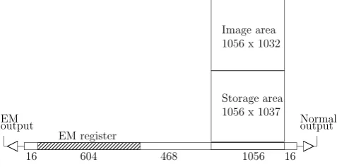
[image:2.595.307.544.57.241.2]Most EMCCDs are of frame-transfer design (see Fig. 1). Here, half the chip is covered with an opaque light shield that defines a storage area. The charge in this storage area can be transferred independently of that in the image area. This allows an image in the storage area to be read out concurrently with the integration of
[image:2.595.43.282.533.651.2]Figure 1. Schematic structure of an EMCCD, the E2V CCD201. Photo-electrons produced in the image area are vertically clocked downwards, first into the storage area, and then into the 1056-pixel serial register. For EM-CCD operation, the charge is then horizontally clocked leftwards, through the 468-pixel extended serial register and into the 604-pixel EM register, be-fore being measured and digitized at the EM output. For conventional CCD operation, the charge in the serial register is horizontally clocked rightwards to the normal output.
Figure 2. The geometry of the serial and EM registers, showing how multi-plication occurs. The top part of the diagram shows a cross-section through the EMCCD structure with the electrode phases lying at the surface. Below this are three snapshots showing the potential wells and the charge packets they contain at key moments (t1, t2, t3) in the clocking process. At t3the photoelectrons undergo avalanche multiplication as they fall into the poten-tial well below the HV clock phase. Note that this diagram does not show a complete pixel cycle.
the next image, with just a few tens of millisecond dead time be-tween exposures. Incorporating frame-transfer architecture into any CCD will greatly improve observing efficiency in high frame-rate applications where the readout time is comparable to the required temporal resolution (Dhillon et al. 2007). In the case of an EMCCD the use of frame-transfer architecture is essential, otherwise the S/N gains will be nullified by dead time.
2.2 Multiplication noise
A single photoelectron entering the EM register can give rise to a wide range of output signals. This statistical spread constitutes an additional noise source termed multiplication noise (Hollenhorst 1990). Basden, Haniff & Mackay (2003) derive the following equa-tion describing the probabilityp(x) of an output xfrom the EM register in response to an input ofn(an integer) photoelectrons:
p(x)= x
n−1exp(−x/gA) gn
A(n−1)!
. (1)
Figure 3. Output of an EM register withgA=100 in response to a range of inputs from 1 to 5 e−. They-axis shows the probability density function (PDF) of the output signal, i.e. the fraction of pixels lying within a histogram bin.
2.3 Gain
Astronomers typically refer to the gain (or strictly speaking sys-tem gain,gS) of a CCD camera as the number of photoelectrons represented by 1 analogue-to-digital unit (ADU) in the raw image, i.e. it has units of e−/ADU. An EMCCD camera has another gain parameter that we need to describe: the avalanche multiplication gaingA(hereafter referred to as theEM gain), and there is a risk of confusion here withgS. EM gain is simply a unitless multiplication factor equal to the mean number of electrons that exit the EM reg-ister in response to a single electron input. It is hence related togS by the relationgA=gS0/gS, wheregS0is the system gain (in units of e−/ADU) measured with the EM gain set to unity.
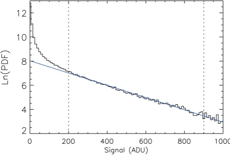
To measure the various EMCCD gain parameters, we need to first turn off the EM gain by reducing the HV clock amplitude to 20 V. At this level the EM register will then behave as a conventional se-rial register, i.e. 1 electron in, 1 electron out. We can now measure gS0, just as we would with a conventional CCD (there are various methods, for example the photon transfer curve; Janesick 2001). To measuregS, we weakly (<0.1 e− pixel−1) illuminate an EMCCD with a flat-field so as to avoid a significant number of pixels con-taining more than a single electron. A histogram of such an image, with a vertical log scale, is shown in Fig. 4. In this histogram, the pixels containing photoelectrons lie along a curve that is linear ex-cept at low values where the effects of read noise become dominant. Fig. 4 also shows a least-squares straight-line fit to the linear part of the histogram: the gradient of the line is equal to−gS(Tulloch 2004). In this particular case the camera had a system gaingS = 0.005 e−/ADU, i.e. a single photoelectron entering the EM register would produce a mean signal of 200 ADU in the output image. When discussing noise levels in an EMCCD it is more convenient to express this in units of input-referenced photoelectrons (e−pe). So in the above example, if the read noise is 5 ADU this would be quoted as 5×0.005=0.025 e−pe.
2.4 Clock-induced charge
Clock-induced charge (CIC) is an important source of noise in EMCCDs. Its contribution needs to be minimized. It consists of internally generated electrons produced by clock transitions during the readout process. CIC is visible in EMCCD bias frames as a scattering of single electron events which at first sight are
indistin-Figure 4. The histogram, plotted on a logevertical scale, of pixels in a weakly illuminated EMCCD image. The solid line is a least-squares linear fit to the photoelectron events lying between the two vertical dotted lines. The slope of this fitted line can be used to calculate the system gaingSof the camera in e−/ADU.
guishable from photoelectrons. It is only when a histogram is made of the image that they appear different.
CIC is dependent on a number of factors. The amplitude of the clock swings is relevant, as is the temperature (Janesick 2001). At first sight, one might assume that, since CIC is proportional to the total number of clock transitions a pixel experiences during the readout process, a pixel lying far from the readout amplifier should experience a higher level of CIC. One would then expect CIC gradients in both the horizontal and vertical axes of the image. This would be true if the CCD is entirely cleared of charge prior to each readout. However, this is never the case. One must consider that prior to each readout the chip has either been flushed in a clear operation or read out in a previous exposure. These operations leave a ‘history’ of CIC events in the CCD pixels prior to our subsequent measurement readout. The distribution of these historical events will be higher the closer we get to the output amplifier since the CIC charge residing in these pixels will have accumulated through a larger number of clock transitions than for pixels more distant from the amplifier. When these historical events are added to the events created in the most recent measurement readout the overall effect is that each pixel of the image will have experienced the same number of clock transitions regardless of its position, and the resulting CIC distribution will be flat.
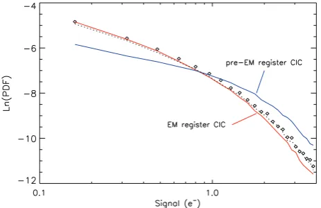
[image:3.595.310.546.57.216.2]Figure 5. Histogram (diamonds) of a QUCAM2 bias image compared with two models: pure in-register CIC and pure pre-EM register CIC. A fit to the data, consisting of 85 per cent CIC generated within the EM register and 15 per cent generated prior to the EM register, is shown as a dotted curve. of CIC originating at random positions within the EM register. The latter will on average experience less multiplication than the former since it will pass through fewer stages of the multiplication register, producing a histogram that shows an excess of low value pixels (as shown in Fig. 5). Various other models were created with mixes of the two noise sources. The best fit was found to correspond to 85 per cent CICIR and 15 per cent pre-EM-register CIC, demonstrating that QUCAM2 has been well optimized (at least as far as its CIC performance is concerned with some other parameters such as CTE remaining non-optimal) and is dominated by CICIR. Details on the final performance of QUCAM2 and the values of some of its more critical parameters can be found in Table 1. Pre-EM register CIC electrons should not be confused with dark current generated during the readout. These can easily outnumber CIC events if the operational temperature is too high, if the CCD controller has recently been powered on or if the CCD has recently been saturated to beyond full-well capacity. The recovery time for these last two cases is approximately 2 h, and an accurate measurement of CIC should not be attempted until after such a period.
Table 1. QUCAM2 technical details.
CCD type E2V CCD201-20
Controller ARC Gen. III
Operating temperature 178 K Pixel time (EM amplifier) 1.3µs Pixel time (normal amplifier) 5.1µs Frame-transfer time 13 ms
Row transfer time 12µs
EM multiplication gaingA 1840
HV clock rise-time 70 ns
HV clock fall-time 150 ns
HV clock voltage high 40 V (square wave) Parallel clock voltages −1/+8 V Serial clock voltages 0/+8.5 V Substrate voltage +4.5 V Read noise (EM amplifier) 40 e− Read noise (normal amplifier) 3.1 e− Mean charge in bias image 0.013 e−pixel−1 Cosmic ray rate 0.9 e−pixel−1h−1 Image area dark current 1.5 e−pixel−1h−1 EM register CIC probability 1.4×10e−4transfer−1 EM register (1e−level) CTE 0.999 85
CIC electrons generated within the EM register do not contribute as much charge to an image as a CIC electron generated prior to the register: CICIR has a fractional charge when expressed in units of input-referenced photoelectrons. If we assume that CICIR is generated randomly throughout the EM register then we can calculate the average chargeνCthat it will contribute to an image pixel. The calculation, derived in Appendix A, shows that
νC≈ BC
ln(gA), (2)
whereBC is the mean number of CICIR events experienced by a pixel during its transit through the EM register.
2.5 Non-inverted mode operation
If the vertical clock phases are held more than about 7 V below sub-strate then the surface potential of the silicon underlying the phases becomes pinned at the substrate voltage (so-called Inverted-mode operation or IMO). This has important consequences for both dark current and CIC. If during the read-out of the image the clock phases never become inverted (so-called non-inverted mode operation or NIMO) then the CIC is greatly reduced (in the case of QUCAM2 it fell from 0.2 e−pixel−1to a level that was unmeasurable even after 50 bias frames had been summed). At higher operational temper-atures NIMO will cause an approximate 100-fold increase in dark current: something that will negate any gains from lowered CIC. The trade-off between CIC and dark current does not, however, hold at lower temperatures. For QUCAM2 at an operational tem-perature of 178 K, the NIMO dark current was 1.5 e−pixel−1h−1, a value that was found to be constant for exposure times of up to 1000 s. Switching to IMO reduced this to∼0.2 e−pixel−1h−1: a value somewhat difficult to measure since it is nearly four times be-low the current delivered by cosmic ray events. This demonstrates that operation at cryogenic temperatures permits NIMO without a loss of performance from high dark current. It should be noted that at higher temperatures, such as those experienced by Peltier-cooled CCDs, the situation becomes more complex since dark current is no longer constant with exposure time. This effect was seen dur-ing the optimization of QUCAM2 when operated experimentally at 193 K. Using NIMO, the dark current for 60 s exposures was measured at 12 e−pixel−1h−1 whereas for 600 s exposures it was 40 e−pixel−1h−1.
3 M O D E S O F E M C C D O P E R AT I O N
EMCCDs can be utilized in three separate modes, each offering optimum S/N in certain observational regimes. In this section the equations describing the S/N in these three modes are shown.
3.1 Conventional mode
The S/N obtained through the conventional low-noise amplifier is given by
SNRC=
M
M+νC+D+K+σ2 N
, (3)
3.2 Linear mode
In linear mode, the digitized signal from the EM output is interpreted as having a linear relationship with the photoelectrons, as is usual for a CCD. The S/N obtained through the EM output is then given by
SNRlin=
M
2.(M+νC+D+K)+(σEM/gA)2. (4)
The factor of 2 in the denominator accounts for the multiplication noise (see Section 2.2). The derivation of this factor can be found in Marsh (2008) and Tubbs (2003). The read noise in the EM amplifier σEMwill typically be tens of electrons due to its higher bandwidth but its contribution to the denominator is rendered negligible by the use of high EM gain,gA. High speed means high read noise so high frame-rate cameras will need higher gains than the more leisurely QUCAM2 (1.6 s read-out time in EM mode).
3.3 Photon-counting mode
In PC mode we apply a threshold to the image and interpret any pixels above it as containing a single photoelectron. This leads to coincidence losses at higher signal levels where there is a significant probability of a pixel receiving two or more photoelectrons, but at weak signal levels where this probability is low, PC operation offers a means of eliminating multiplication noise (Plakhotnik, Chennu & Zvyagin 2006) and obtaining an S/N very close to that of an ideal detector. When PC we must aim to maximize the fraction of genuine photoelectrons that are detected whilst at the same time minimizing the number of detected CICIR and read noise pixels. Fig. 6 shows how this can be done. The graph shows us that if we set a PC threshold of, say, 0.1 e−pe(a value that was later found to be optimum; see Section 4.5) we will detect 90 per cent of photoelectrons but only 23 per cent of the CICIR. False counts from the read noise will be negligible. The S/N of an ideal PC detector, including the effects of coincidence losses, is given by
SNRpc= M
√
eM−1. (5)
[image:5.595.311.543.53.292.2]This equation (derived in Appendix B) needs to be modified to accurately describe a PC EMCCD since it makes no allowance for the complex effects of CICIR and choice of threshold level. Since the distribution of CICIR and photoelectron events are dif-ferent, the S/N can vary greatly depending on the precise choice
[image:5.595.52.279.544.695.2]Figure 6. The effect of the PC threshold value on the detected fraction of the signal, the CIC and the read noise in an EMCCD image. In this case the read noiseσEM=0.025e−peandgA=2000.
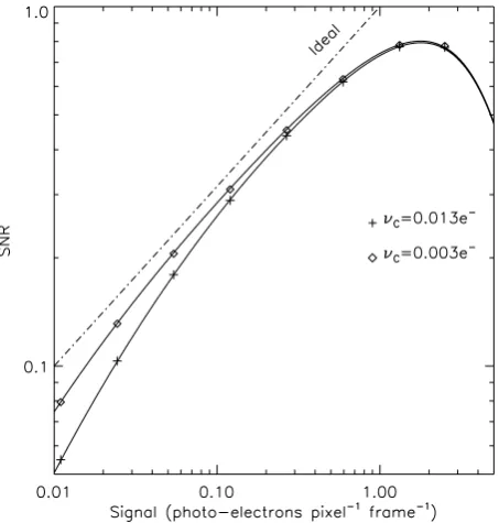
Figure 7. The relative S/N (compared to an ideal noise-free detector of the same QE) of each EMCCD mode (conventional, linear and PC) is shown over a wide range of illuminations. The solid curves show the performance of a detector identical to QUCAM2 (νC=0.013 e−,σN=3.1 e−), and the dotted lines show the performance that would be expected from a more highly optimized detector (νC=0.003 e−,σN=2.6 e−).
of threshold. These complexities have been explored in detail by modelling (see Section 4) but, in short, the following S/N relation (derived in Appendix C) is found to hold, assuming a PC threshold of 0.1 e−pe(close to optimum, see Section 4.5):
0.9M
√
δ√exp [(0.9(M+D+K)/δ)+0.23 ln(gA)νC]−1
. (6)
It should be noted that the maximum possible S/N in a single PC frame is≈0.8 (see Fig. 11) and it is then necessary to average many frames to arrive at a usable image (i.e. one with S/N> 3). The number of frames that would need to be ‘blocked’ together in this fashion is given the symbolδin equation (6).
3.4 Optimum choice of mode
Considered from the point of view of maximizing the S/N per pixel, the choice of readout mode is quite simple. Fig. 7 shows the range of per-pixel illuminations over which each mode offers the best S/N, based on the equations presented earlier in this section. A single pixel is, however, not usually the same thing as a single wavelength element in a reduced spectrum. Many additional factors affect the choice of mode, such as plate scale, seeing and sky background, and this is explored in greater depth in Section 5.
4 M O D E L L I N G P H OT O N - C O U N T I N G P E R F O R M A N C E
4.1 What was modelled
Equation (1) describes the output of an EM register for any integer number nof photoelectrons. Using the Poisson distribution it is possible to calculate the proportion of pixels that containn=1, 2, 3. . .photoelectrons as a function of the mean illuminationM. This result can be combined with equation (1) to yield the output distribution of the EM register for any mean input signal level. No equivalent relation describing the output distribution of CICIR could be found, and it is here that Monte Carlo modelling is required (see Section 4.2).
The final output of the model is a pair of 3D vectors. The first of these shows the output pixel value distributions (i.e. histograms) for a wide range of signal and CICIR levels. The second is the associated cumulative distribution function (CDF) derived from the histograms in the first 3D vector. The CDF is extremely useful since it indicates the mean photon counts per pixel that we can expect for any combination of signal and CICIR for any given PC threshold. These 3D vectors can be visualized as two cubes of normalized histogram values and CDF values. The x-axis of the cubes is labelled with a logarithmic-spaced range of CIC values and the y-axes with a logarithmic-spaced range of signal values (extending up to a maximum of 2.5 e−). Thez-axes are labelled with pixel values extending up to a maximum of 10 e−pe. In the case of the CDF cube, thez-axis units can also be interpreted as the PC threshold setting and the data values as being the mean per pixel-PC signal at that given threshold. To illustrate what we mean, we show some sample data taken from the first of these 3D vectors in Fig. E1.
4.2 Modelling of CICIR
Since no analytical formula describing the distribution of CICIR events could be found it was necessary to do a Monte Carlo model of the EM register. Binomial statistics describe processes whose final outcome depends on a series of decisions each of which has two possible outcomes. It therefore applies to the creation of CIC as a pixel is clocked along the EM register. Synthetic images were generated containing between one and six CIC events per pixel. It was not really necessary to go any higher than six CIC events since the binomial distribution shows that there is an insignificant probability of more than six events being generated per pixel for mean CIC event levels of up to 0.3 per pixel, well beyond the useful operational range of an EMCCD (indeed QUCAM2 gave∼0.08 CIC events per pixel). Histograms of these six images were then calculated to yield a set of output CIC distributions for integer in-put, analogous to the distributions for photoelectron events given by equation (1). It was then necessary to combine these histograms us-ing the binomial distribution formula to yield the output distribution of the EM register for anymeanCIC event level.
The model was implemented by simulating the transfer of charge through an EM register with 604 elements, one pixel at a time. At each pixel transfer a dice was thrown for each electron in the pixel to decide if a multiplication event occurred. An overall EM gain of gA=2000 was used. Six thousand lines were read out in this way to get a good statistical sample of pixel values. At the start of the read-out of each simulated image row, the EM register was charged with a single electron per element. This simply amounted to initializing the array representing the EM register with each element equal to 1. This was then read out, simulating the effect of charge amplification, to yield an image with width equal to the length of the register. The resulting image was then scrambled (i.e. the pixels were reordered
in a random fashion) and added to its original self to yield an image containing an average of two CIC events per pixel. This scrambling was necessary since the raw images contained pixels with values that were approximately proportional to their column coordinate, with the pixels in the higher column numbers having higher values. Further scramble-plus-addition operations were performed to yield images with three, four, five and six events per pixel.
4.3 Modelling of realistic EMCCD images
The distributions of the CICIR (calculated in Section 4.2) and the distribution of the photoelectron events were then combined, to-gether with read noise, through the use of intermediate model im-ages. Photoelectron events were first generated in the image using a random number generator that was weighted by the distribution of the EM register output. CICIR events were then added to the image in the same manner as for the photoelectrons. Finally, read noise ofσEM=0.025 e−pe was added to every pixel in the image. These model images contained a bias region from which photoelectrons were excluded. Histograms of the image and bias regions were then calculated to yield the distributions and their CDFs. These CDFs ef-fectively gave the mean PC signal from the image and bias areas as a function oftthe PC threshold. The S/N could then be determined using the following equation (derived in Appendix B):
SNRpc(t)=
−ln[1−CDFI(t)]+ln[1−CDFB(t)]
[1−CDFI(t)]−1−1
, (7)
where CDFI and CDFB are the image and bias area CDFs, re-spectively. Since the CDFs were calculated over a wide range of threshold values it was possible to find the optimum threshold value or alternatively just calculate the S/N for any given threshold.
4.4 Testing of the model
[image:6.595.309.541.553.707.2]The model output was tested against a stack of 45 QUCAM2 bias frames of known CIC level, EM gain and system gain. The compar-ison between model and data is shown in Fig. 8. The agreement is good, although QUCAM2 shows a slight excess of low value events compared to that predicted. This can be explained by the imperfect charge transfer in the EM register which boosts the relative number of low-value events, an effect that was not included in the model.
4.5 Optimum PC threshold
[image:7.595.333.522.55.218.2]It is the read noise that sets the lower limit on the PC threshold. Gaussian statistics predict that a threshold set∼3σabove this noise gives one false count per 1000 pixels, falling to one pixel in 32 000 if we choose a threshold of 4σ. Other groups (Daigle, Carignan & Blais-Ouellette 2006; Ives et al. 2008) have chosen quite high thresholds (5–5.5σ). This is a good choice as long as it is combined with a high EM gain, high enough to ensure that the mean level of a photoelectron is at least 10 times the threshold value. This high ratio between mean photoelectron level and read noise permits a threshold to be set low enough to include a majority of photoelec-trons. There is a limit to how high the EM gain should be pushed, though, since it can risk damage to the chip if gain is applied during overexposure for long periods.
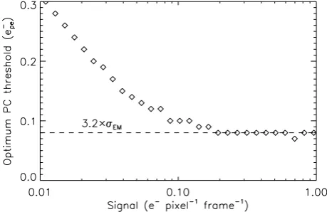
[image:7.595.50.280.537.686.2]Fig. 9 shows that the PC threshold needs to be tuned depending on the signal level, so that the maximum number of genuine photoelec-trons are counted and the maximum number of CICIR are rejected. Fig. 9 also shows that in the case of a detector with read noiseσEM= 0.025 e−pe, the optimum threshold falls as low as 3.2σEM. From a data-reduction point of view, using a variable threshold adds com-plexity but may be necessary to extract maximum S/N, particularly at low signal levels. One example of this would be the measurement of a faint emission line, the peak of which would be placed at an optimum signal level through a suitable choice of frame rate. Here, the threshold would be set low, in the region of 0.1 e−peaccording to Fig. 9. The wings of this same line, which may be an order of magnitude fainter would then benefit from an increased threshold, say∼0.25 e−pe. The use of an adaptive threshold would create many side effects, such as noise artefacts (the amount of background sig-nal from CIC, sky and dark current would be modified depending on threshold setting), so would require extra data reduction effort. Note also that non-Gaussian pattern noise is a particular problem in high-speed detectors in an observatory environment which may require the threshold to be pushed higher than would otherwise be optimum. The models described so far have assumed a read noise of 0.025 e−pe(equal to that of QUCAM2). A simulation was performed of the effect of higher (0.05 e−pe) and lower (0.012 e−pe) read noise on the S/N performance of an EMCCD. Whilst the higher noise definitely impinges on the PC performance by forcing the threshold higher and giving a lower detected fraction of photoelectrons, the lower noise gives very little additional benefits. This can be ex-plained by the fact that the bulk of the CICIR has a distribution that
Figure 9.The PC threshold that gives maximum S/N is plotted as a function of signal level. Model images were used with parameters close to those of QUCAM2. The read noiseσEMwas 0.025 e−peand the multiplication gain
gAwas 2000.
Figure 10. The autocorrelation of a weakly illuminated QUCAM2 image showing the elongation of the single electron events through CTE degrada-tion in the EM register.
falls between 0 and 0.05 e−peand it will dominate any read noise lying within the same range. In the specific case of QUCAM2 there is an additional reason (apart from staying above the read noise) why the threshold must be kept slightly elevated. This is the effect of poor charge transfer efficiency (CTE) in the EM register. Fig. 10 shows the autocorrelation of a low-level flat-field which demonstrates the problem. The autocorrelation was performed along an axis parallel to the serial register. The slight broadening of the autocorrelation peak is indicative of less-than-perfect CTE. Using a threshold much below 0.1 e−pewould cause complex effects from multiple counting of single electron events due to the slight tail on each event being above the threshold.
Note that Basden et al. (2003) have modelled a multiple threshold technique that can extend PC operation well into the coincidence-loss-dominated signal regime (see Section 3.3) whilst maintaining high performance.
4.6 Simplification of S/N equation in PC mode
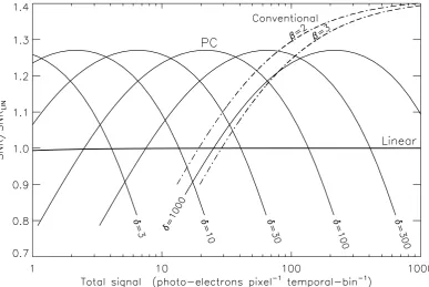
Figure 11. The S/N of two hypothetical EMCCDs in PC mode, one with CICIRνCequal to that of QUCAM2, another withνCequal to that which might be obtained in a more optimized detector.gAin both cases is 2000 and the read noise is 0.025 e−pe. The crosses and stars show the predictions of the Monte Carlo model (equation 7); the solid lines show the approximation (equation 6). The S/N of an ideal detector (one where the S/N=√Signal) is plotted as a dot–dashed line for comparison.
4.7 S/N predictions from model
The model was used to evaluate the PC S/N (SNRpc) over a range of CIC and signal levels. The results are shown in Fig. 12, expressed both as a fraction of the S/N of an ideal detector S/Nideal and the
S/N of an EMCCD operated in linear mode SNRlin (as described in equation 4). The ideal detector is assumed to have the same QE as the EMCCD but does not suffer from read noise, coincidence or threshold losses. The figures reveal the presence of a PC ‘sweet-spot’, where an S/N in excess of 90 per cent of ideal is possible if the CIC can be sufficiently reduced (to aroundνC=0.002 e−pixel−1). The sweet-spot is quite narrow and extends between signals of
≈0.07 and 0.2 e−pixel−1. The plots also show that for signals of less than 1.2 e−pixel−1, PC is superior to linear-mode operation, and this is fairly independent of CIC level.
Fig. 12 shows that the sweet-spot of an EMCCD actually covers a very small range of exposure levels, however, we can effectively slide the sweet-spot along the per-temporal-bin exposure scale to quite high signal levels through the use of blocking, i.e. summing together a number of frames whose total exposure time equals our required temporal resolution. For QUCAM2, if we use the fairly generous definition of the sweet-spot as occupying the exposure range over which SNRpc>SNRlinthen this dynamic range is about 30:1. This would be like using a normal science CCD camera with a 7-bit (16-bit being more usual) analogue to digital converter (ADC) and could cause problems if the spectrum we wish to observe has a set of line intensities that exceeds this range.
5 R E C I P E F O R U S I N G A N E M C C D F O R A S T R O N O M I C A L S P E C T R O S C O P Y
The QUCAM2 camera at the WHT is used here as the basis of an example of how to correctly set up an EMCCD to maximize the S/N of a spectroscopic observation. The general principles outlined here, however, apply to any EMCCD camera.
[image:8.595.46.548.450.699.2]QUCAM2 is a relatively slow camera giving a minimum frame time in EM mode of 1.6 s. This then dictates the highest temporal resolution that is available. The small size of the CCD means that when used on the ISIS spectrograph it measures only 3.3 arcmin
Figure 13.The fluxmthat can be expected from each grating on ISIS when used with QUCAM2 as a function of source magnitude.R-band magnitudes as shown for theRgratings andB-band magnitudes for theBgratings. Calculated for airmass=1.
in the spatial direction. Full frame readout is then generally needed in order to locate a suitable comparison star for slit-loss correction, and this frame rate will therefore be hard to improve upon through the use of windowing. The linear EM mode should be considered as the default mode about which the observations are planned. The reason for this is that it gives an S/N that is a constant fraction of an ideal detector for almost all signal levels (see Fig. 7). The observer will not go far wrong by selecting this mode. It may be possible to coax extra S/N (as much as 40 per cent) from the observations by switching to one of the other modes but if the observation is not prepared carefully the data could prove useless. With linear mode the observer is guaranteed a practically noise-free detector without the dangers of potential coincidence losses and worse S/N than with a conventional CCD.
The first stage in planning the EMCCD observation is to refer to Fig. 13. This allows us to calculatem, the flux per pixel step in wavelength that we can expect from the object at our chosen spectral resolution. Using this datum we then need to refer to Fig. 14 to see how many seconds of observation (TSNR1) would be required on our object, using an EM detector in linear mode, to reach an S/N=1 in the final extracted spectrum. Fig. 14 shows the calculated times for both dark and bright-sky conditions (new and full moon) for both arms of ISIS. Seeing of 0.7 arcsec and a slitwidth of 1 arcsec have been assumed. Given that the spatial plate-scale of QUCAM2 on ISIS is 0.2 arcsec pixel−1, this implies that each wavelength element in the final extracted spectrum contains approximately five pixels worth of sky (assuming the spectrum is extracted across∼1.5×full width at half-maximum (FWHM) pixels in the spatial direction). Once we know the time it takes to reach an S/N= 1, it is then straightforward to calculate the time needed to reach any arbitrary S/N, since with linear mode, the S/N is proportional to the square root of the observation time.
The observer can now either play safe and use linear mode or explore the possibility of up to 40 per cent higher performance from either PC or conventional modes. This will depend on the mean per-pixel signal (from all sources including the sky) that we
can expect during an exposure of duration equal to our required temporal resolution,τ. This is calculated as follows:
signal pixel−1=τsky+m d
, (8)
wheredis the seeing-induced FWHM of the spectrum along the spatial axis of the CCD frame, measured in pixels. This dictates what spatial-binning factor we later need to use when extracting the spectrum. Note that in conventional and linear mode,τ is defined by the individual frame time, whereas in PC mode we divideτ intoδseparate frames that are later photon counted and summed (in order to observe brighter objects without incurring coincidence losses). Now that we have an estimation of the per-pixel signal we can use Fig. 15 to find which mode will give the optimum S/N on a per-pixel basis. If we find we can use PC then, according to Fig. 15, the S/N gain will be∼25 per cent, which we can translate into less telescope time. The S/N increases as the square root of the observation time in PC and linear mode, since the detector is dominated by noise sources with variances that increase linearly with signal. If instead we find that we have enough photoelectrons to permit conventional mode, the reduction in the observation time is harder to estimate since the relatively high read noise gives a non-linear relation between the square root of the exposure time and the S/N. The saving in telescope time from use of conventional mode could, however, be as much as 50 per cent (relative to linear mode) as the per-pixel signal tends to higher and higher values and the read noise becomes insignificant relative to the Poissonian noise in the sky and target.
5.1 Worked example of the recipe
Figure 14. TSNR1, the observation time on the WHT required to reach an S/N of 1 in the final extracted spectrum with the ISIS blue (left-hand panel) and red (right-hand panel) gratings as a function of source brightness. The detector is QUCAM2 operated in linear mode. A slitwidth of 1 arcsec, seeing of 0.7 arcsec and a spectral extraction over 5 pixels in the spatial direction are assumed. Observations are in theBband (left) andRband (right).
[image:10.595.101.489.418.677.2]To begin this problem, we use Fig. 13 to establish the signal that we can expect from the emission line. If we choose the R1200R grating (resolution∼7000) we will receive 0.07×4=0.28 photo-electrons per wavelength step per second. If we observe the object with a temporal resolution of 30 s we will be able to easily re-solve the eclipse. Referring to Fig. 14 we can then see that this combination of signal and spectral resolution will require∼7 s of observation to give an S/N=1 in the final extracted spectrum if we use linear mode. Since we can actually observe for 30 s, the S/N will be equal to√30/7=2.1.
We now turn to the choice of observing mode. Assuming 0.7 arcsec seeing, a slitwidth of 1 arcsec and that the spectrum will be extracted over 5 pixels in the spatial direction, we can cal-culate that the peak signal per temporal bin per pixel will be 0.28× 30/5=1.7 e−. To this, we must add the sky signal tabulated in Table E1. Since we are observing in dark time and at high resolu-tion this will be a negligible 0.003 e−s−1. Referring to Fig. 15 we can then immediately rule out conventional mode as the S/N would collapse at such a low signal level. The best mode would then be PC withδsomewhere between 3 and 10. Interpolating the figure we can estimate thatδ≈7 would be optimum. This is feasible since the minimum read-time for seven PC frames is 11.2 s with QUCAM2, well below the required temporal resolution of 30 s. In conclusion, we would obtain the best S/N by observing at a frame time of 4.3 s, PC the raw images and then averaging them into groups of seven to obtain our required time resolution. Tuning the exposure time in this way to keep the spectral line on the PC sweet-spot affords us a∼25 per cent S/N improvement over linear-mode operation (see Fig. 15).
Note that there is an upper limit to the useful PC blocking fac-torδ, set by the read noise of the conventional amplifier. Large blocking factors imply low-temporal resolution and there comes a point where it becomes favourable to use the conventional mode (see Fig. 15). The degree of off-chip binningβused is critical since this adds noise to conventional mode but not to PC mode.
In the case of QUCAM2, it can be demonstrated (using the S/N equations in Section 3) that the maximum useful blocking factor is
∼20σ2
Nβ. For larger values ofδthe S/N that can be obtained with conventional mode then exceeds the maximum obtainable with PC operation.
5.2 Binning
CCDs can be binned on-chip in a noiseless fashion in both axes. Since a spectrum will always be spread by seeing in the spatial direction, some degree of binning is often required. Some of this can be done on-chip but it is usual to do some of it off-chip (i.e. post-readout) during extraction of the spectrum.
An EMCCD will suffer much less from off-chip binning than a conventional detector, which has an effective read noise multiplied by the square root of the binning factor. As the off-chip binning factor β increases, the balance tips ever more in favour of the EMCCD.
5.3 Phase folding
For observations of objects that vary on a regular period, such as short-period binary stars, we can also consider extending our observations over many orbits and then ‘phase folding’ the data. This is an equivalent form of off-chip binning. It increases our signal by the folding factorγ and permits us to observe fainter sources or, alternatively, to observe the same source at higher time
resolution. If the S/N we require per wavelength element in our final extracted spectrum is given by SNRreq then the number of phase foldsγ we need to use (i.e. the number of orbits we must observe) in linear mode is given by
≈ TSNR1×SNR
2 req
τ . (9)
6 E M C C D S O N L A R G E T E L E S C O P E S
The performance of an EMCCD on an extremely large telescope and, in particular, the quantitative advantage it might give over a conventional CCD camera are explored in this section. Signal fluxes are calculated assuming a hypothetical ISIS-type instrument on the E-ELT (42-m aperture) using higher efficiency volume-phase holographic (VPH) gratings. These typically offer a 30 per cent in-crease in throughput over conventional diffraction gratings. Sky backgrounds from Paranal (approximately 20 km distant from the future E-ELT site) are assumed (Patat 2003). The QE of current EMCCDs are already very high (peaking at>90 per cent) and any future EMCCD is unlikely to be significantly different. The tempo-ral resolution as a function of source magnitude is calculated assum-ing that an S/N of 1 is required in each element of the final reduced spectrum. Equations (3) and (4) were used for these calculations. The results are shown in Fig. 16, where linear and conventional modes are compared with an ideal detector. Two seeing conditions are assumed: natural median seeing (0.6 arcsec) and that which may be obtained in theRband with adaptive optics (AO) correction (0.1 arcsec). With natural seeing and when observing very faint sources, long integrations are required. Under these conditions, the sky contribution becomes so high that the use of EMCCDs actu-ally degrades the S/N through the effects of multiplication noise. If instead AO is used, the sky contribution is considerably reduced and the EMCCD operated in linear mode gives an advantage right across the range of source intensities explored in the plot.
6.1 Need for high frame rates
Higher frame rates allow us to observe at higher time resolution, of course, but in the case of PC operation it also means we can avoid coincidence losses when observing brighter sources and cope with the higher sky backgrounds we can expect from the E-ELT’s larger collecting area. We always need to ensure that the per-pixel signal remains in the sweet spot (<0.2 e−; see Fig. 7), so even in dark time and at high spectral dispersion we would need (referring to Table E2) to operate at>0.5 Hz in the blue and>2 Hz in theRband if we wish to photon count on the E-ELT (natural median seeing is assumed).
6.2 Need for frame-transfer design
Figure 16. The temporal resolution versus source magnitude for two seeing conditions on an ISIS-type E-ELT instrument. The curves indicate the observation time required to reach an S/N of 1 in each wavelength element of the final extracted spectrum using a normal (non-FT) CCD, an FT CCD, an EMCCD in linear mode and an ideal detector. Off-chip spatial binning of×2 andσN=2.6 e−are assumed. The grating is a VPH equivalent of the ISIS R1200R grating, and we observe in theR-band during dark time. The slitwidth is assumed to be 1.5 times the seeing FWHM. The curve corresponding to the non-FT CCD assumes a 2 k×4 k detector (similar to that currently used on ISIS) with full-frame read out. An ideal detector is one with the same QE as a normal CCD but which has zero read noise.
is here that an FT CCD can give massive gains. The performance of a conventional CCD with non-FT architecture and 30 s dead time between exposures is shown plotted in Fig. 16. Any future CCD used on the E-ELT, especially if destined for high time-resolution applications, be it an EMCCD or otherwise, should incorporate FT architecture.
6.3 An EMCCD for the E-ELT
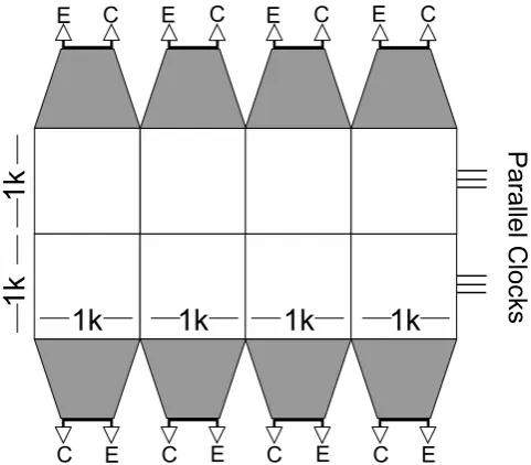
Current EMCCDs are rather small (1k×1k pixels). For spectroscopy this is not a good format since it limits our spectral range and also the availability of comparison stars near the target. Any EMCCD designed for use with the E-ELT therefore needs to be physically larger. It will require multiple outputs to achieve higher frame rates, so as to permit high time-resolution and allow PC mode operation. A possible geometry for such an EMCCD is shown in Fig. 17. Here a monolithic 4 k×2 k image area is proposed. Tapered stor-age areas are positioned both above and below the imstor-age area. Their shape provides space for multiple EM registers. This is sim-ilar to the architecture of the CCD220, a smaller format, multiple output EMCCD developed for wavefront sensing (Feautrier et al. 2008). In principle, the storage areas can be shrunk by reducing the height (in the axis perpendicular to the serial register) of their pixels. This results in more efficient use of the available silicon. It would be at the expense of reduced full-well capacity, but this is of little concern in the low-signal regime where EMCCDs are best applied. Each storage area can be read out through either a con-ventional amplifier capable of giving 2.6 e−noise at 200 k pixel s−1 or a higher-noise (20–30 e−) EM amplifier capable of running at 10 M pixel s−1. These amplifiers could be combined so that conven-tional mode would be selected simply by setting the EM gain to unity, but having two separate amplifiers allows more design
flex-Figure 17. A possible design for a future EMCCD for spectrographic use on the E-ELT. Conventional amplifiers are labelled C; EM amplifiers are labelled E. The shaded regions are the storage areas. Each 1 k×1 k pixel block has its own conventional and EM amplifiers, permitting faster parallel readout. This monolithic design is buttable along two edges allowing it to be extended horizontally for increased spectral coverage.
[image:12.595.306.547.384.595.2]register are kept at negligibly low levels. Full-frame readout would be possible in 5 s through the conventional amplifiers and in 0.1 s through the EM amplifiers. None of these design parameters, taken individually, exceeds those of current scientific cameras. We already know from discussions with E2V that such a device is feasible to manufacture, although the large pin-count may require the EM and conventional amplifiers to be combined. The spectral axis would lie horizontally in Fig. 17. This would maximize the spectral coverage and also allow efficient on-chip spatial binning in order to reduce the effects of CICIR and read noise, and to reduce the read time in close proportion to the spatial binning factor. Such a CCD would have a wide application in the field of high time-resolution spec-troscopy. In Fig. 16, it has already been shown that simply switch-ing to an FT design without implementswitch-ing an EM register can give a huge advantage. Considering the economics of the E-ELT, the extra expense required to implement FT architecture (which approximately doubles the area of silicon required) can be easily justified. The incremental expense of then adding an EM register (estimated at 10–20 per cent by E2V) will give excellent value for money given the further savings in telescope time that it can provide.
7 C O N C L U S I O N S
We have shown that EMCCDs are almost perfect detectors for optical spectroscopy. They have close to 100 per cent QE, virtu-ally no read noise, large formats, linear response, negligible dead time and are relatively inexpensive. Due to multiplication noise and CIC, however, they are not as straightforward to use as con-ventional CCDs, and care must be taken to ensure that they are operated in the correct mode: conventional, linear or PC. If EMC-CDs are used correctly, it is possible to gain orders-of-magnitude improvement in S/N compared to conventional CCDs at low light levels (see Fig. 7), but using the wrong mode can result in an orders-of-magnitude reduction in S/N. With the aid of Monte Carlo modelling of an EMCCD, we provide derivations of the S/N equa-tions for each EMCCD mode, and present a recipe for astronomers to assist in determining the optimum EMCCD mode for a given observation.
The EMCCD used in QUCAM2 and ULTRASPEC is the E2V CCD201-20 detector, which at 1 k×1 k pixels (each of 13×13µm) is the largest commercially available EMCCD. However, this is still substantially smaller than the conventional 4 k×2 k CCDs found on major optical spectrographs. As a consequence, using the CCD201 results in the loss of approximately three-quarters of the wavelength coverage and one half of the spatial coverage provided by typical astronomical spectrographs. This factor of 8 loss of detector area is a heavy price to pay, even for the huge S/N gains of an EMCCD. We therefore present a concept for a large-format EMCCD which can optimally sample the focal plane of the world’s major spec-trographs. It is important to emphasize that EMCCDs are identical to conventional CCDs in almost every respect (architecture, per-formance, read-out electronics), except for the fact that they have effectively zero read noise. This means that astronomers who do not have read noise limited observations lose nothing by using an EMCCD instead of a conventional CCD; in fact, we show that there will be significant efficiency gains (equivalent to approximately two weeks of time per year per telescope) because the frame-transfer format of EMCCDs results in essentially zero dead time compared to the tens-of-seconds dead time that conventional non-FT CCDs suffer from. The biggest gains, however, will be for astronomers
doing read noise limited spectroscopy, due to the fact that the read noise will also be zero. It is our firm belief, therefore, that once these large-format EMCCDs become available, they will become the detector of choice on the world’s major spectrographs including those to be built for the E-ELT.
AC K N OW L E D G M E N T S
We would like to thank Olivier Daigle for help with derivation of the PC equations.
R E F E R E N C E S
Basden A. G., Haniff C. A., Mackay C. D., 2003, MNRAS, 345, 985 Basden A. G., Haniff C. A., Mackay C. D., Bridgeland M. T., Wilson D.
M., Young J. S., Buscher D. F., 2004, in Traub W. A., ed., Proc. SPIE Vol. 5491, New Frontiers in Stellar Interferometry. SPIE, Bellingham, p. 677
Boksenberg A., Burgess D. E., 1972, in McGee J. D., McMullan D., Kahan E., eds, Photo-Electronic Image Devices. Acad. Press, London, p. 835 Daigle O., Carignan C., Blais-Ouellette S., 2006, in Dorn D. A., Holland
A. D., eds, Proc. SPIE Vol. 6276, High Energy, Optical, and Infrared Detectors for Astronomy II. SPIE, Bellingham, p. 42
Dhillon V. S. et al., 2007, MNRAS, 378, 825
Dhillon V. S., Marsh T. R., Copperwheat C., Bezawada N., Ives D., Vick A., O’Brien K., 2008, in Phelan D., Ryan O., Shearer A., eds, AIP Conf. Ser. Vol. 984, High Time Resolution Astrophysics. Am. Inst. Phys., New York, p. 132
Feautrier P., Gach J.-L., Balard P., Guillaume C., Downing M., Stadler E., Magnard Y., Denney S., 2008, in Dorn D. A., Holland A. D., eds, Proc. SPIE Vol. 7021, High Energy, Optical, and Infrared Detectors for Astronomy III. SPIE, Bellingham, p. 11
Hollenhorst J. N., 1990, IEEE Trans. Electron Devices, 37, 781 Hynecek J., 2001, IEEE Trans. Electron Devices, 48, 2238
Ives D., Bezawada N., Dhillon V. S., Marsh T. R., 2008, in Dorn D. A., Holland A. D., eds, Proc. SPIE Vol. 7021, High Energy, Optical, and Infrared Detectors for Astronomy III. SPIE, Bellingham, p. 10 Janesick J. R., 2001, Scientific Charge-Coupled Devices. SPIE Press,
Bellingham
Jenkins C. R., 1987, MNRAS, 226, 341
Jerram P. et al., 2001, in Blouke M. M., Canosa J., Sampat N., eds, Proc. SPIE Vol. 4306, Sensors and Camera Systems for Scientific, Industrial, and Digital Photography Applications II. SPIE, Bellingham, p. 178 Kanbach G., Stefanescu A., Duscha S., M¨uhlegger M., Schrey F., Steinle
H., Slowikowska A., Spruit H., 2008, in Phelan D., Ryan O., Shearer A., eds, Astrophys. Space Sci. Libr. Vol. 351, High Time Resolution Astrophysics. Springer, Berlin, p. 153
Mackay C. D., Tubbs R. N., Bell R., Burt D. J., Jerram P., Moody I., 2001, in Blouke M. M., Canosa J., Sampat N., eds, Proc. SPIE Vol. 4306, Sensors and Camera Systems. SPIE, Bellingham, p. 289
Marsh T. R., 2008, in Phelan D., Ryan O., Shearer A., eds, Astrophys. Space Sci. Libr. Vol. 351, High Time Resolution Astrophysics. Springer, Berlin, p. 75
Patat F., 2003, A&A, 400, 1183
Plakhotnik T., Chennu A., Zvyagin A. V., 2006, IEEE Trans. Electron Devices, 53, 618
Tubbs R. N., 2003, PhD thesis, Univ. Cambridge
Tubbs R. N., Baldwin J. E., Mackay C. D., Cox G. C., 2002, A&A, 387, L21
Tulloch S. M., 2004, in Moorwood A. F. M., Iye M., eds, Proc. SPIE Vol. 5492, Ground-based Instrumentation for Astronomy. SPIE, Bellingham, p. 604
Tulloch S. M., 2010, PhD thesis, Univ. Sheffield
A P P E N D I X A : F R AC T I O N A L C H A R G E O F C I C I R
A CIC electron originating within the EM register will effectively have a fractional charge whose value is equal to the average charge
¯
qOof a single photoelectron charge packet during its transit through the EM register. The instantaneous chargeqOof a pixel within the EM register that originated as a single photoelectron at the register input is
qO=(1+p)x, (A1)
wherexis the position within EM register andpthe per-transfer multiplication probability. The mean value, ¯qO, of this pixel during its EM register transit can then be obtained by integrating this function over the length of the register and then dividing by the number of stagesS. If we reference this charge to an equivalent signal at the input to the register, such thatqI=qO/gA, we get
¯ qI= 1
SgA S
x=1
(1+p)xdx. (A2)
This integral by the standard solution:
¯
qI= 1
SgAln(1+p)[(1+p) x
]Sx=1, (A3)
which gives the result
¯ qI=
1−gA−1
lngA ≈ 1
lngA. (A4)
Equation (A.4) now allows us to calculate the per transfer proba-bility of CICpCin the EM register from a knowledge of the gain gAand the mean CIC charge in the biasνC. The generation of this charge is a binomial process soBCthe total number of CIC events in a pixel exiting the EM register is given by
BC=pCS. (A5)
Since each of these CIC events will contain an average charge of ¯
qI, the mean per pixel CIC chargeνCis given by
νC=qIBC,¯ (A6)
substituting ¯qIfrom equation (A5) and rearranging, we get
pC≈
ln(gA)νC
S . (A7)
We can then show how the mean CIC charge in a pixelνC(relevant for linear-mode operation) and the mean number of CIC events in a pixelBC(relevant for PC operation) are related as follows:
BC
νC ≈ln(gA). (A8)
A P P E N D I X B : S / N O F A N I D E A L P H OT O N C O U N T E R
We present a full derivation of SNRpc, the S/N in a PC detector. This differs from that of an ideal detector due to the effects of coincidence losses. To the best of our knowledge this derivation has not appeared before in the astronomical literature.
LetNbe the mean illumination in photoelectrons per pixel andn the mean photon-counted signal per pixel, i.e. the fraction of pixels that contain one or more photoelectrons. Poisson statistics tell us that
n=1−e−N, (B1)
therefore
N= −ln(1−n). (B2)
The noise in a photon counted frame can be derived straightfor-wardly by considering that only two pixel values are possible: 0 and 1. Pixels containing 0 will have a variance ofN, those containing 1 will have a variance ofN −1. Knowing the fraction of pixels containing each of these two values then allows us to combine the variances in quadrature to yieldσpc, the rms noise:
σpc=[e−NN2+(1−e−N)(N−1)2], (B3)
=(e−N−e−2N). (B4)
The photon-counted images must then be processed to remove the effects of coincidence losses. This is done after the component frames within each temporal bin have been averaged to yield a mean value fornfor each pixel. The original mean signalNprior to coin-cidence losses is then recovered by using equation (B2). Although coincidence loss tends to produce a saturation and a smoothing of the image structure, the overall effect is to add a great deal of noise to the observation and for this reason we must avoid a PC detector entering the coincidence loss regime. The amount of extra noise generated can be calculated by considering the change dN inNproduced by a small change dNinn. The noise in the final coincidence-corrected pixel will then be equal to that in the unpro-cessed average pixel multiplied by dN/dn. From equation (B2) we get
N+dN = −ln[1−(n+dn)]. (B5)
This standard differential is then solved to yield
dN
dn =(1−n)
−1
. (B6)
SubstitutingNfornusing equation (B1) we get
dN dn =e
N. (B7)
We then multiply the uncorrected noise given in equation (B4) by this factor to yield the noise in the final coincidence-loss-corrected PC image. SNRpcis then given by
SNRpc= N
√
eN−1. (B8)
This can be expressed in units ofn, using equation (B2), which is more useful since it isnthat we actually measure from our images:
SNRpc=
−ln(1−n)
(1−n)−1−1. (B9)
A P P E N D I X C : S / N O F A P H OT O N - C O U N T I N G E M C C D
We have already shown in Appendix B that the S/N of an ideal photon counter is
SNRpc= N
√
eN−1, (C1)
withN representing the signal per pixel. This basic equation is now altered to a more realistic form to include the noise sources found in an EMCCD. Certain approximations are made during this process. The validity of these approximations have been verified by the Monte Carlo modelling.
to optimum and that at this level 90 per cent of photoelectrons and 23 per cent of CICIR will be detected. We then get
SNRpc=
0.9M
√
exp(0.9M+0.23BC)−1, (C2) whereMis the signal per temporal bin andBCthe number of CICIR events per pixel. We now need to consider that any PC observation will require the blocking ofδseparate images if we are to achieve a usable S/N (the S/N of a single PC image with the exposure level lying within the sweet-spot is≈0.4; see Fig. 11). We then get
SNRpc=
0.9M
√
[image:15.595.44.285.256.668.2]δ√exp(0.9M/δ+0.23BC)−1. (C3) Next, we need to include other noise sources such as skyKand dark chargeD(units of e−pixel−1). Since these are indistinguishable from photoelectrons they will have the same detected fraction for a given PC threshold. We also need to express the CICIR in terms ofνC(see equation A8), i.e. the mean per-pixel charge that CICIR
Figure D1.Some histograms generated by the EMCCD model, described in Section 4, are plotted here. These are taken from theIDLvariableOUT -PUTMIXHIST. In the upper panel are a set of histograms with the signal level varying from 0.001 to 2.5 e−pixel−1and with the CIC fixed atν
C= 0.001 e−pixel−1. The lower plot has the same range of signals but with
νC=0.03 e−pixel−1. The read noise was 0.025 e−pein both cases.
contributes to the image. This is a parameter that can be measured directly from the bias frames of an EMCCD camera. So we get
0.9M
√
δ√exp [(0.9(M+D+K)/δ)+0.23 ln(gA)νC]−1. (C4) Note thatνCthe CICIR is multiplied by a factor of ln(gA) in the de-nominator of equation (C4). This is a consequence of the fractional charge of a CICIR electron (see Appendix A).
Note also that the read noise has been entirely ignored in this simplified description. This is fair since the threshold was set well above the noise, resulting in very few false counts. The read noise has a secondary influence, however, since it causes an effective blurring of the threshold level. This ‘fuzzy-threshold’ must add some noise to the images since it can make all the difference as to whether an event lying close to the threshold is counted or not. The close fit between the approximation and the comprehensive model (see Fig. 11) would, however, indicate that this noise source is not significant.
A P P E N D I X D : M O D E L VA R I A B L E S
The data cube describing the count-rate from an EMCCD in PC mode as a function of the mean illumination, the mean number of CIC events per pixel and the threshold setting, is available as an IDL.sav file, together with descriptions of the variables it contains, at the following address: http://www.qucam.com/emccd/Histogram. html. It is included for those wishing to check our results or to perform their own experiments. Fig. D1 shows a selection of his-tograms extracted from the data cube by way of an example.
[image:15.595.363.496.453.538.2]A P P E N D I X E : S K Y B AC K G R O U N D S
Table E1.WHT+ISIS sky backgrounds with QUCAM2. Units: photoelectrons pixel−1s−1. Slitwidth=1 arcsec. From the ING web pages.
Grating Bright Dark
R316R 0.12 0.014
R600R 0.05 0.006
R1200R 0.023 0.003
R300B 0.07 0.004
R600B 0.03 0.002
R1200B 0.016 0.001
Table E2. Estimated sky backgrounds for an E-ELT+ISIS-type instrument with VPH gratings. The plate scale and the de-tector QE are assumed to be the same as for QUCAM2 on ISIS. Units: photoelec-trons pixel−1s−1. Slitwidth=1 arcsec.
Grating Bright Dark
Red 316 15 1.6
Red 600 6.0 0.7
Red 1200 2.7 0.4
Blue 300 8.2 0.47
Blue 600 3.6 0.23
Blue 1200 1.9 0.12
[image:15.595.363.495.613.697.2]