Iowa State University Patents
Iowa State University Research Foundation, Inc.
2-3-1987
Method of making a piezoelectric shear wave
resonator
Jin S. Wang
Iowa State University
Kenneth M. Lakin
Iowa State University
Allen R. Landin
Iowa State University
Follow this and additional works at:
http://lib.dr.iastate.edu/patents
Part of the
Electrical and Electronics Commons
This Patent is brought to you for free and open access by the Iowa State University Research Foundation, Inc. at Iowa State University Digital Repository. It has been accepted for inclusion in Iowa State University Patents by an authorized administrator of Iowa State University Digital Repository. For more information, please contactdigirep@iastate.edu.
Recommended Citation
Wang, Jin S.; Lakin, Kenneth M.; and Landin, Allen R., "Method of making a piezoelectric shear wave resonator" (1987).Iowa State University Patents. 134.
Method of making a piezoelectric shear wave resonator
Abstract
An acoustic shear wave resonator comprising a piezoelectric film having its C-axis substantially inclined from
the film normal such that the shear wave coupling coefficient significantly exceeds the longitudinal wave
coupling coefficient, whereby the film is capable of shear wave resonance, and means for exciting said film to
resonate. The film is prepared by deposition in a dc planar magnetron sputtering system to which a
supplemental electric field is applied. The resonator structure may also include a semiconductor material
having a positive temperature coefficient of resonance such that the resonator has a temperature coefficient of
resonance approaching 0 ppm/
Keywords
Electrical and Electronic Engineering
Disciplines
Electrical and Computer Engineering | Electrical and Electronics | Engineering
United States Patent [19]
Wang et al.
4,640,756
Feb. 3, 1987
[11]
Patent Number:
[45]
Date of Patent:
[54] METHOD OF MAKING A PIEZOELECI‘RIC SHEAR WAVE RESONATOR
[75] Inventors: Jin S. Wang, Harbor City, Calif;
Kenneth M. Lakin; Allen R. Landin,
both of Ames, Iowa
[73] Assignee: The United States of America as
represented by the United States
Department of Energy, Washington,
DC.
[21] Appl. No.: 736,164
[22] Filed:
May 20, 1985
Related US. Application Data
[63] Continuation-impart of Ser. No. 545,411, Oct. 25, 1983,
abandoned.
[51] Int. Cl.4 ... .. C23C 14/38
[52] US. Cl. ... ..204/192.18
L 204/192 C
[58] Field of Search ... .. 204/192 C, 192 SP, 192 PE,
204/192 R
[56] References Cited
U.S. PATENT DOCUMENTS
3,486,046 12/1969 Zalar . 3,558,351 l/l97l Foster . 3,573,960 4/1971 Duncan . 3,766,041 10/1973 Wasa et a1. . 3,846,649 11/1974 Lehmann et a1. . 4,142,124 2/1979 Ogawa et a]. . 4,164,676 8/ 1979 Nishiyama et al. . 4,229,506 10/1980 Nishiyama et a1. . 4,297,189 10/1981 Smith et a1. .
OTHER PUBLICATIONS
“UHF Composite Bulk Wave Resonators”, Lakin et al,
1980 IEEE Ultrasonics Symposium, p. 834.
“Acoustic Bulk Wave Composite Reactors”, Lakin et
al, Appl. Phys. Lett., 38 (3), p. 125, 2/1/81.
“Low-Temperature Coefficient Bulk Acoustic Wave
Composite Resonators”, Wang et al., Appl. Phys. Lett.,
40 (4), p. 308, 2/ 15/82.
“Aluminum Nitride Thin Film and Composite Bulk
COOLlNG WATER
TO DC POWER SOURCE
Wave Resonators”, Lakin et al., 36th Annual Fre
quency Control Symposium, 1982.
“Cadmium Sulphide and Zinc Oxide Thin-Film Trans
ducers”, Foster et al., IEEE Transactions on Sonics and
Ultrasonics, vol. SU-15, No. 1, p. 28.
“Variation of C—Axis Orientation of ZnO Thin Films
Deposited by DC Diode Sputtering”, Minikata et al., J. Appl. Phys., vol. 12, No. 3, p. 474.
“Highly Oriented ZnO Films by RF Sputtering of Hemispherical Electrode System”, Ohji et al., J. App. Phys., vol. 47, No. 4, Apr., 1976.
“Sputtered C-Axis Inclined Piezoelectric Films and Shear Wave Resonators”, Wang et al., 37th Annual
Symposium on Frequency Control, 1983.
“Thin Film Resonators and Filters”, Lakin et al., 1982
Ultrasonics Symposium.
“Sputtered C-Axis Inclined ZnO Films for Shear Wave
Resonators”, Wang et al., 1982 Ultrasonics Symposium.
“C-Axis Inclined ZnO Piezoelectric Shear Wave
Films”, Wang et al., App. Phys. Lett., 42 (4), 2/ 15/83.
Primary Examiner—John F. Niebling Assistant _Examiner—William T. Leader
Attorney, Agent, or Firm-James W. Weinberger;
Arthur A. Churm; Judson R. Hightower
[57]
ABSTRACT
An acoustic shear wave resonator comprising a piezo
electric ?lm having its C-axis substantially inclined
from the ?lm normal such that the shear wave coupling
coefficient signi?cantly exceeds the longitudinal wave
coupling coefficient, whereby the film is capable of
shear wave resonance, and means for exciting said film
to resonate. The ?lm is prepared by deposition in a dc
planar magnetron sputtering system to which a supple
mental electric ?eld is applied. The resonator structure
may also include a semiconductor material having a
positive temperature coefficient of resonance such that
the resonator has a temperature coefficient of resonance
approaching 0 ppm/°C.
U.S. Patent Feb. 3, 1987
Sheet 1 0m 4,640,756
0.4 1 I | I l | I I
ZnO
0.3 - -
0.2 _ -
COUPLING COEFFICIENT
O l I I l I l l l
0 IO 20 3O 4O 5O 6O 7O 8O 9O
C-AXIS ANGLE OF INCLINATION
F/G: M
0.3 | I I 1 | | l I
0.2 - -
COUPLING COEFFICIENT
O I I l I I I I |
0 IO 20 3O 4O 5O 6O 7O 8O 9O
C-AXIS ANGLE OF INCLINATION
US
Patent Feb. 3, 1987
Sheet2ofl3
4,640,756
/
COOLING WATER
TO DC POWER SOURCE
22.
US. Patent Feb. 3, 1987
Sheet5ofl3
4,640,756
O O 5
O O O O
O
O O O O
4 3 2 I
. . _ _
- _ _ - - P _ - - _ -
I /
. _ _ _ _
_
_
_ _
_
_ _ _ _
0 9
_ .
O
O
O
000
. O
o
7 5 3 l. I. 3 5
293.00 293. 20 293.40 293.60 293. 80 294.00
FREQUENCY (MHZ)
US. Patent Feb. 3, 1987
Sheet6ofl3
4,640,756
O
O
0
O0
0
O
O
5
O
50
5
3
2
2 ll
-
_
__
_
_ _ _ _ _ _ _ _ _ _
_ _ _ _ _ _
_ _
_ l
_ _ _
_ I
_
_ _
_
_ T
_ _
_ _
_ _|
_ _ _ _ _ _
_________________
OOOOOOOOOOO 9753||357_9
-
hwmmwme wozddmmsz 1O mw<Ia
420 410
385 390 395 400 405
FREQUENCY (MHZ)
380
‘U.S. Patgnt Feb. 3, 1987
Sheet7ofl3
4,640,756
m w
- _
,. _ _
_ _
-
O O O O 0
1w
750
730 740
FREQUENCY (MHZ)
720
US. Patent Feb. 3, 1987
Sheet80fl3
4,640,756
THICKNESS OF ZINC OXIDE
(Microns)
THICKNESS OF SILICON (Microns)
- _ _ _ _ _ -
O O O O O O O O O O O O O O O
[image:11.557.43.537.48.800.2]8 7 6 5 4 3 2 l
US. Patent Feb. 3, 1987
Sheet90fl3
4,640,756
IOOO | I l I I \ | | |
THICKNESS OF ALUMINUM NITRIDE _.
(Microns)
900
800
700
600
500
400
300
RESONANT FREQUENCY (MHZ)
200
I00 - —
O I 2 3 4 5 6 7 8 9 IO
THICKNESS OF SILICON (Microns)
US. Patent Feb. 3, 1987
Sheet 10 0f13 4,640,756
O
l 5
u N O
TEMPERATURE COEFFICIENT (PPM/°C)
_40 | | | | | 1 l | |
O | 2 3 4 5 6 7 8 9 IO
S'l/ZnO THICKNESS RATIO
Sheet 11 of 13 4,640,756
_ O O O O
I II 2
_ _
US. Patent Feb. 3, 1987
-30
Si/AIN THICKNESS RATIO
U.S. Patent Feb. 3, 1987
Sheet 13 of 13 4,640,756
soizmni .FZEQFEMOQ wmpzmwmiwk
-_O
O
0.1
O
O |
O
O I
mm
o
R.
Am
0
I
W0
20
T(
4WNO -
T|l||
AAAO
000 I
o,
__O_
0000
I254
4O 6O 80 I00 I20TEMPERATURE (°C)
20
4,640,756
1
METHOD OF MAKING A PIEZOELECI'RIC
SHEAR WAVE RESONATOR
CONTRACTUAL ORIGIN OF THE INVENTION
The U.S. Government has rights in this invention
pursuant to Contract No. W-7405-ENG-82 between the
U.S. Department of Energy and Ames Laboratory.
This application is a continuation-in-part of US. pa tent application Ser. No. 545,411, ?led Oct. 25, 1983,
now abandoned.
BACKGROUND OF THE INVENTION
This invention relates to a method of making ?lms of
piezoelectric materials suitable for preparing piezoelec
tric acoustic shear wave resonators and a method for
making said resonators.
Recent developments in electronics technology have
resulted in dramatic size reductions in electronic sys
terns, particularly those utilizing active semi-conductor devices. While many passive components have kept
pace with this size reduction, mechanical resonators
have not. The need for miniaturized resonators is par
ticulalry acute in the area of very large scale analog
integrated circuits associated with communications and
signal processing
Attempts at manufacturing suitable high-frequency
resonators have concentrated on the use of piezoelectric
resonator plates. However, piezoelectric plates for very
high and microwave frequencies are not amenable to
the conventional processing technology associated with
quartz or other traditional resonator materials. For
example, plates less than 10 pm thick are required in the
VHF to microwave frequency range, but mechanical
thinning of piezoelectric plates to the appropriate thick
ness is very dif?cult. In addition, for satisfactory reso
nance the plate surfaces must be parallel to a high preci
s1on.
It is known that resonators of suitable thinness and
parallelism may be attained with piezoelectric ?lms.
These ?lms may be manufactured by known means such as sputtering. Sputtered ?lms of common piezoelectric
materials show a strong tendency to grow with their C-axis perpendicular to the ?lm substrate. These ?lms are therefore suitable for longitudinal wave excitation
when driven by an electric ?eld perpendicular to the
?lm plane. v
For many applications it would be desirable to have a resonator suitable for excitation of shear waves rather
than longitudinal waves. Shear wave excitation is possi ble when the C-axes of 6 mm piezoelectric crystallites lie in the substrate plane and the crystallites are aligned
with one another. It is known that such ?lms may be deposited on a substrate of zinc, In2O3 or In2O3/SnO2, as described in US. Pat. No. 3,846,649 to Lehmann et
al. disclosing a piezoelectric transducer. However, at the present time there is no satisfactory technique for
growing C-axis inplane piezoelectric ?lms for general
application.
It has been calculated that, for piezoelectric materials
of 6 mm symmetry such as ZnO, AlN and CdS, a nearly
pure shear wave would be excited for ?lms having
C-axis orientation substantially inclined at an acute
angle with respect to the surface normal such that the shear wave coupling coef?cient signi?cantly exceeds the longitudinal wave coupling coef?cient, as reported by N. F. Foster, et al., IEEE Trans. on Sonics and
Ultrasonics, Vol. SU-l5, No. 1, Jan., 1968, p. 28. Under
10 25 30 35 40 45 50 55 65
2
these conditions, the quasi-shear-wave excitation will
greatly exceed the quasi-longitudinal-wave excitation,
and hence a good shear wave acoustic device can be
made. A C-axis angle of inclination of about 40° to about 50° is preferred. Foster et al. acknowledged that at the time of their writing such ?lms could not be
made. Ibid. at 40. Attempts have since been made to
sputter deposit C-axis inclined ZnO ?lm by placing the
substrate at a 90° angle with respect to the target, as
described by M. Minakata et al., Japan. J. Appl. Phys, Vol. 12, 1973, p. 474. However, the resulting ?lms have
uneven thickness and a mean C-axis variation unsuitable
for device applications. In addition, it would be desir able for the response of the resonator to be relatively
constant over a range of operating temperatures.
SUMMARY OF THE INVENTION
It is thus one object of the invention to provide a method of preparing thin ?lms of piezoelectric material suitable for preparing a piezoelectric acoustic shear
wave resonators.
It is yet another object of the invention to provide a
piezoelectric acoustic shear wave resonator which has a response which is relatively constant over a range of
operating temperatures. -
It is still another object of the invention to provide a method of making a piezoelectric acoustic shear wave
resonator.
Additional objects, advantages, and novel features of
the invention will be set forth in part in the following
description.
In accordance with the invention, a method is dis
closed for preparing a piezoelectric ?lm having its C
axis substantially inclined at an acute angle with respect
to the ?lm normal such that the shear wave coupling
co-ef?cient of said ?lm signi?cantly exceeds the longi
tudinal wave coupling coef?cient, whereby the ?lm is
capable of shear wave excitation. The ?lm may be made suf?ciently thin so that the excited shear waves are in
the microwave region. The ?lm is made of piezoelectric
materials having 6 mm symmetry such as ZnO and AlN.
The ?lm is provided with electrodes on opposite sides
to form an acoustic shear wave resonator.
The resonator of the instant invention is prepared by
growing a ?lm of a piezoelectric material on a substrate in a d.c. reactive sputtering system to which a supple
mentary electric ?eld is applied from a control elec
trode near the substrate. The electric ?eld has an orient
ing effect on the growing ?lm, such that the angle of
inclination of the C-axis of the ?lm with respect to the substrate is a function of the voltage of the applied ?eld, the distance of the electrode above the substrate and the lateral distance of the electrode from the substrate. After deposition the substrate may be etched away
under a central portion of the ?lm so that the ?lm is
supported by the substrate only at its periphery. Elec
trodes may be provided to both sides of the ?lm by
known means such as sputter deposition to form a shear
wave resonator.
In another embodiment a layer of doped semiconduc tor material having a positive temperature coef?cient of
resonance may be incorporated into the resonator struc ture to compensate the temperature coef?cient of reso
nance of the piezoelectric ?lm such that the tempera
ture coef?cient of resonance of the composite structure
4,640,756
3
resonance of the resonator is relatively constant over a
range of operating temperatures.
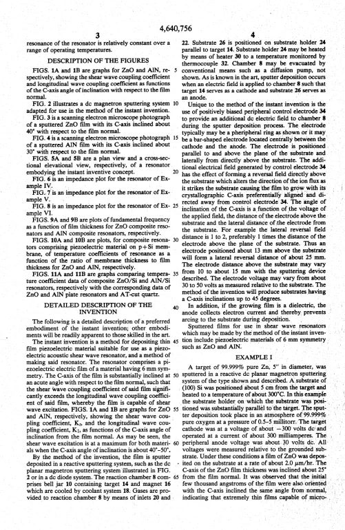
DESCRIPTION OF THE FIGURES
FIGS. 1A and 1B are graphs for ZnO and AlN, re
spectively, showing the shear wave coupling coef?cient
and longitudinal wave coupling coef?cient as functions of the C-axis angle of inclination with respect to the ?lm
normal.
FIG. 2 illustrates a dc magnetron sputtering system adapted for use in the method of the instant invention.
FIG. 3 is a scanning electron microscope photograph
of a sputtered ZnO ?lm with its C-axis inclined about
40’ with respect to the ?lm normal. ,
FIG.‘ 4 is a scanning electron microscope photograph
of a sputtered AlN ?lm with its C-axis inclined about 30’ with respect to the ?lm normal.
FIGS. 5A and 5B are a plan view and a cross-sec
tional elevational view, respectively, of a resonator
embodying the instant inventive concept.
FIG. 6 is an impedance plot for the resonator of Ex
ample IV.
‘ FIG“ 7 is animpedance plot for theresonatorof Ex-l
ample V. ,
FIG. 8 is an impedance plot for the resonator of Ex
ample VI.
FIGS. 9A and 9B are plots of fundamental frequency
as a function of ?lm thickness for ZnO composite reso
nators and AlN composite resonators, respectively.
FIGS. 10A and 10B are plots, for composite resona tors comprising piezoelectric material on p+Si mem
brane, of temperature coefficients of resonance as a
function of the ratio of membrane thickness to ?lm
thickness for ZnO and AlN, respectively.
FIGS. 11A and 11B are graphs comparing tempera ture coef?cient data of composite ZnO/Si and AlN/ Si
resonators, respectively with the corresponding data of
ZnO and MN plate resonators and AT-cut quartz.
DETAILED DESCRIPTION OF THE INVENTION
The following is a detailed description of apreferred embodiment of the instant invention; other embodi
ments will be readily apparent to those skilled in the art.
The instant inventionis a method for depositing thin
?lm piezoelectric material suitable for use as a piezo electric acoustic shear wave resonator, and a method of
making said resonator. The resonator comprises a pi
ezoelectric electric ?lm of a material having 6 mm sym
metry. The C-axis of the ?lm is substantially inclined at an acute angle with respect to the ?lm normal, such that
the shear wave coupling coef?cient of said ?lm signi? cantly exceeds the longitudinal wave coupling coef?ci ent of said ?lm, whereby the ?lm is capable of shear
wave excitation. FIGS. 1A and 1B are graphs for 2110
and AlN, respectively, showing the shear wave cou- ‘
pling'coef?cient, K3, and the longitudinal wave cou
pling coef?cient, K1, as functions of the C-axis angle of
inclination from the ?lm normal. As may be seen, the shear wave excitation is at a maximum for both materi
als when the C-axis angle of inclination is about 40°-50°.
By the method of the invention, the ?lm is sputter
deposited in a reactive sputtering system, such as the dc
planar magnetron sputtering system'illustrated in FIG.
2 or in a dc diode system. The reaction chamber 8 com
prises bell jar 10 containing target 14 and magnet 16
which are cooled by coolant system 18. Gases are pro
5 20 25 30 35 45 55 60
4
22. Substrate 26 is positioned on substrate ‘holder 24 parallel to target 14. Substrate holder 24 may be heated by means of heater 30 to a temperature monitored by
thermocouple 32. Chamber 8 may be evacuated by
conventional means such as a diffusion pump, not
shown. As is known in the art, sputter deposition occurs
when an electric field is applied to chamber 8 such‘that
target 14 serves as a cathode and substrate serves as
an anode. ‘ ‘
Unique to the method of the instant invention is the use of positively biased peripheral control electrode 34 to provide an additional dc electricl?eld t‘ochamber 8 during the sputter deposition process. The electrode ‘ typically may be a pheripheral ring as‘shown or it may‘
be a bar-shaped electrode located centrally between the‘
cathode and the anode. The electrode is positioned . parallel to and above the plane of the substrate and
laterally from directly above, the substrate. The addi tional electrical ?eld generated by control electrode 34
has the effect of forming a reversal ?eld directly above
the substrate which alters the direction of the ion ?ux as
it strikes the substrate causing ‘the ?lrn fto grow‘wi‘th its‘
crystallographic C-axis preferentially aligned'an'd. di- ‘i T
rected away from control electrode‘ 34. The angle of
inclination of the C-axis is afunction of the voltage of
the applied ?eld, the distance of the electrode'above the substrate and the lateral distance of the electrode from the substrate. For example the‘ lateral reversal ?eld
distance is l to 2, preferably 1 times the distance of the
electrode above the plane of the substrate. Thus an‘
electrode positioned about 13 mm above the substrate
will form a lateral reversal distance of about 25m. The electrode distance above the substrate may vary
from 10 to about 15 mm with the sputtering device described. The electrode voltage may vary from about
30 to 50 volts as measured relative to the substrate. The
method of the invention will produce substrates having
a C-axis inclinations up to 45 degrees. ‘
In addition, if the growing ?lm is a dielectric, the anode collects electron'current and thereby, prevents 3
arcing to the substrate during deposition.
Sputtered ?lms for use in shear wave resonators which may be made by the method of the instant inven
tion include piezoelectric materials of 6 mm symmetry;
such as ZnO and AlN. _ v I‘ f '
EXAMPLE
A target of 99.999% pure Zn‘, 5" diameter, was
sputtered in a reactive dc planar magnetron sputtering
system of the type shown and described. A§substrate ‘of
. (100) Si was positioned about 5 cm from the target and
heated to a temperature of about 300'C. In this example
‘the substrate holder on‘which the substrate was ‘posi- _} . tioned was substantially parallel to'thetarget. The sputl , a ‘.1 I ‘ter deposition took place in an atmosphere of 99.999% ‘ '
pure oxygen at a pressureof 0.5-5 millitorn; The target ‘ cathode was at a voltage of, about +300‘ volts dc‘and " operated at a current of about 300 milliamperes. The ..
peripheral anode voltage‘ was aboutIflO volts
All
voltages were measured relative to the grounded ‘substrate. Under these conditions a ?lm of ZnO was depos- ‘
- ited on the substrate at a rate of about 2.0 um/hr. The
65
vided to reaction chamber 8 by means of inlets 20 and -
C-axis of the ZnO ?lm thickness was inclined about 25°
from the ?lm normal. It was observed‘that‘the initial
few thousand angstroms of the‘ ?lm were‘ alsor'oriented
with the C-axis inclined the ‘same ‘angle fromnormal, j‘ »
[image:18.557.26.527.19.789.2]4,640,756
5
wave l» shear wave excitation can be made by the
method of the instant invention.
EXAMPLE II
A ZnO ?lm was sputter deposited as in Example I
except that the substrate was tilted 15° to augment the
angle of inclination of the C-axis. The C-axis of this ?lm
was tilted 40° from the ?lm normal, as illustrated in
FIG. 3. This ?lm was clear, transparent and reproduc ible. The ?lm thickness taper was 0.5% per millimeter and the variation of C-axis inclination angle was about
0.2‘ per millimeter as estimated from measurements
made from the SEM photograph of FIG. 3. These mea
surements indicate that the ?lm was suitable for use in
resonators.
EXAMPLE III
An AlN ?lm was deposited according to the general method used in Example I except that a 99.999% pure Al target and an atmosphere of 99.999% pure nitrogen
were used. The substrate temperature was about 100°C. and the cathode current was about 800 milliamperes. The AlN ?lm grew at a rate of about 1.5 um/hr. When
a dc anode voltage of about 30 volts was applied, the
?lm grew with its C-axis tilted at about 30", as shown in
FIG. 4. This angle could be augmented by having the substrate tilted during deposition as described in Exam ple II.
EXAMPLE IV
A target of 99.999% pure Zn, 5" in diameter, was
sputtered in a reactive dc planar magnetron sputtering
system as described previously. A substrate of Si was
positioned parallel to and about 5 from the target and heated to a temperature of about 300° C. Sputter deposi tion took place in an atmosphere of 99.999% pure oxy
gen at a pressure of 3millitorr. The target cathode was at a voltage of about --550 volts do at a current of 350
milliamperes. The peripheral electrode was positioned
13 millimeters above the plane of the substrate and the
substrate was positioned just inside of the inner periph
ery of the electrode since the ?lm will not grow in the shadow of the electrode. The electrode voltage was 35 volts dc, relative to ground. The C-axis of the ?lm was
inclined to 45 degrees from the ?lm normal.
The foregoing examples are intended for illustration
and are not intended to limit the sputter deposition
parameters contemplated as being within the scope of the present invention. For example, the control elec
trode voltage is generally maintained anywhere be
tween about 20 volts to about 40 volts to promote
plasma stability and to obtain better ?lm quality, but the
voltage may be lower or higher than this range in order
to obtain a lesser or greater angle of inclination of the
C-axis. Other parameters such as target-substrate spac ing, substrate temperature and cathode current may be
varied as is known in the art of do magnetron sputter
15 25 30 35 45 50 55
ing. In addition, the substrate may be tilted or not de- '
pending on the C-axis angle of inclination desired. In
some cases tilting the substrate may cause undesirable
variations in ?lm thickness.
The substrate may comprise, for example, silicon,
GaAs, or a combination of silicon and GaAs. In addi
tion, the substrate may be provided with apdeposition
layer such as thermally grown oxide, a deposited metal ?lm, or doped p+ silicon on which the piezoelectric ?lm is deposited. The orientation of the C-axis of the
deposited piezoelectric ?lm appears to be independent
60
65
6
of the substrate material and the material of the deposi
tion layer.
The resonator of the instant invention comprises a
?lm of piezoelectric material having its C-axis substan
tially inclined at an acute angle with respect to the ?lm normal and at least two electrodes in proximity thereto
to provide a means of excitation.
A resonator of the instant invention is illustrated in FIGS. 5A and 5B. In the illustrated embodiment a sub
strate 42 is provided with a deposition layer 44. A ?lm
of piezoelectric material 40 is sputter deposited by the
method of the instant invention onto deposition layer 44. It may be seen that in the absence of deposition layer
44, ?lm 40 may be sputter deposited directly onto sub
strate 42.
A generally pyramidal cavity 48 is selectively cut into
the back side of substrate 42 by known means such as
etching. FIG. 5B illustrates an embodiment wherein selective etching was used such that layer 44 remained
essentially intact, whereby the portion of layer 44 span
ning cavity 48 forms a membrane 45. The resulting
structure is referred to as a composite. In embodiments
in which layer 44 is an electrically conductive material
such as a metal ?lm or doped p+ silicon, membrane 45 may serve as an electrode. Alternatively, that portion of
layer 44 may also be selectively etched away leaving
only a piezoelectric plate spanning cavity 48.
A conductive layer 50 is provided on piezoelectric
?lm 40. For example, conductive layer 50 may be doped
p+ silicon or it may be deposited aluminum. The deposi tion may be done through an aperture as is known in the art so that conductive layer 50 is deposited in the form of an electrode having pad 53 and lead 54. Alterna tively, conductive layer 50 may be deposited over a larger area of ?lm 40 and an electrode may be photo lithographically de?ned therefrom. In either case, elec
trode pad 53 is opposite cavity 48. A conductive layer
52 may be provided on the back side of the resonator
structure to ‘serve as a second electrode. Conductive
layer 52 is opposite electrode pad 53 and may also ex
tend over the back side of substrate 42. In embodiments
in which the resonator is a composite resonator and
membrane 45 is electrically conductive, conductive layer 52 may be omitted. In yet another embodiment, conductive layer 52 may be deposited prior to the depo
sition of piezoelectric ?lm 40 such that conductive layer
52 is between deposition layer 44 and piezoelectric
material 40.
Resonators can be characterized in terms of impe
dance and reasonator Q. The impedance Z is deter
mined from the equation
where p is the re?ection coef?cient measured as a func tion of frequency. The resonator Q is a measure of the ratio of energy stored to energy lost and is determined
from the computed phase of Z, A4,, such that
QT"; af
frwhere f, is the resonant frequency. This de?nition of Q follows directly from parallel or series RLC circuits.
4,640,756
7
and is not determined by the external circuit, Q deter
mined in this manner is the unloaded or device Q.
EXAMPLE V
A composite resonator was prepared as described above comprising 2.8 pm ZnO with its C-axis inclined
40’ from the ?lm normal on 5 pm Si having a deposition
layer of p+ silicon membrane. The resonator was pro
vided with aluminum electrodes. The‘ resonator was
characterized as having series Q of 4600, parallel Q of
3800, 40.0 series resistance including 10 for metaliza
tion, and 4950. parallel resistance. The shear wave reso
nant responses were detected at fundamental frequen cies of 293.55 MHz for series resonance and 293.66
MHz for parallel resonance. No longitudinal resonant responses were detected. FIG. 6 shows the phase and
absolute value of impedance of the resonator as a func
tion of frequency around fundamental resonance fre quencies. The temperature coef?cient of resonance was determined by placing the resonator at the end of a
coaxial cable in an environmental chamber and measur
ing the series and parallel resonant frequencies as a‘
, function of temperature. The temperature coef?cient of ' resonance was found to be -20.5 ppm/' C. around
room temperature. ‘ ‘
EXAMPLE v1 ‘
A resonator was prepared as described in Example 1V
except that prior to deposition of the electrodes the p+
silicon membrane was removed from under the ZnO
using CF4 gas plasma etching, leaving a ZnO plate sup ported at its periphery. The ZnO plate is mechanically
rugged and may be made as thin as 1 pm, although plate bowing was obsereved if the plate thickness was less than 3 pm. For a 3.5 pm ZnO plate having 2000 A
aluminum electrodes, the shear wave resonant re
sponses were measured at fundamental frequencies of
398.96 MHz for series resonance and 403.60 MHz for parallel resonance which corresponds to a shear acous
tic wave velocity of 2830 m/s. Using the series and
parallel resonant frequencies an effective coupling coef
?cient of 17% (k2=9.029) was calculated, which is lower than that calculated for single crystal ZnO
(33%). This degradation was likely causedby nonuni
formities in the ?lm. The resonator Q was somewhat
lower than expected due to a parasitic transducer effect
existing at the overlap of an electrode onto the substrate
p+ region. Typically, resonator Q is in the range of
1200-2500 for devices of the instant invention having
transducer parasitic loss. The temperature coef?cient of
the ZnO plate resonator was found to be approximately —36.2 ppm/° C. around room temperature. FIG. 7 is an
impedance plot for this ZnO plate resonator around the
fundamental resonant frequencies.
EXAMPLE v11
A 3.8 pm thick AlN plate resonator was prepared as generally described in Example VI. The AlN. plate was
even more rugged than the ZnO plate. The fundamental
shear wave resonant response was measured at 734.45
MHz, corresponding to a shear acoustic wave velocity of 5585 m/s. As in Example VI, the resonator Q was lower than expected due to a parasitic transducer effect. The impedance plot for this resonator is shown in FIG.
8. 25 40 55 60 65
Generally resonatorv frequency is a functionfof the .
?lm thickness and the type of ?lm material used. In a
composite resonator, the membrane material and thick
8 .
ness is also a factor. FIGS. 9A and 9B show fundamené'
tal parallel resonant frequencies of composite resonators
having a p+ silicon membrane as a function of p+ sili
con membrane thickness for several values of Zn() or
AlN thickness. ZnO composite resonators have funda
mental resonant frequencies in the range of 200 MHz to i
400 MHz, while the frequencies of AlN composite reso
nators range from 300 MHz to 500 MHz.
For many applications it would be desirable to have
resonators whose response is relatively constant over a‘
range of operating temperatures. Ideally, the resonators
would have a temperature coef?cient of resonance of 0
ppm/C°. A unique advantage of the instant invention is ‘
that shear wave resonators can be made which ap
proach this condition. I
Based on the linear elastic theory, p+ Si membrane
appears to have a positive temperature coef?cient. We . '
have found that ZnO and AlN ?lms have a negative
temperature coef?cient and thereby can effectively compensate the p+ Si membrane to_ give an overall
temperature coef?cient near zero. The key parameter is . I the ratio of the thickness of the p'* silicon‘ membraneito " ' '
the thickness of the piezoelectric ?lm. FIGS. 10A and ,'
l?Bare plots of temperature coefficients as a‘ function of :
these ratios for ZnO and AlN, respectively. The solid ‘ ,
‘ lines are the predictions of linear elastic'theory, and the
points are‘experimental data taken near room tempera
ture by the general method described in Example V.
The theoretical calculations are based on the assump tion that the p+ Si may be considered as a homoge- ‘
neously doped membrane with a temperature coef?ci- j
ent of +9 ppm/C° around room temperature. These \
graphs show that for the p+ Si/ZnO composite the
temperature coefficient of resonance is about 0 ppm/' C. when the thickness ratio ranges from about 8:1 to
about 10:1, and for the p+ Si/AlN composite the tem perature coef?cient of resonance is about 0 ppm/' C.
when the thickness ratio ranges from about 1.5:] to
about 3.5:l. ‘ . ‘
FIGS. 11A and 11B are graphs comparing tempera- , \
ture coef?cient data of composite p+ Si/ZnO and p+
Si/AlN resonators, respectively, with the correspond
ing data of ZnO and AlN plate resonators and AT-cut
quartz, a material commonly used inmechanical plate '
resonators. The ZnO composite, resonator comprised
0.85 pm ZnO on 8 pm p+ Si, and ‘the AlN resonator comprised 2.0 pm AlN on 6.3 pum p+ Si. It may be seen that the composite resonators of the instant invention
have temperature coef?cients better than AT-cut quartz. ‘ " ‘ ~ ' " ‘
The foregoing description of the ‘preferred embodi- I
ment is not intended to limit the invention to the precise ‘I form disclosed. Many modi?cations andlvariations‘t'willx '
be apparent to those skilled in them‘ in light of the
above teaching. For example, other heavilydoped‘gse'rni
conductor material exhibit a‘ positive temperaturejlco'ef-l‘ ; " ‘
?cient of resonance, and optimum thickness ratios may / be determined for these materials to=obtain resonators,‘
having temperature coef?cients of about 0 ppm/7 C." "'
Furthermore, those skilled in the art will understand’
that the resonator of the instant‘invention can be placed -
against an object to transmit acoustic waves there
through, whereby the resonator would then operate as
a transducer. The‘ embodiment was chosen~and ‘dea
scribed in order to best‘ explain the principles ofli'the, 'vv‘ I
4,640,756
The embodiments of this invention in which an exclu sive property or privilege is claimed are de?ned as
follows:
1. A method of depositing a ?lm of piezoelectric
material on a substrate, the ?lm having a uniform, con
trolled, inclined C-axis orientation comprising: providing a dc planar reactive sputtering system hav
ing a chamber containing a cathode for holding a target, an anode spaced from and parallel to the cathode for holding the substrate and a reactive
gas,
establishing an electrical ?eld between the cathode and the anode to sputter the target such that the
target material ionizes to form an ion ?ux which
reacts with the reactive gas forming the piezoelec tric material which deposits on the substrate, providing a positively biased control electrode in the
chamber near the substrate and establishing a sec
ond, dc electrical ?eld between the control elec
trode and the anode to collect the electron current
and control the ion flux, the electrode position and
the strength of the dc ?eld being suf?cient to alter
the direction of the ion ?ux as it strikes the sub strate to control the orientation of the C-axis away
from the_direction of the control electrode, the
distance of the electrode above the plane of the substrate and the strength of the second electrical
?eld controlling the degree of inclination of the
C-axis, thereby forming a ?lm of piezoelectric ma terial having a uniform, controlled, inclined C-axis.
2. The method of claim 1 wherein the control elec
trode is positioned above the plane of the substrate and
laterally from directly above the substrate.
3. The method of claim 2 wherein the voltage of the
control electrode relative to the substrate is from 30 to 50 volts dc.
4. The method of claim 3 wherein the target is se
lected from the group consisting of zinc and aluminum.
5. The method of claim 4 wherein the reactive gas is
selected from the group consisting of oxygen and nitro
gen.
6. The method of claim 5 wherein the target is zinc,
the reactive gas is oxygen and the substrate is heated to about 300° C.
7. The method of claim 5 wherein the target is alumi num, the reactive gas in nitrogen and the substrate is
heated to about 100° C.
8. A method of forming a piezoelectric shear wave
resonator comprising:
providing a dc planar sputtering system having a
chamber containing a cathode for holding a target, an anode spaced from and parallel to the cathode
for holding a substrate and a reactive gas,
15 25 30 35 40 45 50 55 65
10
establishing an electrical ?eld between the cathode
and the anode to sputter the target such that the
target material ionizes to form an ion ?ux which
reacts with the reactive gas forming the piezoelec
tric material which deposits on the substrate, providing a positively biased control electrode in the
chamber near the substrate and establishing a sec
ond, dc electrical ?eld between the control elec
trode and the anode to collect the electron current
and control the ion flux, the electrode position and the strength of the dc ?eld being suf?cient to alter
the direction of the ion ?ux as it strikes the sub
strate to control the orientation of the C-axis away
from the direction of the control electrode, the distance of the electrode above the plane of the substrate and the strength of the second electrical
?eld controlling the degree of inclination of the
C-axis,
removing the substrate under a portion of the depos
ited ?lm to form a cavity such that the ?lm forms
a plate spanning the cavity, and
depositing a layer of electrically conductive material
on each side of the ?lm to form upper and lower electrodes for applying a current to the ?lm to
excite the ?lm, thereby forming the shear wave
resonator.
9. The method of claim 8 including the additional step of ?rst providing a deposition layer on the substrate, the
piezoelectric material being deposited on the deposition layer, the substrate being removed under the deposition
layer to form a cavity while the deposition layer re mains essentially intact forming a composite of the ?lm
and deposition layer spanning the cavity, the lower
electrode being deposited on the deposition layer.
10. The method of claim 9 including the step or re~
moving a portion of the desposition layer adjacent the cavity to provide a plate of the ?lm spanning the cavity,
the lower electrode then being deposited on the ?lm.
11. The method of claim 9 wherein the substrate is
silicon and the deposition layer is p+ silicon, and wherein the piezoelectric ?lm is deposited such that the
thickness of the deposition layer and the thickness of the
piezoelectric ?lm are in a predetermined ratio so that
the temperature coef?cients of resonance of the piezo electric ?lm and the deposition layer compensate one another, whereby the resonator has a temperature coef
?cient of resonance of about 0 ppm/C.
12. The method of claim 11 wherein the piezoelectric
material is ZnO and the ratio is between 8:1 and about 10:1.
13. The method of claim 11 wherein the piezoelectric material is AlN and the ratio is between 1.5:1 and 3.5:1.