Dynamic sensor compensation using analogue
adaptive filter compatible with digital technology
M. Jafaripanah, B.M. Al-Hashimi and N.M. White
Abstract: An analogue adaptive filter for dynamic response compensation of a load cell sensor is presented. The filter employs only transistors and therefore it can be integrated using standard digital CMOS technology, which is suitable for system-on-chip applications. To perform adaptive compensation over a wide range of measurand, a novel CMOS multiplier circuit was developed. The analogue adaptive filter has been designed and simulated using 0.35mm 3.3 V BSim3v3 CMOS foundry models and found to achieve effective compensation.
1 Introduction and motivation
Since information processing and control systems cannot function correctly if they receive inaccurate input data, compensation of the imperfections of sensors is one of the most important aspects of sensor research. The influence of unwanted signals, non-ideal frequency response, parameter drift, nonlinearity, and cross-sensitivity are the five major defects in primary sensors. In the new generation of sensors, called intelligent or smart sensors, the influence of these imperfections has been reduced dramatically by using signal processing techniques, which have resulted from advances in the field of digital systems.
Some sensors, such as load cells, have an oscillatory output, which needs time to settle down. It is therefore necessary to determine the value of the measurand while the output is still in oscillation. Load cells are used in a variety of industrial weighing applications such as vending machines and checkweighing systems. Since the measurand contributes to the load cell response characteristics, a compensation filter is required to track variation in the measurand whereas a simple, fixed filter is only valid at one specific load value. A number of methods have been reported for dynamic sensor compensation. These include digital adaptive techniques[1], artificial neural network[2] and estimation with a recursive least squares procedure[3], which basically employ digital signal processing (DSP) chips or microcontrollers to implement the required filtering algo-rithms. Recently, analogue adaptive techniques[4, 5]have been used to perform effective sensor response compensa-tion, with the main benefits being smaller size, lower com-plexity and lower power consumption compared to digital techniques. The sensor compensation analogue technique employs an adaptive biquadratic filter to track the vari-ations in the measurand by changing the position of the filter zeros. In [5], a discrete adaptive filter prototype
consisting of operational amplifiers, resistors and capacitors was produced to validate the compensation analogue technique in practice.
In recent years, the quest for smaller and cheaper electronic systems has led manufactures to integrate systems onto a single chip (system-on-chip, SoC). In the sensor research community, efforts have focused on making silicon-based sensors and circuit designers investigate techniques to develop CMOS compatible analogue electro-nic circuits [6–10] since this is the dominant processing technology used for integrated circuits and systems. Despite the effectiveness of the operational amplifier based com-pensation filter reported in [5], the filter is not compatible with digital CMOS technology since it contains resistors and capacitors. This limits its applications in SoCs, and therefore, the motivation of this research is to develop and implement an analogue filter for sensor compensation, which is compatible with CMOS technology. This means that the filter should not require floating capacitors or operational amplifiers. It should be noted that traditionally the switched-capacitor technique has been employed exten-sively to integrate the analogue portion of mixed-signal chips. However, switched capacitors are also not fully compatible with the digital CMOS process and as techno-logy advances further, the drawbacks of switched capacitors are becoming more significant[11]. The switched-capacitor techniques require high quality capacitors usually imple-mented using two layers of polysilicon. The second poly-silicon layer used by the switched capacitor is not required in wholly digital circuits and often it is not available, particularly in deep submicron technology used to fabricate SoCs.
This paper shows that it is possible to design and implement an analogue adaptive filter capable of correcting effectively the sensor response without the use of opera-tional amplifiers and floating capacitors. The proposed filter consists entirely of transistors and therefore it is suitable for integration using standard digital CMOS process (single polysilicon). The filter is designed using switched-current (SI) techniques, which exploit the ability of a MOS transistor to maintain its drain current, when its gate is open-circuited, through the charge stored on the parasitic gate oxide capacitance, and without the explicit need for designed capacitors. SI techniques are increasingly being applied to sensor applications[6, 10, 12]. The application of The authors are with Electronic System Design Group, Department of
Electronics and Computer Science, University of Southampton, UK
E-mail: [email protected]
rIEE, 2005
IEE Proceedingsonline no. 20045146 doi:10.1049/ip-cds:20045146
SI to dynamic sensor compensation has not been addressed in the literature, and is therefore the main aim of this paper. The following contributions are made:
All previously reported applications of SI to sensors do not require adaptive operation, unlike the load cell, which requires adaptive processing to track variation of the measurand. For example, the magnetic sensor reported in [10]employs a filter with fixed characteristics.
A novel CMOS multiplier is proposed, which is needed to perform adaptive compensation for different measur-and values of the sensor.
Transistor level of the adaptive compensation filter is designed and simulated using 0.35mm 3.3 V BSim3v3 CMOS foundry models.
2 Sensor response correction
The general principle of sensor response correction, in order to eliminate oscillatory sensor output, involves cascading a filter, having the reciprocal characteristic of the sensor, with it (Fig. 1). Therefore, the transfer function of the whole system is ‘unity’, which means that any changes in the input transfer to the output without distortion.
It has been shown that the load cell can be modelled as a 2nd order system[1]
GðsÞ ¼ XðsÞ FðsÞ ¼
1 mþm0
s2þ c
mþm0
sþ k mþm0
¼ A
s2þo0
Qsþo
2
0 ð1Þ
wheremis the mass being weighed,m0is the effective mass
of the sensor, c is the damping factor, k is the spring constant, andF(t) is the force function. Equation (1) shows thatmaffects all characteristics of the sensor such as gain factor,A, quality factor,Q, and natural frequency,o0.
Equation (1) yields a pair of complex conjugate poles a7jbwhere
a ¼ c 2ðmþm0Þ
ð2Þ
and
b ¼
ffiffiffiffiffiffiffiffiffiffiffiffiffiffiffiffiffiffiffiffiffiffiffiffiffiffiffiffiffiffiffiffiffiffiffiffiffiffiffiffiffiffiffiffiffiffiffi k
ðmþm0Þ
c
2
4ðmþm0Þ2
s
ð3Þ
Thus the zeros of the adaptive filter, which are the poles of the sensor, can be found. The parametermis unknown in
the first instance when a new measurement begins. There-fore the parameters of the adaptive filter cannot be set to appropriate values in order that the filter behaves as an inverse system. Hence, an adaptive rule is required to modify the parameters of the adaptive filter according to the value of measurand, m. Usually, in classic adaptive techniques, an adaptive algorithm, such as least mean squares (LMS) method, updates the parameters of the adaptive filter to minimise a cost function. However, (1) shows that, for a load cell, the suitable filter has a pair of conjugate zeros, z1;2 ¼ ajb, wherea andb can
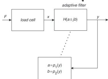
be considered as the parameters of adaptive filter and the relationship between them and the load is expressed in (2) and (3). The adaptive compensation operation is shown in Fig. 2.
Initially the zeros of the filter are set to arbitrary values. Then the outputyis calculated. This new value ofyis used to calculate the zeros of the filter once again. Repeating these steps results in a rapid approach to obtain the steady state value ofy. So far the zeros of the 2nd order compensation filter have been examined. In order that the analogue filter can be realised, it is necessary to add at least two poles to the filter. The values of these poles can be determined practically. These poles are selected as shown in [5]so that the output of the filter quickly reaches its steady-state value with minimum oscillation. The transfer function of the compensation filter is
HðsÞ ¼ ðmþm0Þ s
2þcsþk
105s2þ0:06sþ1 ð4Þ
The transfer functions of the load cell, (1), and its compensation filter, (4), are biquadratic functions. The problem is how to make a biquad adaptive and from a design simplicity point of view, it is necessary to have only one filter component to track changes in m without any influence on the other characteristics of the load cell such as candk. How to achieve this with CMOS transistor-alone circuits is discussed in Section 4 after an introdction to switched-current design, which is given next.
3 Switched-current design principles
The basic element in switched-current (SI) design is a memory cell shown in Fig. 3a. The SI technique exploits the parasitic capacitance,Cgs, at the gate of a MOS transistor to
maintain its drain current[13]. The current memory cell of Fig. 3ahas one transistorM1and three switches, which are
driven by the clock waveforms shown in Fig. 3b and operates as follows. On phasef1, the input current adds to
the bias currentJand the currentJ+iinflows initially into
F F
X
t
t t
Y y
output
input X
sensor filter
P(s)=G(s).H(s)=1 G(s)
G(s) H(s)= 1
Fig. 1 Principle of load cell response correction
load cell x H(a±jb) y adaptive filter
a=p1(y) b=p2(y) F
[image:2.595.332.522.211.350.2] [image:2.595.50.286.311.454.2] [image:2.595.77.284.507.589.2]the discharged gate-source capacitor Cgs. As Cgs charges,
the gate source voltage rises and when it exceeds the threshold voltage,M1conducts. Eventually the whole of the
currentJ+iinflows in the drain ofM1. During the second
phase,f2, the gate ofM1is disconnected from the drain so
the gate voltage is held onCgsand the input switch is now
opened. This forces an output current io¼ iin to flow
[image:3.595.49.285.36.145.2]throughout this phase. The output current is therefore a memory of the input current.
Figure 4a shows a delay cell, created by cascading two memory cells. It should be noted that the output currentio1
is not available through the first phase,f1, and when the
output current is required throughout the entire clock period then another transistor,M3, and its associated bias
current should be added. To achieve a scaled output current, i.e. io2[n]¼aiin[n1], the aspect ratio of M3 is a
times that of M2. This is shown in Fig. 4 by putting ‘1’,
‘1’ and ‘a’ under transistorsM1,M2andM3, respectively,
which means that ½W LM2¼ ½
W
LM1 and ½
W
LM3¼a ½ W
LM2, where W and L are the width and length of the MOS transistors. A switched-current integrator can be obtained by feeding back the output current of the delay cell,io1, to
the input summing node. This results in two parallel switches, one operating withf1and another withf2, which
is equivalent to a short circuit and two parallel bias currents that can be added together. The resulting integrator is shown in Fig. 4b, which can be used as a building block to construct other filter functions[14].
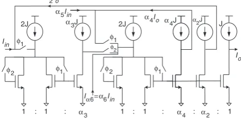
4 Adaptive compensation filter
To simplify the implementation of the compensation filter, we have chosen the integrator-based biquad circuit shown in Fig. 5. With this choice, as shown later in this Section, it is possible to track variation in the load cell measurand by controlling a single filter parameter. This biquad consists of two integrators and two feedback loops (a2Ioanda4Io) and
appropriate signal summations. The s-domain transfer function of the biquad circuit is
HðsÞ ¼
4a6þ2a5a1a3
D
s2þ 4a5
T:D
sþ 4a1a3 T2:D
s2þ 4a4
T:D
sþ 4a2a3 T2:D
ð5Þ
whereD¼2a4a2a3+4,Tis the clock period and eachaiis
the ratio of two currents in the filter circuit. Comparing (5), with the compensation filter transfer function, (4), gives
4a6þ2a5a1a3
D ¼ 10
5ðmþm
0Þ ð6Þ
4a5
T:D ¼ 10
5c ð7Þ
4a1a3
T2:D ¼ 10
5k ð8Þ
4a4
T:D ¼ 600 ð9Þ 4a2a3
T2:D ¼ 10
5 ð10Þ
Equation (6) shows that it is possible to have an adaptive filter, which is capable of tracking variations in m, by controlling only one filter parameter (a6) without any
[image:3.595.310.545.37.152.2]influence on the other characteristics of the filter. Examining Fig. 5 shows that a6 is a coefficient for the filter input
current (Ia6 ¼ a6Iin) and in the adaptive case it should be Ia6 ¼ a6ðmÞIin. In our current-mode filter, the output
current, Io, displays the load cell measurand,m, therefore
having a6 proportional to m is equivalent to control the
filter input current by a variable gain proportional to the filter output current. This means that a current multiplier is needed to make an adaptive compensation filter. This is clarified schematically in Fig. 6.
The design procedure of the compensation filter involves determining the parameters (a1a6) of a fixed filter and then
using a current multiplier block (Fig. 6) to make it adaptive. J
iin
Cgs io
φ1
φ1 φ
1
φ2
φ2
M1
a b
Fig. 3 Current memory cell and clock waveforms aMemory cell
bWaveforms
J J αJ 2J
α
αJ
io iin
iin io2 io1
φ1 φ
1
φ1
φ2
φ2 φ2 φ2
φ2
M1 M2 M3 M1 M2 M3
a b
1 : 1 : 1 : 1 : α
Fig. 4 Delay cell and Integrator aDelay cell
bIntegrator
1 : 1 : α 1 : 1 : : : 1
3
α3J 2J α2J J
2J α4J
α5Iin α2Io
α4Io
Io Iin
α4 α2
Iα6=α6Iin
φ2 φ2
φ2
φ1 φ1
φ1
φ1
Fig. 5 Integrator-based biquadratic filter[14]
adaptive compensation filter
compensation filter sensor output
current multiplier
compensation filter output Io (proportional to m)
Iα6=α6(m)Iin
Iin Iin
Io
[image:3.595.315.548.217.272.2] [image:3.595.363.548.324.454.2] [image:3.595.48.285.521.649.2] [image:3.595.311.548.662.754.2]From experimental data for a particular load cell [2] the damping factorc, spring constantk, and the effective mass of the load cellm0, are 3.5, 2700 Pa, and 0.1 kg, respectively.
In addition, as a starting point,mis considered to be 1 kg, which is an arbitrary choice. The parameters of the compen-sation filter can be calculated using (6)–(10). As outlined earlier, the filter parameters,ai, are implemented byWL of the
transistors in the current mirrors. The clock period, T, affects the spread of the transistor sizes for the filter. For different clock periods, considering (4) as the transfer function of the compensation filter results in wide ranges for
ai, which seems impractical. In order to achieve reasonable
W
L for the transistors in the filter design, the positions of filter poles in (4) are changed and scaled in magnitude. Note that the filter poles do not have a significant effect on the compensation (refer to Section 2). Therefore, the modified transfer function for the compensation filter is
HðsÞ ¼ 1 2700
ðmþm0Þ s2þcsþk
ð4104Þs2þ0:035sþ1 ð11Þ
With this transfer function, choosingT¼102s provides parameter spread of 25 : 1, while for T¼105s it is 3 000 000 : 1, which is clearly impractical. It is worth noting that the load cell output is oscillatory with low frequency (less than 30 Hz), therefore T¼102s is a reasonable choice. Using the values in the modified transfer function, (11), in (6)–(10) gives the parameters of the compensation filter shown in Table 1.
Load cell response correction for different values of the measurand, m, requires changing the compensation filter zero positions. As discussed earlier in this Section, this can be achieved simply by varying the value of the parametera6
of the filter. To find howa6is related tom, using (6)–(10),
the parameters of the filter are calculated for different values ofmfrom 0.1 kg to 1 kg. It is seen that the parametersa1to
a5have the same values as in Table 1, but the value ofa6
differs for eachm, as shown in Table 2.
It is possible to express the table values as a linear relationship betweena6andm
a6¼1:4816mþ0:074 ð12Þ
To ensure the correct operation of the transistors in the filter circuit, it is assumed that a load cell measurand of m¼1 kg corresponds to 10mA output current. Therefore, with reference to Fig. 6 and using (12), to have an adaptive compensation filter, a current multiplier block with the following relationship between its input and output is required
Ia6¼a6Iin¼ ð0:14816Ioþ0:074Þ Iin ð13Þ
whereIin is input to the filter (output of the sensor),Ia0 is output of the filter and Ia6 is the current required for the
second integrator in the filter (Fig. 5). The implementation of (13) with CMOS transistors is discussed next.
4.1
Proposed current multiplier for
adaptive compensation
One approach to achieve multiplication of two signals x and y is accomplished by evaluating their quadratic terms: ðxþyÞ2 ðxyÞ2 ¼ 4xy. With this base, in[15] a CMOS current gain cell is proposed. The principle of operation of this current gain cell is shown in Fig. 7. It consists of a summer and subtractor (S & S), a linear current to voltage convertor, and two matched MOS tran-sistorsM1andM2, which are assumed to be in saturation
region and each performs voltage-to-current conversion with a squaring characteristic. I1is the input current to be
amplified andIcis a current for the gain control. These two
currents are applied to the input nodes of S & S. Afteri!v conversion, both voltages, R(Ic+I1) and R(IcI1) are
applied to M1 and M2, respectively (R is the conversion
factor). Applying a square-law characteristic toM1andM2
yields
Iom¼ILIR¼b
2½RðIcþI1Þ VT
2b
2½RðIcI1Þ VT
2
¼2bRðIcRVTÞI1 ð14Þ
where Iom is the output of the current gain cell and b¼mCoxW/L,m is the mobility of carriers,Cox is the gate
capacitance per unit area, VTis the threshold voltage, and WandLare the channel width and length of the devices, respectively.
To evaluate this current gain cell, transistor level simulation was performed using Cadence with 0.35mm 3.3 V BSim3v3 CMOS foundry models. The following linear relationship of the cell input-output was obtained empirically
Iom¼0:087ðI1þ33ÞðIcþ0:263Þ
for: 8oI1o55mA and 0:2oIco8mA ð15Þ
Out of the above ranges forI1andIc, there is a nonlinear
[image:4.595.61.551.511.758.2]input-output relationship because some of the transistors in the S & S are leaving their saturation region. Whereas, for
Table 1: Compensation filter parameters,T¼102s
a1 a2 a3 a4 a5 a6
1 1 0.4 1.4 0.0519 1.556
Table 2: Filter parameter a6 for different values of measurand
m(kg) 0.1 0.2 0.3 0.4 0.5 0.6 0.7 0.8 0.9 1
a6 0.222 0.37 0.519 0.667 0.815 0.916 1.111 1.259 1.407 1.556
IL
Ic
Ic + I1
Ic − I1 i M1 M2
IR
I1
S & S v
R(Ic + I1) R(Ic − I1)
[image:4.595.46.551.739.771.2]the adaptive compensation filter, a current multiplier with the following features is needed:
1. Input-output relationship of (13)
2. If we consider that the compensation filter operates for 0omo1 kg, then the range of multiplier input currents should be 0oIino20mA and 0oIoo10mA. It should be noted that 10mA current corresponds to m¼1 kg and since the load cell output (Iin) is oscillatory, with the
steady-state value of 10mA, its peak could be as much as 20mA.
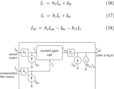
To achieve these two features, the block diagram depicted in Fig. 8 is proposed, which contains current mirrors (b1,bc
and bo), constant current sources (I01, I0c and I0o) and a
dependent current source (b11Iin). The aim of b1 and
constant current sourcesI01andI0care to bring the range of
the multiplier input currents to the operating range of the current gain cell. The following equations can be obtained from Fig. 8
I1 ¼ b1IinþI01 ð16Þ
Ic ¼ bcIoþI0c ð17Þ
Ia6 ¼ boIomI0ob11Io ð18Þ
Combining (16), (17), (18) and (15) yeilds
Ia6 ¼0:087bob1bcIoIin
þ0:087bob1ðI0cþ0:263ÞIin þ½0:087bobcðI01þ33Þ b11I0
þ0:087boðI01þ33ÞðI0cþ0:263Þ I0o ð19Þ
Equation (19) should be made equivalent to (13), which gives the appropriate values for bc, b0,b11 andI0o.
This is achieved by making the coefficients ofIoIinand Iin
in (19) equal to the coefficients of IoIin and Iin in (13),
respectively and making the third and fourth terms of (19) equal to zero, because there is no constant term and a term proportional to Ioin (13). The CMOS realisation
of the block diagram of Fig. 8 is shown in Fig. 9. The size of squaring characteristic transistors, M1 and M2
are equal and it isW
L ¼
100mm 10mm and
W
L of transistors ini!v convertors are 103mmmm. The other part of the circuit, inclu-ding S & S, are composed of current mirrors. The structure of the current mirrors and the size of their transistors are designed such that to be compatible with the the compensation filter, which is explained in the next Section. With this circuit, it is possible to realise (13) for 0oIino20mA and 0oIoo10mA.
4.2
CMOS adaptive compensation filter
The biquadratic filter of Fig. 5 contains bias current sources and switch symbols, which need to be replaced by transistor designs to allow CMOS implementation of the circuit. Furthermore, the biquad has memory cells and current mirrors as outlined in Section 3. Current mirrors and memory cells affect the performance of switched-current circuits and numerous designs have been proposed to have improved cells [14]. In this work, to improve transmission errors, owing to the finite input conductance and nonzero output conductance of transistors, high compliance cascode memory cell and current mirror have been used. The bias currents for the memory cells and NMOS mirrors are chosen to be J¼100mA, which are provided by PMOS compensationfilter output sensor output
current gain
cell (refer to fig.6)
Iin
Io
Ic
bc b1
b11Io bo
I0o
Iα6
I
om
I0c I01 I1
Fig. 8 Proposed multiplier block diagram to achieve adaptive compensation
S & S
90
90 90
90 90 90 90 90
90
90 90
90
90 90 30
30 55
55
30
30 30 30 30
30 30 30 30
30 30 60
60 30
30 30
90 90
10 10
10 10 10
10
100 100 30 30 30
28
28
30
30 30 90 89.85
89.85
308.1
308.1
103
103 90
90
90 90
90 90
90
90 86.2
86.2
90 90 90
90
90 180
180 157.8
157.8
3 3 3 3 3 3 3 3
3
3
3 3 3 3 3 3
sensor output
3 3
3 3
3 3 3
3 3 3
3
3 3
3
3 3
3 3
(refer to fig.6)
3 3 3 3
3
2
2 2
2
2 2
2 2 2
2
2 2 2
2 2 2 2
2 2
2 2
2 2
2 2 2 2 2
2 2 2 2 2
2 2
Io
Iom= IL−IR
Iα6 Iin
VbiasCN
VbiasCN VbiasCP VbiasP
VbiasCN VbiasCP
VbiasP
compensation filter output
1
1 1 1
b1
b11
M1M2
1 bo
bc
v i
[image:5.595.51.285.255.436.2] [image:5.595.61.537.493.751.2]mirrors of the same type and bias voltages (VbiasP, VbiasCP
andVbiasCN) can be produced by a separate bias generation
circuit once and distributed to all the current mirrors in the design[16]. Different bias currents in all the current mirrors can be altered easily by scaling all transistor widths. In addition, the circuit needs to be preceded by a sample-and-hold with multiple scaled output currents, which provide the parametersa1,a5and the input of the current multiplier. All
the filter switches are implemented by NMOS transistors. The complete adaptive compensation filter is shown in Fig. 10, in which the box marked ‘X’ denotes the proposed multiplier circuit of Fig. 9 needed to achieve adaptive operation. As it can been seen, the adaptive compensation filter consists entirely of transistors without using capacitors and resistors, which retains the important advantage of being compatible with digital CMOS process.
The combination of relatively large size memory transistor and minimum geometry switch transistor is chosen primarily to keep the effect of charge injection errors at a reasonable level. However, the use of a reasonably large memory transistor also has other perfor-mance benefits, such as lower output conductance, better matching and improved current mirror resolution, which need to be balance against the speed advantage of small devices. Hence, the aspect ratio of the memory transistors is considered to beW
L ¼
30mm
3mm and for the NMOS
W
L¼
2mm 0:35mm.
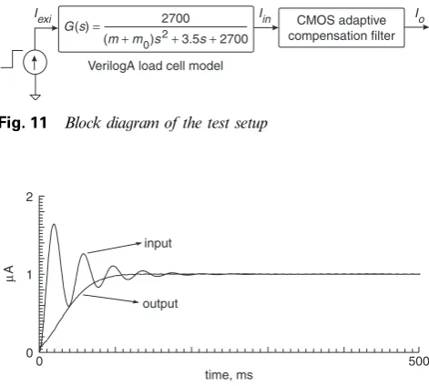
5 Test and results
To test the compensation filter, the output signal of the load cell is needed. In[4], we developed computer models for the load cell and the adaptive compensation filter and they have been implemented in PSpice, and also validated by practical discrete circuit [5]. However, for CMOS transistor level simulation with Cadence, a VerilogA behavioural modelling facility has been used, which can produce load cell oscillatory current. A step excitation current is applied to the load cell model (Fig. 11) whose output has been applied to the compensation filter and according to the amplitude of excitation current, the value of the (m+m0) has been
changed in the VerilogA model.
The circuit in Fig. 10, including the multiplier circuit of Fig. 9, was simulated using Cadence with 0.35mm 3.3 V BSim3v3 CMOS foundry models. Figure 12 shows the load cell output and the compensation filter output for m¼0.1 kg, which corresponds to 1mA excitation current. To illustrate the capability of the filter in tracking changes VbiasP
VbiasCP
VbiasCN Iin
Iin Io
Io sensor
output adaptive
filter output
dump
dump
φ1
φ1
φ1
φ1 φ2
φ2
φ2
φ2
φ2
φ1
φ1
α5 α1 1 1 α3 1 1 α4 α2 1 1
1 1 1 1
90 90 90 90 4.68 90 90 90
4.68
36
36
90 90 90
90 90
90 90 90 90
90 90 90
90 90
90 90 90
3
2 2 2 2
6
2
2 2 2 2
3 3 3
3 3 3
3 3
3
3 3
3 3 3
3
2 2
2
2 2 2 2
2
2 2 2
2 2 2
2 2 2 2 2
2 2 2
2 2
6
6 0.35 0.35
30
30
30 30 30 30 30
30 30
30 30 30 30
30 30
30 30 30
30
30 30
30 30
30 1.56 0.35
2 2
3 3 3 3 3 3 3 3 3 3 3 3 3 3
1.56 0.35
42
42 12
6 0.35
126
0.35 0.35
0.35 0.35
12
126
[image:6.595.60.538.32.260.2]Iα6
Fig. 10 Adaptive compensation filter containing only CMOS transistors
Iexi Iin Io
VerilogA load cell model
CMOS adaptive compensation filter 2700
G(s) =
[image:6.595.311.547.382.594.2](m + m0)s2+ 3.5s + 2700
Fig. 11 Block diagram of the test setup
0 0
500 input
output 2
1
µ
A
time, ms
Fig. 12 Input and output of the adaptive compensation filter for m¼0.1 kg
0 500
input
output 6
3
0
µ
A
[image:6.595.315.544.648.747.2]time, ms
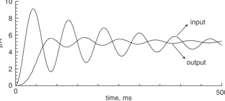
inm, Figs. 13 and 14 show the results for m¼0.3 kg and m¼0.5 kg corresponding to 3mA and 5mA excitation current, respectively. Clearly these results show that fully CMOS adaptive compensation filter can be used to correct the oscillatory output of the load cell. To indicate the effectiveness of using an adaptive filter, a fixed filter was also used for compensation. When the excitation current is 5mA, a fixed filter suitable for m¼0.1 kg have been used and the input and output of the filter are depicted in Fig. 15, which shows that the fixed filter is unable to perform the sensor response correction.
6 Concluding remarks
This paper has shown that it is possible to perform effective response compensation of dynamic sensors using switched-current techniques. The proposed analogue adaptive filter employs only transistors without using passive elements and therefore compatible with digital CMOS processing, which makes it suitable for system-on-chip applications. This has been demonstrated with a reference to a load cell sensor. It
has been shown that the integrator-based biquadratic filter provides an accurate and flexible compensation filter model, since it needs only one filter parameter to track variations in the load cell measurand. Adaptive response correction is achieved by developing a new CMOS current multiplier circuit. Transistor-level simulations of the adaptive com-pensation filter, with realistic Spice transistor models, confirm the effectiveness of the proposed technique.
7 References
1 Shi, W.J., White, N.M., and Brignell., J.E.: ‘Adaptive filters in load cell response correction’, Sens. Actuators A, 1993, A 37–38, pp. 280–285
2 Yasin, A.A., and White, N.M.: ‘The application of artificial neural network to intelligent weighing systems’, IEE Proc., Sci., Meas. Technol., 1999,146, pp. 265–269
3 Shu, W.-Q.: ‘Dynamic weighing under nonzero initial condition’, IEEE Trans. Instrum. Meas., 1993,42, (4), pp. 806–811
4 Jafaripanah, M., Al-Hashimi, B.M., and White, N.M.: ‘Load cell response correction using analog adaptive techniques’. IEEE Int. Symp. on Circuits and Systems, Thailand, May 2003, pp. IV75275–5 5 Jafaripanah, M., Al-Hashimi, B.M., and White, N.M.: ‘Application of analog adaptive filters for dynamic sensor compensation’, IEEE Trans. Instrum. Meas., 2005,54, (1), pp. 245–251
6 Graupner, A., Schreiter, J., Getzlaff, S., and Schuffny, R.: ‘CMOS image sensor with mixed signal processor array’,IEEE J. Solid-State Circ., 2003,38, (6), pp. 948–957
7 Sergio, M., Manaresi, N., Campi, F., Canegallo, R., Tartagni, M., and Guerrieri, R.: ‘A dynamically reconfigurable monolithic CMOS pressure sensor for smart fabric’, IEEE J. Solid-State Circ., 2003,
38, (6), pp. 966–975
8 Chatzandroulis, S., Goustouridis, D., Normand, P., and Tsoukalas, D.: ‘A solid-state pressure-sensing microsystem for biomedical applications’,Sens. Actuators A, 1997,62, pp. 551–555
9 Kawahito, S.: ‘Recent developments in sensor interfaces’. EURO-SENSORS XVI, Czech Republic, Sept. 2002, pp. 37–40
10 Rubio, C., Bota, S., Macias, J.G., and Samitier, J.: ‘Modelling, design and test of a monolothic integrated magnetic sensor in a digital CMOS technology using a switched current interface system’,Analog Integr. Circuits Signal Process., 2001,29, pp. 115–126
11 Hughes, J.B., Worapishet, A., and Toumazou, C.: ‘Switched-capacitors versus switched-currents’. IEEE Int. Symp. on Circuits and Systems, Switzerland, May 2000, pp. 409–412
12 Rubio, C., Ruiz, O., Bota, S., and Samitier, J.: ‘Switched current interface circuit for micromachined accelerometer’. IEEE Instrumen-tation and Measurement Technology Conf., May 1999, pp. 458–463 (Italy)
13 Hughes, J.B., Bird, N.C., and Macbeth, I.C.: ‘Switched-current, a new technique for analogue sampled-data signal processing’. IEEE Int. Symp. on Circuits and Systems, May 1989, pp. 1584–1587
14 Toumazou, C., Hughes, J.B. and Battersby, N.C. (Eds.) ‘Switched-current: an analogue technique for digital technology’ (IEE Peter Peregrinus Ltd., London, UK, 1993)
15 Wang, Z.: ‘Two CMOS large current-gain cells with linearly variable gain and constant bandwidth’,IEEE Trans. Circuits Syst. I, Fundam. Theory Appl., 1992,39, (12), pp. 1021–1024
16 Wilcock, R., and Al-Hashimi, B.M.: ‘Power-aware design method for class A switched-current wave filter’,IEE proc., Circuits Dev. Syst., 2004,151, (1), pp. 1–9
0 500
input
output 2
4 6 8 10
0
µ
A
[image:7.595.52.288.36.134.2]time, ms
Fig. 14 Input and output of the adaptive compensation filter for m¼0.5 kg
0 500
input
output 2
4 6 8 10
0
µ
A
time, ms
[image:7.595.54.281.186.288.2]