Evolution of the
m‑
Plane Quantum Well Morphology and
Composition within a GaN/InGaN Core
−
Shell Structure
Pierre-Marie Coulon,
*
,†Shahrzad hosseini Vajargah,
‡An Bao,
‡Paul R. Edwards,
§Emmanuel D. Le Boulbar,
†Ionut Girgel,
†Robert W. Martin,
§Colin J. Humphreys,
‡Rachel A. Oliver,
‡Duncan W. E. Allsopp,
†and Philip A. Shields
††Department of Electronic and Electrical Engineering, University of Bath, Bath BA2 7AY, U.K.
‡Department of Materials Science and Metallurgy, University of Cambridge, Cambridge CB3 0FS, U.K.
§Department of Physics, SUPA, University of Strathclyde, Glasgow G4 0NG, U.K.
*
S Supporting InformationABSTRACT: GaN/InGaN core−shell nanorods are promising for optoelectronic applications due to the absence of polarization-related
electric fields on the sidewalls, a lower defect density, a larger emission
volume, and strain relaxation at the free surfaces. The core−shell
geometry allows the growth of thicker InGaN shell layers, which would
improve the efficiency of light emitting diodes. However, the growth
mode of such layers by metal organic vapor phase epitaxy is poorly understood. Through a combination of nanofabrication, epitaxial growth, and detailed characterization, this work reveals an evolution in the growth mode of InGaN epitaxial shells, from a two-dimensional (2D) growth
mode to three-dimensional (3D) striated growth without additional line defect formation with increasing layer thickness.
Measurements of the indium distribution show fluctuations along the <10−10> directions, with low and high indium
composition associated with the 2D and 3D growth modes, respectively. Atomic steps at the GaN/InGaN core−shell interface
were observed to occur with a similar frequency as quasi-periodic indiumfluctuations along [0001] observed within the 2D layer,
to provide evidence that the resulting local strain relief at the steps acts as the trigger for a change of growth mode by elastic
relaxation. This study demonstrates that misfit dislocation generation during the growth of wider InGaN shell layers can be
avoided by using pre-etched GaN nanorods. Significantly, this enables the growth of absorption-based devices and light-emitting
diodes with emissive layers wide enough to mitigate efficiency droop.
I
nGaN alloys and more generally III-nitride materials havebeen widely studied since their successful application in blue light-emitting diodes (LEDs) and laser diodes (LDs) in the
early 90s.1With the possibility to tune the wavelength emission
from 3.4 eV for GaN, to 0.7 eV for InN, InGaN quantum wells have been employed to achieve UV, blue, green, and white
LEDs2,3 and used for solar cells4,5or for water splitting.6,7
Despite commercialized devices with efficient near band edge
emission, InGaN heterostructures grown on two-dimensional
(2D) GaN layers still suffer from limitations such as poor
crystalline quality due to the large lattice mismatch,8,9difficulty
in growing high indium content layers,10,11 pre-existing
threading dislocations that adversely affect LED/LD
perform-ance,8and the introduction or expansion of V-defects and pits
in the epitaxy.8,9,12The growth of thicker InGaN layers on GaN
(or AlGaN) can lead to phase separation,11,13plastic relaxation,
and elastic relaxation.14,15The result is the generation of new
dislocations and three-dimensional (3D) growth that directly
impact the InGaN emission properties.8,9,16−18 Additionally,
thick InGaN layers grown with the conventional c-plane
orientation are seriously impacted by the quantum-confined
Stark effect (QCSE), which results in poor emission efficiency
due to the large spatial separation between electron and hole wave functions. The alternative of growing InGaN layers on the nonpolar and semipolar planes of wurtzite GaN to avoid the QCSE usually results in the formation of high densities of
stacking faults that compromise the emissive properties,19,20
unless grown on bulk GaN.
One way of circumventing these problems is to use a nanorod (NR) geometry that incorporates radial or axial InGaN heterostructures. Compared to 2D layers, GaN NRs
allow an efficient strain relaxation21and can provide an almost
defect-free core,22 opening the possibility of higher indium
incorporation with lower defect density, especially in the axial
configuration.23,24In core−shell structures, InGaN growth on
the nonpolar NR sidewalls not only eliminates the
polarization-related electricfields but also leads to a larger emission volume
for a given substrate footprint.25These advantages, as well as
the potential to improve light extraction efficiency and
Received: August 29, 2016 Revised: December 22, 2016 Published: January 3, 2017
Article
pubs.acs.org/crystal License, which permits unrestricted use, distribution and reproduction in any medium,
provided the author and source are cited.
Downloaded via UNIV OF STRATHCLYDE on November 21, 2018 at 13:40:26 (UTC).
reabsorption, have therefore stimulated global interest in GaN/
InGaN NR LEDs26,27and solar cells.28
The main focus of the GaN/InGaN core−shell literature to
date has been on structures in which the InGaN layers are just
2−5 nm thick,25,29−32 similar to the thicknesses of single or
multiquantum well structures grown onc-plane GaN. However,
the carrier densities in such narrow wells are high under normal
LED operating conditions, with the consequence that efficiency
droop is large. A particular motivation of this work is to grow and characterize wider InGaN layers on the nonpolar surfaces
of core−shell structures in order to determine the scope to
grow thicker active layers in GaN-based NRs for optoelectronic applications. The increase in the emissive volume of LEDs will
have the effect of reducing the average carrier density in the
emissive region for a given injection current and thus
significantly mitigate efficiency droop.
Relevant work to date on GaN/InGaN core−shell NRs has
focused on the optical uniformity of a wide (10 nm) InGaN
single quantum well (SQW) on m-plane sidewalls, revealing
nanoscalefluctuations in the InN mole fraction of up to 2.0−
2.5 atom %.33 This paper focuses on the evolution of the
nanoscale fluctuations with increasing InGaN layer thickness,
correlating changes in the nanoscale morphology with the local
indium content. It is shown that m-plane miscut and related
atomic layer steps in the faceted NR sidewalls can induce large
fluctuations in the indium content and the morphology of
nominally pseudomorphic InGaN thin films on a nanometer
length scale. The results reveal wider implications for the growth of multicomponent alloy pseudomorphic epitaxial layers
in core−shell structures and on their applications in
optoelectronics.
■
RESULTS AND DISCUSSIONThe InGaN shell layers used for this study were all grown on
etched GaN NR arrays with a pitch of 2 μm, obtained by
etching a GaN 2D layer down to the silicon substrate.34 The
use of top-down etching and regrowth gives rise to high
uniformity of the NR array.35,36 First, a metal organic vapor
phase epitaxy (MOVPE) GaN regrowth step was performed to
recover them-plane and semipolar plane facets on the etched
NR arrays. Next, an InGaN layer was grown underfixed growth
conditions for a duration of 2, 6, or 18 min. A second set of three identical structures was grown, but this time with a GaN
capping layer grown at 850 °C to create an InGaN/GaN
double heterostructure. Further details of the overall NR
fabrication process can be found in theExperimental Section
[image:2.625.93.539.67.291.2]andSupporting Information.
Figure 1displays the evolution of the NR morphology as a function of the InGaN growth time. In each case the NR is
defined by an envelope comprising six {10−10}m-plane facets,
six {1−101} semipolar facets, and a truncated top (0001) c
-plane facet. The high magnification scanning electron
microscopy (SEM) images (Figure 1d,f) reveal a nanoscale
evolution in the morphology of them-plane facets with growth
time. After 2 min growth the uncapped InGaN layer grown on
the m-plane appears smooth without apparent roughness or
change in morphology. After 6 min growth, surface roughness
clearly appears along the entire length of them-plane, with line
features running parallel to the c-plane. After 18 min growth,
these linear features are clearly revealed to be striations (Figure
1f). The same trend is observed when a GaN capping layer is
grown over the InGaN layer.
For 18 min InGaN growth, cross-section (Figure 1f) and
plan-view (inset in Figure 1c) SEM pictures clearly show a
higher growth rate along the <11−20> direction, without {11−
20} facets developing, compared to the <10−10> direction,
indicating that group III species are preferentially incorporated
on the edges between adjacent m-plane facets. The higher
growth rate observed along <11−20> is likely due to the strain
relaxation that occurs at the edges, enabling the larger indium
atoms to be incorporated with less lattice dilation.37
The change in m-plane surface morphology observed as a
function of the InGaN shell growth time was further examined by atomic force microscopy (AFM) experiments on NRs deposited onto a bare Si substrate by a scratching method. In addition, GaN faceted NRs (also referred to as 0 min InGaN)
Figure 2.300×200 nm2AFM scan of them-plane for (a) GaN faceted NR (image height (h) = 2 nm), (b) 2 min (h= 2 nm), (c) 6 min (h= 3 nm), and (d) 18 min (h= 10 nm) uncapped InGaN shell growth time. AFM scans have been used to extract the RMS value of them-plane avoiding any contribution of the edges. AFM line scans are traced along thec-axis to compare the height and spacing of the features or striations (e) in the middle of them-plane as a function of the InGaN shell growth time and (f) between the middle of them-plane and the edges for 18 min InGaN.
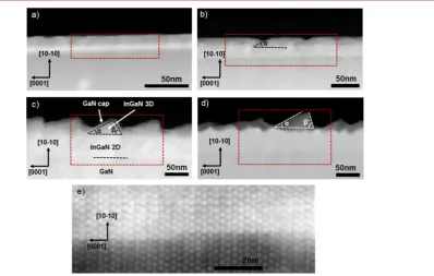
Figure 3.TEM pictures recorded along the [11−20] zone axis of GaN/InGaN core−shell structures grown by MOVPE with a GaN capping layer for (a) 2 min, (b) 6 min, (c) 18 min InGaN growth, and (d) for 18 min uncapped InGaN. The red dashed rectangle indicates the area where EDX spectra were acquired. The angleα= 29±1°corresponds to the average angle relative to them-plane of the facet pointing toward [0001], whereasβ = 51±1°andβ′70±1°correspond to the different angles relative to them-plane of the facet pointing toward [000−1]. (e) HRTEM picture of the
[image:3.625.133.532.425.678.2]were also characterized to assess the initial surface morphology
of the GaN m-plane sidewall. The RMS roughness value for
each sample is extracted from the center of them-plane (300×
200 nm2) to avoid any contribution of the edges.
The AFM height image of the GaN m-plane facet (Figure
2a), prior to the InGaN growth, exhibits quasi-periodic shallow
step-like features running parallel to the a-axis with an RMS
roughness of 0.184 nm. After 2 min InGaN growth (Figure 2b),
similar features can be observed with a slightly increased roughness of 0.212 nm. With further growth, these linear
features grow in height (i.e., along the <10−10> or m
-direction) leading to the formation of striations and an increase
in the RMS roughness to 0.403 nm for 6 min (Figure 2c) and
1.03 nm for 18 min (Figure 2d).
The initial quasi-periodic spacing of 20−40 nm between the
step-like features observed for 0 min remains the same for longer InGaN growths up to the 18 min sample where merging/coalescence and local misalignment of the striation line features leads to an increase in the spacing, especially at the
intersections of them-planes where the spacing can reach up to
100 nm as the striations merge into larger structures (Figure 2f
andFigure S2dof the Supporting Information). This is due to the faster growth rate and higher indium incorporation at these positions.
AFM line profiles are used to extract the height of the
step-like features and striations from the middle of them-plane facet,
along thec-axis (see further details inFigures S2 and S3of the
Supporting Information) and are shown inFigure 2e for the
various InGaN growth times. Measurements of the heights of the observed steps in AFM for the GaN faceted NR indicate that the vast majority consist of a single monolayer (ML) of
GaN on them-plane facet (seeFigure S3). Then, as a function
of the InGaN growth time, an increase in the height distribution size can be observed, up to 10 nm for the thickest
InGaN in the middle of the m-plane facet, and up to 20 nm
close to the edges (Figure 2f).
The features observed on the m-plane sidewalls of GaN
faceted NRs are unambiguously ascribed to the presence of meandering steps. The fact that the size and the periodicity of these features remain the same after 2 min InGaN growth means that the initial InGaN layer formation occurs via a 2D
step-flow growth mode. For longer growth, the change in size,
alignment, and periodicity of the striations indicate that a
significant perturbation at the surface takes place between 2 and
6 min InGaN growth, which is then exacerbated by continuing the InGaN growth to 18 min.
The surface morphology of the m-plane facet of the three
InGaN capped samples and the 18 min InGaN uncapped sample was assessed by transmission electron microscopy
(TEM), and the results are presented inFigure 3. In agreement
with SEM and AFM observation, a change in morphology of
the m-plane InGaN is observed with increasing growth time,
from appearing essentially smooth for a 2 min growth time, evolving to a clearly roughened and striated surface after 18 min InGaN growth. Additional TEM color pictures recorded along
the wholem-plane for the samples studied are shown in Figure
S4 of the Supporting Information. The GaN capping layer
(grown for 5 min) is conformal with the InGaN and has the same morphology and roughness. The increase of roughness with growth time seen on the SEM and AFM data can be correlated in the TEM images: the striations observed in the
SEM and AFM images for the 6 min InGaN growth inFigures
1b and 2c are associated with the formation of new inclined
facets that delineate sharply defined prismatic structures after
18 min InGaN growth (Figure 3c,d). After 6 min InGaN
growth, the facets of the striation match to anm(1−101) plane
(α in Figure 3b,c), whereas after 18 min, the facet pointing
toward [000−1] gradually evolves to a (11−24) or (1−105)
plane (respectivelyβandβ′inFigure 3c,d).
An estimation of the InGaN SQW thickness can be obtained
from the difference in GaN and InGaN contrast in the TEM
images along the [10−10] direction, being 8±1 nm and 20−
24±1 nm for the 2 and 6 min growth, respectively. Because of
the emergence of the new facets after 6 min, the interface between the InGaN SQW and the GaN capping layer is no
longer sharp, which leads to a thickness variation along them
-plane. In the case of the 18 min growth, an additional change in
contrast along the [10−10] direction allows two layers to be
distinguished: a bright two-dimensional (2D) layer having a
thickness of 50 ± 2 nm and a dark three-dimensional (3D)
striated layer having a variation in thickness up to 40−45 nm
(Figure 3c,d) that compare well with the height and periodicity
of the striations observed by AFM on the edges (Figure 2f).
Compared to the 18 min capped growth, its equivalent
uncapped sample (Figure 3d) has two distinct types of
striation: 5−10 nm high undulations separated by 25−50 nm
(bright contrast) and 30−45 nm high undulation with a 50−
100 nm spacing. Thus, the TEM images involve not only the
morphology of the m-plane but also the morphology of the
edges.
An additional change in contrast can also be observed along
thec-direction, within the InGaN 2D layer for all three InGaN
growth times, but most noticeably in the 6 and 18 min grown
samples (see also Figure S4b−d of the Supporting
Information). Narrow darker regions inclined at 41 ± 2°
((11−23) plane) to them-plane occur quasi-periodically. Since
this change in contrast is observed only within the InGaN layer, it is not an artifact of the TEM preparation; rather, it is related
to a real variation in them-plane InGaN growth. These features
will be discussed later after the determination of the indium composition within these layers.
No generation of defects (i.e., misfit dislocations or basal
stacking faults) has been observed within the SQW in the NRs studied irrespective of the growth time. Complementary high-resolution TEM pictures have been performed at the GaN/ InGaN interface and highlight the presence of atomic steps at
the GaN/InGaN interface (Figure 3e), in agreement with the
AFM observations on GaN faceted NRs (Figure 2a), but do not
show the presence of misfit dislocations along the m-plane
facet.
The formation of atomic steps on them-plane facets of GaN
NRs can be explained through understanding the fabrication process of the NRs. After the etching step that leads to the formation of the NRs, the lateral sidewalls of the NRs are slightly tapered; i.e., there is a small decrease of diameter from
the bottom to the top.35 While the GaN regrowth step will
eventually reveal the slowest growing planes, such as the m
-plane, the presence of atomic steps at the GaN/InGaN interface suggests that the recovery is not complete, leading to a
+c m-plane miscut of 0.4±0.01°(see further details on miscut
calculation in Figure S3 of the Supporting Information).
Detailed analysis of SEM data on similar samples reveals the
same conclusion.35
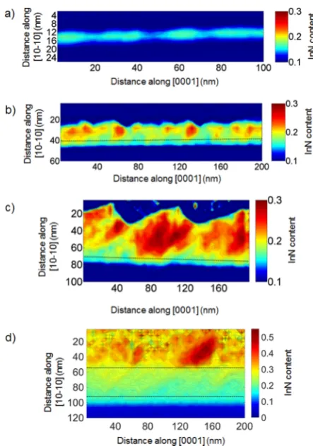
on them-plane facets for the InGaN-capped samples grown for 2, 6, and 18 min and the 18 min InGaN uncapped sample. Note that the color scale bar used for the EDX maps of the capped
InGaN samples corresponds to a 10−30% variation in InN
mole fraction content, whereas a 0−50% InN mole fraction
scale bar was used for the uncapped InGaN sample. A clear increase in the volume averaged indium composition and its inhomogeneity can be seen with the increase in growth time. For each capped sample a maximum InN content of the InGaN
layer has been calculated: 15% ±2% for 2 min growth time,
25%±2% for 6 min, and 30%±2% for 18 min. Since all other
growth parameters were kept constant, it can be inferred that
the increase in InN content and itsfluctuations in the InGaN
layers derives solely from the transition from a quasi-2D to a 3D growth mechanism.
Focusing on the InNfluctuations, after 2 min InGaN growth
(Figure 4a), EDX maps reveal quasi-periodical lateral
fluctuations along the c-axis, with a difference in InN content
of 2−3% and an average spacing of∼20 nm between high and
low InN content within the 8 nm wide InGaN SQW. The good correlation found between the quasi-periodicity of atomic steps
observed on GaN facets along thec-axis in AFM (Figure 2a)
and the quasi-periodical InNfluctuations detected along thec
-axis after 2 min InGaN (Figure 4a) supports the assumption
that the presence of atomic steps triggers InN fluctuations
within the SQW. Indeed, atomic steps can enable the local accommodation of stress in pseudomorphic InGaN epitaxial layers by providing sites for preferential indium incorporation, either at the step itself due to the greater scope for bond
relaxation38,39or by introducing a species-dependent Ehrlich−
Schwöbel barrier (ESB) that inhibits, for example, theflux of In
atoms perpendicular to the steps in the growing surface.40Since
the InGaN growth adopts a step-flow growth mode between 0
and 2 min, as indicated by AFM characterization, it follows that after the deposition of each InGaN monolayer, preferential incorporation of indium will occur at or near the step edge, where the inherent strain induced due to the large atom size can be relaxed by displacing its lattice site. This is similar to what is observed in InGaN planar growth where it is suggested that adsorbed indium atoms migrate to the dilatational strain
field of a dislocation core,41or more generally, that the kinetic
mechanism of inhomogeneity formation is coupled to surface
morphology.42
With the increase of growth time to 6 min (Figure 4b), two
InGaN layers can now be distinguished along the [10−10]
direction: first, a continuous inner layer of 8 nm of relatively
[image:5.625.67.289.64.380.2]homogeneous InN content (delineated by a dashed line in Figure 4b), and with a InN fraction of ∼15% similar to that observed after 2 min; and second, an outer layer characterized
by lateral fluctuations in InN content of 10% with faceted
regions of InN content up to 25%. The InNfluctuations again
occur quasi-periodically with an average spacing of 20 nm. It is striking that the average lateral spacing of the InN content after 6 min is not only in good agreement with the striation spacing
observed in AFM, but also similar to the lateral InNfluctuation
average spacing estimated after 2 min. It is very likely that the
high and low InN content variation of 2−3% seen after 2 min
InGaN growth has created a sufficient perturbation, via elastic
strain relaxation, to initiate the nucleation of others facets on
the m-plane. Such facets, which look like islands for 6 min
growth, will lead to a relaxed area where a favorable binding of
indium atoms occurs,17,18,38,42 explaining the higher indium
content of the outer faceted InGaN layer compared to the inner
layer. In InGaN c-plane growth the formation of 3D islands,
occurring via elastic strain relaxation, will induce higher indium incorporation, particularly near the top of the island where the material is the most relaxed, leading to high indium
fluctuation.17,18The growth mode commonly ascribed to the
formation of 3D islands or nanostructures such as quantum
dots is the Stranski−Krastanov (SK) growth mode wherefirst, a
2D pseudomorphic strain layer with a low indium content due
to the strain compositional pulling effect is grown,16followed
by 3D elastically relaxed growth favorable to higher indium
incorporation. In the present case, afirst layer with low indium
content is observed, followed by the formation of a 3D striated layer composed of new facets, with higher indium content. As
such, the InGaN growth mode on the m-plane facets of the
fabricated NRs is similar to SK growth, except for being triggered by atomic layer steps. Unlike the nucleation of a 3D
island geometry inc-plane growth of InGaN/GaN QWs, which
is mainly due to the existence of a biaxial strain, the presence of atomic steps leads to the formation of 3D striations
preferentially aligned along thea-axis.
As growth proceeds, there is a competition between the
remainingm-plane and other facets. After 18 min, well-defined
facets other than them-plane are obtained, indicating that the
growth proceeded via a self-limiting process, with them-plane
growing faster than the (1−101) and (11−24) or (1−105)
facets. Similar to that observed after 6 min, the EDX map (Figure 4c) reveals an initial layer of 8−10 nm with an InN content similar to that observed after 2 and 6 min (delineated by a dashed line), followed by a layer having higher InN
content area up to 25−30%. The latter is clearly located in the
upper part of the InGaN layer with a periodicity that matches that observed along the edges by AFM.
The EDX map of the 18 min InGaN uncapped sample (Figure 4d) reveals a clear delineation between the initial 2D InGaN layer having a thickness of 50 nm and the 3D striated
features, in good correlation with TEM (Figure 3d). Within the
2D InGaN layer, it is possible to distinguish two layers
(delineated by dashed lines inFigure 4d): afirst layer of 8−10
nm with an InN content similar to that observed for the other samples, followed by a second layer of 40 nm thickness having a
higher InN content and slightly higher lateralfluctuations of 5−
10%. The lateral fluctuations propagate at an average angle
relative to the m-plane of 41 ± 2°((11−23) plane), in good
correlation with the inclined regions of high and low contrast
observed within the 2D InGaN layer inFigure 3b,c, which can
consequently be ascribed to fluctuations in the InN content.
For the outer 3D striated InGaN layer, the InN content of the
small and large size striation features (Figure 3d) associated
with the middle of the m-plane and their edges can be
extracted, having respectively a maximum content of 30% and 50%. It is worth pointing out that without any GaN capped layer, the maximum InN content grown on the edges is almost equal to the molar ratio of TMIn injected in the vapor phase
(45%). Therefore, the observed difference in the maximum InN
content noticed between GaN capped and uncapped InGaN
growth, added to the difficulty in correlating the thickness of
the 2D and 3D InGaN layer between TEM and EDX acquisition for the capped sample, could suggest that
desorption or In−Ga inter diffusion of species takes place
during the GaN cap growth.
The observation by EDX of a 2D and 3D layer in the thick InGaN sample is indubitable and correlates with the TEM observations. The increase in thickness of the 2D InGaN layer with the growth time could result from strain being elastically released through the formation of new facets (striations), with
the effect that epitaxial growth occurs simultaneously in the 3D
striations and the 2D layer, the latter acting like a wetting layer.
These results highlight a difference in the relaxation
mechanism between InGaN shells grown on GaN NRs formed by top-down etching and regrowth and NRs formed by selective area growth (SAG). A study of the strain state of InGaN shells grown on SAG NRs with synchrotron X-rays
showed that the strain is gradually relaxed via misfit
dislocations.43In our case, no misfit dislocations are observed
in HRTEM images of the GaN/InGaN interface with the strain
elastically relaxed. This difference could be due to the lower
density of atomic steps present on SAG NRs, which if present would initiate the accommodation of strain and elastic relaxation via 3D growth rather than plastic relaxation via the
introduction of misfit dislocations.
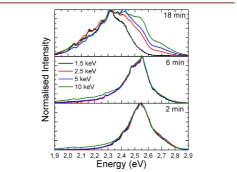
The impact on the luminescent properties of the InGaN shell change in morphology and indium content with growth time was measured by room temperature high resolution
cath-odoluminescence (CL) spectroscopy.44 CL spectra were
acquired at the center of them-plane facet with a 100×150
nm area fast scan.Figure 5displays the CL spectra of the 2, 6,
and 18 min growths for four different accelerating voltages in
the range 1.5−10 kV, in order to probe different depths into the
sample.
For accelerating voltages of 1.5 kV, the electron beam
penetration depth is∼15 nm,45which is sufficient to penetrate
the entire ∼8 nm thickness of the m-plane 2D InGaN layer
grown for 2 min having an emission peak centered at 2.55 eV
(lower pane ofFigure 5). With increasing accelerating voltage,
the peak position and full width at half-maximum remains almost unchanged. Thus, the emission peak centered at 2.55 eV only derives from the initially grown 2D pseudomorphic
InGaN layer. The CL spectra of the ∼22 nm thick 6 min
InGaN growth follow the same trend with increasing the accelerating voltage, with the main emission peak still centered
at 2.55 eV (central pane of Figure 5). However, a small but
perceptible increase in the relative intensity of the low energy tail compared with the main emission peak is observed, which, when comparing with TEM and EDX observations, correlates with a nascent stage of the formation of indium-rich 3D striations in the upper part of the 2D InGaN layer.
Unlike the 2 and 6 min InGaN growth, the CL spectra of the
18 min InGaN growth, displayed in the upper panel ofFigure 5,
show a clear dependence in the CL emission with increasing the accelerating voltage. For 1.5 kV, a broad emission peak centered at 2.32 eV with a higher energy shoulder at 2.42 eV dominates the spectra, whereas no emission peak can be found at 2.55 eV. By gradually increasing the accelerating voltage, the shoulder at 2.42 eV becomes a clearly resolved feature along with the higher energy shoulder corresponding to the 2.55 eV emission peak. Whereas the low 1.5 kV accelerating voltage is
insufficient to excite the 2D InGaN layer, the 10 kV electron
beam penetration depth of ≈50−60 nm is sufficient to excite
[image:6.625.325.567.117.293.2]the full width of the 18 min InGaN layer. Therefore, by correlating depth-resolved CL spectroscopy with AFM, TEM, and EDX observations for the 18 min InGaN growth, the 2.55 eV emission is unambiguously ascribed to the low indium content 2D pseudomorphic InGaN layer, the low energy 2.32 eV emission is related to the high indium content of the 3D relaxed striated InGaN layer, and the middle energy 2.42 eV
emission can be associated with a 2D InGaN partially relaxed wetting layer having an intermediate indium content.
The CL spectroscopy data thus confirm the compositional
differences between the initial 2D layer and the relaxed 3D
striations found by EDX and further reveal a tendency for the volume-averaged indium content of the 3D striated features to increase with growth time.
■
CONCLUSIONIn summary, the underlying growth mechanism of a thick InGaN shell grown on GaN NRs formed by combined top-down etching and regrowth has been described and explained through a correlation between the observed change of the InGaN morphology and composition. Combined AFM, TEM, and EDX evidence shows that the presence of quasi-periodic
atomic steps along thec-axis of them-plane GaN facets of the
NRs induce preferential incorporation of species at or near the
step edges, leading to lateralfluctuations in InN content along
the c-axis. By adopting a step growth mode, the indium
fluctuations build up, and strain inhomogeneity is induced
within the InGaN layer. At a critical thickness, the strain is not gradually and homogeneously relieved through the formation of
misfit dislocations, but instead inhomogeneously relieved
through elastic relaxation and the formation of new facets,
resulting in nanoscale quasi-periodic striations along thec-axis.
The change in morphology subsequently leads to a higher variation in the indium incorporation between the remaining
m-plane and the new inclined facets, with the InGaN 2D layer
acting like a wetting layer. The as-grown thick InGaN consists of several sublayers with distinct compositions and strain states: a thin epitaxially strained 2D layer of low InN mole fraction
having a slight fluctuation in mole fraction; a second, thicker,
partially relaxed 2D layer of higher InN mole fraction and larger
fluctuation; and finally, an upper relaxed section comprising
strongly faceted striations of much higher InN mole fraction
due to a more favorable binding of In atoms on the (1−101)
and (11−24) planes. As such, this work shows that the indium
composition and indium lateralfluctuations of the InGaN layer
can be controlled by tuning the frequency of atomic steps on the NR sidewalls. With a combined top-down etching and regrowth fabrication process, this can be achieved through a
judicious choice of NR etch profile and duration of GaN facet
recovery growth to control the m-plane miscut along the +c
axis. The density of the atomic steps could influence the critical
thickness at which the strain relaxation process takes place, potentially allowing for the growth of thicker smooth InGaN layers without new dislocations forming, and opening the possibility of growing light emitting diodes with emissive layers
wide enough to mitigate efficiency droop. In addition, the
growth of thicker striated InGaN layers having no defects and a broader indium composition range would be valuable for absorption-based devices.
■
EXPERIMENTAL SECTIONTop-Down Fabrication Process. A nickel-based metal mask of 200 nm was created on a GaN on silicon template using a nanoimprint lift-offtechnique, resulting in a hexagonal array of metal dots of∼510 nm diameter with a 2000 nm pitch. Subsequently, the GaN 2D layer was etched into the silicon to achieve a GaN/AlN/Si NR array (Figure S1a). The etching was performed in an inductively coupled plasma (ICP) dry etch system (Oxford Instruments System 100 Cobra) using the following recipe: a Cl2flow of 50 sccm, an Arflow of 10 sccm, 120 W RIE power, 800 W ICP source power, 9 mTorr and 150°C.
Regrowth Process.To promote growth on the NR sidewalls only, the underlying Si was protected from regrowth by passivation achieved by the formation of SiNxon the exposed Si by an in situ MOVPE
nitridation step at 950 °C. MOVPE GaN regrowth faceting was subsequently performed during 6 min at 900°C, 100 mbars with 8 sccm in TMGaflow rate, and 2800 sccm in NH3flow rate (V/III ratio of 3865) to recover the {10−10} nonpolar and {1−101} semipolar facets (Figure S1b). Then, a first set of three different InGaN SQW thickness was grown for 2, 6, and 18 min at 700°C, 300 mbars, 9 sccm in TMGaflow rate, 360 sccm in TMInflow rate (the molar ratio of TMIn in the vapor phase was kept constant at 45% throughout the growths) and 5000 sccm in NH3 flow rate (V/III ratio of 3430) without any GaN cap layer. Finally, the same set of growth was performed for three different times with the same InGaN SQW growth conditions, but this time with a GaN cap layer grown at 850°C, 100 mbars, 9 sccm in TMGaflow rate, and 5000 sccm in NH3flow rate (V/III ratio of 6135).
AFM Characterization and Processing.The as-grown GaN and GaN/InGaN NRs samples were mechanically removed from the Si substrate and dispersed on a host Si substrate. The NRs were then carefully located within a SEM prior to AFM measurements to ensure that the studied NRs were lyingflat on the substrate.
Tapping mode was used for all the AFM measurements. Line flattening on the selected areas of interest was performed to obtain the AFM height image of them-plane facet for the GaN faceted NRs and the three uncapped InGaN samples, as illustrated inFigure S2. The RMS roughness value for each sample was extracted from the center of them-facet to avoid any contribution of the apexes, as illustrated in Figure S2. The images to calculate RMS roughnesses are the same size and have all undergone lineflattening. The height and periodicity of the features or striations were extracted via AFM line scans traced along thec-axis.
TEM and EDX Characterization. The samples for TEM observations and EDX measurements were prepared by a tripod polishing method using an Allied Tech Multiprep unit. Specimens were then ion-milled with a Gatan Precision Ion Polishing System (PIPS) using 1.5−5 keV argon ions for further thinning and removing the residue of polishing contamination from the specimens.
Samples for HRTEM were prepared by a dual beam focused ion beam milling using a FEI Nova 200 NanoLab high resolution field emission gun scanning electron microscope (FEGSEM) with precise focused ion beam (FIB) etch and deposition capabilities. The nanorods were protected by a platinum layer prior to etching to reduce the damage that could occur with the use of an ion beam system.
NRs shown inFigure 4a−d (same inFigure S3a−d) were prepared by a tripod polishing method, whereas the NR shown inFigure 4e was prepared using a focused ion beam.
The low magnification TEM investigations were performed using a FEI Tecnai Osiris fitted with high brightness field emission gun (XFEG). Experiments were carried out at an accelerating voltage of 200 kV and a beam current of 0.5 nA.
The HRTEM observations were performed using a FEI Titan3 Themis 300fitted with high brightness XFEG with S-TWIN objective lens and monochromator (energy spread approximately 0.25 eV).
the k-factor provided by the manufacturer of the EDX system (Bruker). The errors were also estimated from Poisson statistics. The ICA technique is capable of differentiating true spectra from the underlying noise efficiently, and, as a result, noisy spectra can be tolerated. Using the ICA technique, the required sample beam dose was therefore significantly minimized without compromising the accuracy of quantification.
CL Characterization. Cathodoluminescence spectroscopy was carried out at room temperature in a modified FEI Quanta 250field emission SEM with various accelerating voltages. Light was collected using an NA0.28 reflecting objective with its axis perpendicular to the electron beam and focused directly to the entrance of the spectrograph using an off-axis paraboloidal mirror. We used a 125 mm focal length spectrograph with a 600 lines/mm grating and 50μm entrance slit, coupled to a cooled electron multiplying charge-coupled device (EMCCD) detector.
■
ASSOCIATED CONTENT*
S Supporting InformationThe Supporting Information is available free of charge on the ACS Publications websiteat DOI:10.1021/acs.cgd.6b01281.
Additional pictures on GaN/InGaN core−shell NR
fabrication process, AFM acquisitions and processing, TEM pictures and EDX data processing treatment
(PDF)
■
AUTHOR INFORMATIONCorresponding Author
*E-mail: [email protected].
ORCID
Pierre-Marie Coulon: 0000-0002-9120-7554 Duncan W. E. Allsopp: 0000-0003-4197-9852
Present Address
Department of Electronic and Electrical Engineering, Uni-versity of Bath, BA2 7AY, UK
Author Contributions
P.-M.C. and E.D.B. conceived the experimental work, supervised by P.A.S. and D.W.E.A. P.-M.C. carried out the nanorod fabrication, MOVPE growth experiment, and SEM characterization. A.B. and R.A.O performed the AFM character-ization. S.H.V. performed the TEM and EDX characterizations. P.R.E. and R.W.M. performed the CL characterization. All other authors contributed in analyzing and writing the results. Notes
The authors declare no competingfinancial interest.
■
ACKNOWLEDGMENTSThe authors would like to thank OSRAM Opto Semi-conductors GmbH for the provision of the GaN/silicon
templates and acknowledge financial support from the
European Union (FP7 Contract No.: 228999, “SMASH”)
and the EPSRC, UK via Grant No. EP/I012591/1 “Lighting
the Future” and Grant No. EP/M015181/1, “Manufacturing
nano-GaN”. This publication is supported by multiple data sets,
which are openly available here: http://doi.org/10.15125/
BATH-00224.
■
REFERENCES(1) Nakamura, S.; Mukai, T.; Senoh, M.Appl. Phys. Lett.1994,64, 1687.
(2) Nakamura, S.Solid State Commun.1997,102, 237. (3) Mukai, T.; Nakamura, S.Jpn. J. Appl. Phys.1999,38, 5735.
(4) Jani, O.; Ferguson, I.; Honsberg, C.; Kurtz, S.Appl. Phys. Lett.
2007,91, 132117.
(5) Dahal, R.; Pantha, B.; Li, J.; Lin, J. Y.; Jiang, H. X.Appl. Phys. Lett.
2009,94, 063505.
(6) Fujii, K.; Karasawa, T.; Ohkawa, K.Jpn. J. Appl. Phys.2005,44, L543.
(7) Li, J.; Lin, J. Y.; Jiang, H. X.Appl. Phys. Lett.2008,93, 162107. (8) Cho, H. K.; Lee, J. Y.; Yang, G. M.; Kim, C. S.Appl. Phys. Lett.
2001,79, 215.
(9) Cho, H. K.; Lee, J. Y.; Kim, C. S.; Yang, G. M.J. Appl. Phys.2002,
91, 1166.
(10) Thaler, G. T.; Koleske, D. D.; Lee, S. R.; Bogart, K. H. A.; Crawford, M. H.J. Cryst. Growth2010,312, 1817−1822.
(11) El-Masry, N. A.; Piner, E. L.; Liu, S. X.; Bedair, S. M.Appl. Phys. Lett.1998,72, 40.
(12) Chen, Y.; Takeuchi, T.; Amano, H.; Akasaki, I.; Yamada, N.; Kaneko, Y.; Wang, S. Y.Appl. Phys. Lett.1998,72, 710.
(13) Tessarek, C.; Figge, S.; Aschenbrenner, T.; Bley, S.; Rosenauer, A.; Seyfried, M.; Kalden, J.; Sebald, K.; Gutowski, J.; Hommel, D.Phys. Rev. B: Condens. Matter Mater. Phys.2011,83, 115316.
(14) Srinivasan, S.; Geng, L.; Liu, R.; Ponce, F. A.; Narukawa, Y.; Tanaka, S.Appl. Phys. Lett.2003,83, 5187.
(15) Leyer, M.; Stellmach, J.; Meissner, Ch.; Pristovsek, M.; Kneissl, M.J. Cryst. Growth2008,310, 4913−4915.
(16) Pereira, S.; Correia, M. R.; Pereira, E.; O’Donnell, K. P.; Trager-Cowan, C.; Sweeney, F.; Alves, E.Phys. Rev. B2011,60, 205311.
(17) Stringfellow, G. B.J. Cryst. Growth2010,312, 735−749.
(18) Pantzas, K.; Patriarche, G.; Troadec, D.; Gautier, S.; Moudakir, T.; Suresh, S.; Largeau, L.; Mauguin, O.; Voss, P. L.; Ougazzaden, A.
Nanotechnology2012,23, 455707.
(19) Fischer, A. M.; Wu, Z.; Sun, K.; Wei, Q.; Huang, Y.; Senda, R.; Iida, D.; Iwaya, M.; Amano, H.; Ponce, F. A.Appl. Phys. Express2009,
2, 041002.
(20) Neumann, W.; Mogilatenko, A.; Wernicke, T.; Richter, E.; Weyers, M.; Kneissl, M.J. Microsc.2010,237, 308−313.
(21) Hugues, M.; Shields, P. A.; Sacconi, F.; Mexis, M.; Auf der Maur, M.; Cooke, M.; Dineen, M.; Di Carlo, A.; Allsopp, D. W. E.; Zúñ iga-Pérez, J.J. Appl. Phys.2013,114, 084307.
(22) Coulon, P.-M.; Alloing, B.; Brändli, V.; Vennéguès, P.; Leroux, M.; Zúñiga-Perez, J.́ Appl. Phys. Express2016,9, 015502.
(23) Tourbot, G.; Bougerol, C.; Glas, F.; Zagonel, L. F.; Mahfoud, Z.; Meuret, S.; Gilet, P.; Kociak, M.; Gayral, B.; Daudin, B.Nanotechnology
2012,23, 135703.
(24) Woo, S. Y.; Bugnet, M.; Nguyen, H. P. T.; Mi, Z.; Botton, G. A.
Nano Lett.2015,15, 6413−6418.
(25) Li, S.; Waag, A.J. Appl. Phys.2012,111, 071101.
(26) Yanagihara, A.; Ishizawa, S.; Kishino, K. Appl. Phys. Express
2014,7, 112102.
(27) Zhuang, Y. D.; Lewins, C. J.; Lis, S.; Shields, P. A.; Allsopp, D. W. E.IEEE Photonics Technol. Lett.2013,25, 1047−92013.
(28) Wierer, J. J., Jr.; Li, Q.; Koleske, D. D.; Lee, S. R.; Wang, G. T.
Nanotechnology2012,23, 194007.
(29) Koester, R.; Hwang, J.-S.; Salomon, D.; Chen, X.; Bougerol, C.; Barnes, J.-P.; Dang; Dle, S.; Rigutti, L.; de Luna Bugallo, A.; Jacopin, G.; Tchernycheva, M.; Durand, C.; Eymery, J.Nano Lett. 2011,11, 4839−4845.
(30) Yeh, T.-W.; Lin, Y.-T.; Stewart, L. S.; Dapkus, P. D.; Sarkissian, R.; O’Brien, J. D.; Ahn, B.; Nutt, S. R.Nano Lett.2012,12, 3257− 3262.
(31) Liao, C.-H.; Chang, W.-M.; Yao, Y.-F.; Chen, H.-T.; Su, C.-Y.; Chen, C.-Y.; Hsieh, C.; Chen, H.-S.; Tu, C.-G.; Kiang, Y.-W.; Yang, C. C.; Hsu, T.-C.J. Appl. Phys.2013,113, 054315.
(32) Ra, Y. H.; Navamathavan, R.; Park, J. H.; Lee, C. R.Nano Lett.
2013,13, 3506−3516.
(33) Le Boulbar, E. D.; Edwards, P. R.; Vajargah, S. H.; Griffiths, I.; Gîrgel, I.; Coulon, P.-M.; Cherns, D.; Martin, R. W.; Humphreys, C. J.; Bowen, C. R.; Allsopp, D. W. E.; Shields, P. A.Cryst. Growth Des.
(34) Shields, P. A.; Allsopp, D. W. E.Microelectron. Eng.2011,88, 3011.
(35) Le Boulbar, E. D.; Gîrgel, I.; Lewins, C. J.; Edwards, P. R.; Martin, R. W.; Šatka, A.; Allsopp, D. W. E.; Shields, P. A.J. Appl. Phys.
2013,114, 094302.
(36) Lewins, C. J.; Le Boulbar, E. D.; Lis, S. M.; Edwards, P. R.; Martin, R. W.; Shields, P. A.; Allsopp, D. W. E.J. Appl. Phys.2014,116, 044305.
(37) Lu, P. F.; Sun, C.; Cao, H. W.; Ye, H.; Zhong, X. X.; Yu, Z. Y.; Han, L. H.; Wang, S. M.Solid State Commun.2014,178, 1−6.
(38) Northrup, J. E.; Romano, L. T.; Neugebauer, J.Appl. Phys. Lett.
1999,74, 2319.
(39) Kelchner, K. M.; Kuritzky, L. Y.; Nakamura, S.; DenBaars, S. P.; Speck, J. S.J. Cryst. Growth2015,411, 56−62.
(40) Kaufmann, N. A. K.; Lahourcade, L.; Hourahine, B.; Martin, D.; Grandjean, N.J. Cryst. Growth2016,433, 36−42.
(41) Shiojiri, M.; Chuo, C. C.; Hsu, J. T.; Yang, J. R.; Saijo, H.J. Appl. Phys.2006,99, 073505.
(42) Richard, M.-I.; Highland, M. J.; Fister, T. T.; Munkholm, A.; Mei, J.; Streiffer, S. K.; Thompson, C.; Fuoss, P. H.; Stephenson, G. B.
Appl. Phys. Lett.2010,96, 051911.
(43) Stankevic, T.; Mickevicius, S.; Nielsen, M. S.; Kryliouk, O.; Ciechonski, R.; Vescovi, G.; Bi, Z.; Mikkelsen, A.; Samuelson, L.; Gundlach, C.; Feidenhans’l, R.J. Appl. Crystallogr.2015,48, 344−349.
(44) Edwards, P. R.; Jagadamma, L. K.; Bruckbauer, J.; Liu, C.; Shields, P.; Allsopp, D.; Wang, T.; Martin, R. W.Microsc. Microanal.
2012,18, 1212−1219.