coatings
Article
Automated Control of Plasma Ion-Assisted Electron
Beam-Deposited TiO
2
Optical Thin Films
Bing Hui1,2, Xiuhua Fu1,*, Des Gibson2,*ID, David Child2, Shigeng Song2ID, Lewis Fleming2, Guntis Rutins2, Hin on Chu2, Caspar Clark3and Stuart Reid4
1 School of OptoElectronic Engineering, Changchun University of Science and Technology,
Changchun 130012, China; huibing1994@outlook.com
2 Scottish Universities Physics Alliance (SUPA), The Institute for Thin Films, Sensors & Imaging,
University of the West of Scotland, Paisley PA1 2BE, UK; david.child@uws.ac.uk (D.C.); shigeng.song@uws.ac.uk (S.S.); lewis.fleming@uws.ac.uk (L.F.); guntis.rutins@uws.ac.uk (G.R.); hinon.chu@uws.ac.uk (H.o.C.)
3 CJS Instrumentation Ltd., Easter Inch Industrial Estate, Bathgate EH48 2FJ, UK; caspar@cjsi.co.uk 4 Scottish Universities Physics Alliance (SUPA), Department of Biomedical Engineering,
University of Strathclyde, Glasgow G1 1QE, UK; stuart.reid@strath.ac.uk * Correspondence: fuxiuhua@cust.edu.cn (X.F.); des.gibson@uws.ac.uk (D.G.);
Tel.: +86-1360-443-5770 (X.F.); +44-141-848-3610 (D.G.)
Received: 4 July 2018; Accepted: 3 August 2018; Published: 5 August 2018
Abstract: A hollow cathode plasma source has been operated automatically, demonstrating independent control of plasma ion energy and ion current density for plasma ion-assisted electron beam-deposited titania (TiO2). The lanthanum hexaboride hollow cathode design described in this
work utilizes both the interior and exterior cathode surfaces, with the additional electrons generated removing the need for a separate neutralizing source. Automatic feedback control of plasma source cathode-to-anode accelerator voltage (AV—via argon gas flow to the anode and/or cathode plasma source areas) and accelerator current (AC—via an external high-current power supply) provides independent control of the ion energy distribution function and ion current density, respectively. Automated run-to-run reproducibility (over six separate deposition runs) in TiO2refractive index
(550 nm) was demonstrated as 2.416±0.008 (spread quoted as one standard deviation), which is well within the required refractive index control for optical coating applications. Variation in refractive index is achievable through control of AV (ion energy) and/or AC (ion current density), directly influencing deposited TiO2structural phase. Measured dependencies of TiO2refractive index and
extinction coefficient on AV and AC are described. Optimum plasma source parameters for assisted electron beam deposition of TiO2optical thin-film applications are highlighted.
Keywords:plasma ion source; Titania; refractive index; accelerator current; accelerator voltage
1. Introduction
In plasma ion beam-assisted deposition, the arrival of low-energy evaporation from electron beam evaporators is complemented by high-energy plasma ions, typically in the ion energy range from 1 to 100 eV at ion current densities between 1 and 1000µA/cm2[1]. A significant amount of work concerning phase formation, heteroepitaxy, stress engineering and adhesion properties has been published and reviewed in the literature [1–3]. At the same time, technological applications including optical thin-film deposition have been reported [4–6]. Advantageous is the independent variation of process parameters for ion beam and low-energy evaporation flux, as the ion energy and ion current density can be varied independently from the evaporation flux density [7]. The technological
acceptance and utilization are closely connected with the development of modern broad-beam ion [8] and plasma sources [9], leading to recent developments of commercial ion or plasma beam systems for large-area and flat substrates by different companies [10]. All of these metrics emphasize the interdependence on the film temperature, ion current density and the ion energy. It is convenient when quantifying and comparing the effects of plasma ion-assisted depositions to focus on a well-categorized optical material. As such, this work concentrates on titania (TiO2), which has been extensively
studied owing to its wide range of applications [11–13]. Plasma ion-assisted deposition of optical thin films must allow precise control and reproducibility of the complex refractive index while maintaining the wavelength dependence (dispersion) of the refractive index,n(λ), and of the extinction coefficient,k(λ). These are governed by fundamental dispersion relations that depend on the material’s microstructure [14]. In practical applications, thenvalues should be precisely controlled to typically 1 part in 100 for optical thin films with extinction coefficient minimized [15]. This work describes automated control of a plasma source [4,16] for independent control of ion energy and ion current density for ion-assisted electron beam deposition of a commonly used high-refractive-index material, TiO2. Plasma ion-assisted electron beam deposition of TiO2to achieve reproducible TiO2film optical
properties is particularly challenging, primarily due to both a rapidly changing n(λ) dispersion characteristic and also different structural phases (primarily anatase and rutile) with differingn(λ) characteristics [14]. Amorphous/anatase are the preferred structural phases for optical thin films as the material is isotropic with low extinction coefficient [14]. The primary aim of this work is to demonstrate required automated and reproducible run-to-run control of TiO2 film n(λ) and k(λ), suitable for
reproducible deposition of optical thin films. The novelty reported in this work is independent automatic control of ion energy and ion current density for precision control of plasma ion-assisted electron beam deposition of TiO2[4].
2. Plasma Source and Electron Beam Deposition System Description
This work utilizes a novel plasma source [16] based on a newly proposed configuration [16]. Schematic and cross-sectional views of the plasma source are shown in Figure1. The induction coil shown in Figure1operates at a radio frequency of typically 100 kHz (Ambrell EKOHEAT induction supply, Rochester, NY, USA), inductively heating inner and outer surfaces of a lanthanum hexaboride (high-efficiency thermionic emitter [17]) hollow cathode. The water-cooled induction coil provides an optimum skin depth for heating of the hollow cathode’s inner and outer surfaces [4,16].
Coatings 2018, 8, x FOR PEER REVIEW 2 of 11
broad-beam ion [8] and plasma sources [9], leading to recent developments of commercial ion or plasma beam systems for large-area and flat substrates by different companies [10]. All of these metrics emphasize the interdependence on the film temperature, ion current density and the ion energy. It is convenient when quantifying and comparing the effects of plasma ion-assisted depositions to focus on a well-categorized optical material. As such,this work concentrates on titania (TiO2), which has been extensively studied owing to its wide range of applications [11–13].Plasma
ion-assisted deposition of optical thin films must allow precise control and reproducibility of the complex refractive index while maintaining the wavelength dependence (dispersion) of the refractive index, n(λ), and of the extinction coefficient, k(λ). These are governed by fundamental dispersion relations that depend on the material’s microstructure [14]. In practical applications, the n values should be precisely controlled to typically 1 part in 100 for optical thin films with extinction coefficient minimized [15]. This work describes automated control of a plasma source [4,16] for independent control of ion energy and ion current density for ion-assisted electron beam deposition of a commonly used high-refractive-index material, TiO2. Plasma ion-assisted electron beam
deposition of TiO2 to achieve reproducible TiO2 film optical properties is particularly challenging,
primarily due to both a rapidly changing n(λ) dispersion characteristic and also different structural phases (primarily anatase and rutile) with differing n(λ) characteristics [14]. Amorphous/anatase are the preferred structural phases for optical thin films as the material is isotropic with low extinction coefficient [14]. The primary aim of this work is to demonstrate required automated and reproducible run-to-run control of TiO2 film n(λ) and k(λ), suitable for reproducible deposition of optical thin films.
The novelty reported in this work is independent automatic control of ion energy and ion current density for precision control of plasma ion-assisted electron beam deposition of TiO2 [4].
2. Plasma Source and Electron Beam Deposition System Description
This work utilizes a novel plasma source [16] based on a newly proposed configuration [16]. Schematic and cross-sectional views of the plasma source are shown in Figure 1. The induction coil shown in Figure 1 operates at a radio frequency of typically 100 kHz (Ambrell EKOHEAT induction supply, Rochester, NY, USA), inductively heating inner and outer surfaces of a lanthanum hexaboride (high-efficiency thermionic emitter [17]) hollow cathode. The water-cooled induction coil provides an optimum skin depth for heating of the hollow cathode’s inner and outer surfaces [4,16].
[image:2.595.158.437.524.704.2](a) (b)
Figure 1. Plasma source schematic (a) and cross-section photo (b) (plasma source dimensions: height 200 mm; width 150 mm). Hollow cathode material is lanthanum hexaboride and restrictor plate material boron nitride. Main body (anode) material is water-cooled stainless steel.
The generated thermionic electrons from the inductively heated lanthanum hexaboride hollow cathode are subsequently given sufficient energy through an accelerating voltage (AV) between the cathode and anode. This results in ionization of heavier gas atoms such as argon, separately
Coatings2018,8, 272 3 of 11
The generated thermionic electrons from the inductively heated lanthanum hexaboride hollow cathode are subsequently given sufficient energy through an accelerating voltage (AV) between the cathode and anode. This results in ionization of heavier gas atoms such as argon, separately introduced into the plasma source cathode and anode regions. Other plasma source features include axially displaced anode and cathode electrodes with decoupled magnetic fields in the anode and cathode regions, enabling separate control of the plasma ion energy, ion current density and spatial distribution within the chamber [4,16]. The plasma ion energy is controlled through variation in the cathode-to-anode voltage (AV)—achieved via variation in argon gas flow into the anode and/or cathode regions with resulting change in cathode-to-anode impedance and hence voltage. Process gas (oxygen for thin-film oxide deposition) is introduced at the plasma source output as shown in Figure1. Ion current density is varied by controlling cathode-to-anode accelerator current (AC) from an external power supply (power supply type Advanced Energy Pinnacle 10 kW DC). The resulting plasma is magnetically confined within the anode region using an energized solenoid coil (power supply type ETPS LAB DSP 030-025, Chesterfield, UK) shown in Figure1[4,16]. Variation in solenoid coil current also provides a means of tuning ion current density spatial distribution external to the plasma source across the deposition area [16]. The plasma ion beam’s spatial profile can be tuned using the extractor coil depending on size of the deposition area (small area, high solenoid current (>10 A) to confine plasma extent, and large area, low solenoid current (<10 A) to allow plasma to spread). Plasma ion current density measurements across the Satis 370 calotte area using a Faraday cup [4] indicate plasma ion current density of 0.4 mA/cm2(for plasma source running conditions AV = 145 V; AC = 35 A) with <5% variation within the measurement accuracy (Satis 370 0.8 m calotte diameter with extractor current = 12 A). Use of a boron nitride restrictor plate (with a centralized aperture typically 10-mm diameter) between the cathode and anode, as shown in Figure1, increases operating pressure in the cathode region by typically 10×compared to the main chamber pressure (10−3mbar cf. 10−4mbar) [4] and resulting ionization efficiency. Use of a boron nitride restrictor plate has two advantages, listed as follows:
• Reduces heating loading from the cathode region to the chamber deposition area by typically 60%, and reduces defect incorporation into the deposited film [4]).
• Self-sustained plasma is possible without cathode inductive heating—plasma density is sufficient to heat the hollow cathode without use of induction coil power (for self-sustained operation, cathode-to-anode current is typically >15 A) [4,16].
Coatings 2018, 8, x FOR PEER REVIEW 3 of 11
introduced into the plasma source cathode and anode regions. Other plasma source features include axially displaced anode and cathode electrodes with decoupled magnetic fields in the anode and cathode regions, enabling separate control of the plasma ion energy, ion current density and spatial distribution within the chamber [4,16]. The plasma ion energy is controlled through variation in the cathode-to-anode voltage (AV)—achieved via variation in argon gas flow into the anode and/or cathode regions with resulting change in cathode-to-anode impedance and hence voltage. Process gas (oxygen for thin-film oxide deposition) is introduced at the plasma source output as shown in Figure 1. Ion current density is varied by controlling cathode-to-anode accelerator current (AC) from an external power supply (power supply type Advanced Energy Pinnacle 10 kW DC). The resulting plasma is magnetically confined within the anode region using an energized solenoid coil (power supply type ETPS LAB DSP 030-025, Chesterfield, UK) shown in Figure 1 [4,16]. Variation in solenoid coil current also provides a means of tuning ion current density spatial distribution external to the plasma source across the deposition area [16]. The plasma ion beam’s spatial profile can be tuned using the extractor coil depending on size of the deposition area (small area, high solenoid current (>10 A) to confine plasma extent, and large area, low solenoid current (<10 A) to allow plasma to spread). Plasma ion current density measurements across the Satis 370 calotte area using a Faraday cup [4] indicate plasma ion current density of 0.4 mA/cm2 (for plasma source running conditions AV
= 145 V; AC = 35 A) with <5% variation within the measurement accuracy (Satis 370 0.8 m calotte diameter with extractor current = 12 A). Use of a boron nitride restrictor plate (with a centralized aperture typically 10-mm diameter) between the cathode and anode, as shown in Figure 1, increases operating pressure in the cathode region by typically 10× compared to the main chamber pressure (10−3 mbar cf. 10−4 mbar) [4] and resulting ionization efficiency. Use of a boron nitride restrictor plate
has two advantages, listed as follows:
Reduces heating loading from the cathode region to the chamber deposition area by typically 60%, and reduces defect incorporation into the deposited film [4]).
Self-sustained plasma is possible without cathode inductive heating—plasma density is sufficient to heat the hollow cathode without use of induction coil power (for self-sustained operation, cathode-to-anode current is typically >15 A) [4,16].
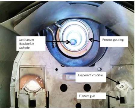
[image:3.595.187.411.528.709.2]Plasma-assisted electron beam deposition work reported in this paper was carried out using a Satis 370 box coater (Satis MC370 chamber, Milan, Italy). The system has two electron guns (electron beam turret source model Temescal STIH-270-2PT, Santa Clara, CA, USA) and is turbo pumped (Pfeiffer TPH 2101P, Asslar, Germany) with a dry backing pump (Ebara A10S, Chelmsford, MA, USA). A cryocooler (Poly-cold PFC 550-ST, Tokyo, Japan) is used for water pumping. Achieved base vacuum is typically 1 × 10⁻⁷ mbar. Baseplate configuration is shown in Figure 2, indicating two electron beam deposition guns (one utilized for this work) and the plasma source located equidistant from each deposition source.
Figure 2.Figure 2. Satis 370 electron beam deposition system baseplate configuration. Satis 370 electron beam deposition system baseplate configuration.
beam turret source model Temescal STIH-270-2PT, Santa Clara, CA, USA) and is turbo pumped (Pfeiffer TPH 2101P, Asslar, Germany) with a dry backing pump (Ebara A10S, Chelmsford, MA, USA). A cryocooler (Poly-cold PFC 550-ST, Tokyo, Japan) is used for water pumping. Achieved base vacuum is typically 1×10⁻⁷mbar. Baseplate configuration is shown in Figure2, indicating two electron beam deposition guns (one utilized for this work) and the plasma source located equidistant from each deposition source.
3. Influence of Plasma Ion Energetics in Film Growth and Control
A simple unifying parameter often used in plasma ion energetics is represented by the energy per deposited evaporation particle of the film (Ep), first proposed by Harper et al. in 1984 [18]. Specific relationship is shown as follows:
(EP) =Ei(Φi/Φn) (1)
whereEiis the ion energy controlled by cathode-to-anode voltage (acceleration voltage—AV), andΦi is the ion current density controlled by cathode-to-anode current (accelerating current—AC).Φiand Φn in Equation (1) are the ion and condensing particle fluxes, respectively, with plasma source operating parameters ion current density (cathode-to-anode accelerating current (AC)) and ion energy (cathode-to-anode accelerating voltage (AV)) [4]. It is a particular need for control of the deposition process by selective adjustment of the ion energy (Ei) and ion flux (Φi) that has driven the development of such ion- and plasma-assisted processes [15]. The key parameters that control the film microstructure in low-pressure deposition processes areEiandΦi, adjusted with a separate plasma ion source. In the pressure range (low 10−4mbar) generally used for electron beam deposition, the plasma ions lose part of their energy due to elastic, inelastic, and charge-transfer collisions in the sheath, exhibiting a relatively broad plasma ion energy distribution function (IEDF). Measured typical IEDF for this work (Faraday cup measurement 0.5 m above the plasma source at the substrate plane [4]) is shown in Figure3.
Coatings 2018, 8, x FOR PEER REVIEW 4 of 11
3. Influence of Plasma Ion Energetics in Film Growth and Control
A simple unifying parameter often used in plasma ion energetics is represented by the energy per deposited evaporation particle of the film (𝐸𝑝), first proposed by Harper et al. in 1984 [18]. Specific
relationship is shown as follows:
(𝐸𝑃) = 𝐸𝑖(Φ𝑖⁄Φ𝑛) (1)
where 𝐸𝑖 is the ion energy controlled by cathode-to-anode voltage (acceleration voltage—AV), and
Φ𝑖 is the ion current density controlled by cathode-to-anode current (accelerating current—AC). Φ𝑖
and Φ𝑛 in Equation (1) are the ion and condensing particle fluxes, respectively, with plasma source
operating parameters ion current density (cathode-to-anode accelerating current (AC)) and ion energy (cathode-to-anode accelerating voltage (AV)) [4]. It is a particular need for control of the deposition process by selective adjustment of the ion energy (𝐸𝑖) and ion flux (Φ𝑖) that has driven the
development of such ion- and plasma-assisted processes [15]. The key parameters that control the film microstructure in low-pressure deposition processes are 𝐸𝑖 and Φ𝑖, adjusted with a separate
plasma ion source. In the pressure range (low 10−4 mbar) generally used for electron beam deposition,
[image:4.595.191.409.451.604.2]the plasma ions lose part of their energy due to elastic, inelastic, and charge-transfer collisions in the sheath, exhibiting a relatively broad plasma ion energy distribution function (IEDF). Measured typical IEDF for this work (Faraday cup measurement 0.5 m above the plasma source at the substrate plane [4]) is shown in Figure 3.
Figure 3. Plasma source measured Ion Energy Distribution Function (IEDF) function.
The ion distribution in Figure 3 is typical of hollow cathodes, and much research has been carried out, typified by Goebel et al. [19,20]. Typically, a peak is observed at about the discharge voltage (term 2 in Figure 3) with a corresponding, larger peak at typically around 50% of the discharge voltage (term 1 in Figure 3), similar to the ion energy distribution measured in Figure 3. This lower peak is described by Goebel [17] as representing the potential at which the ions were created, inferring that in this case the majority of the ions impinging on the Faraday cup (at the substrate surface position) are created by secondary collisions in the plasma plume rather than within the hollow cathode or anode area [19]. Previous work [4,15] suggests that good-quality (dense, hard, chemically stable, low stress) films are preferably deposited under conditions of low (10–50 eV) ion energies, sufficient for densification, however using high Φ𝑖. This reduces the microstructural
damage and gas entrapment, generally yielding low-film-stress values whilst achieving high refractive index and spectral stability. High ion fluxes are very advantageous, especially when aiming to achieve amorphous low-roughness coatings with low optical absorption [4,15]. 𝐸𝑖 and Φ𝑖 in
Equation (1) can be separately controlled within the plasma source via control of cathode-to-anode accelerating voltage (AV) and current (AC), respectively. The plasma source operational block diagram with associated control loops is shown in the Figure 4. The plasma source was controlled by a computer/programmable logic controller (PC/PLC) which can automatically adjust gas, RF induction power, argon and oxygen gas flow, and DC and extractor coil currents. The PLC was
Figure 3.Plasma source measured Ion Energy Distribution Function (IEDF) function.
Coatings2018,8, 272 5 of 11
densification, however using highΦi. This reduces the microstructural damage and gas entrapment, generally yielding low-film-stress values whilst achieving high refractive index and spectral stability. High ion fluxes are very advantageous, especially when aiming to achieve amorphous low-roughness coatings with low optical absorption [4,15]. EiandΦi in Equation (1) can be separately controlled within the plasma source via control of cathode-to-anode accelerating voltage (AV) and current (AC), respectively. The plasma source operational block diagram with associated control loops is shown in the Figure4. The plasma source was controlled by a computer/programmable logic controller (PC/PLC) which can automatically adjust gas, RF induction power, argon and oxygen gas flow, and DC and extractor coil currents. The PLC was sourced from Amplicon and the PC used a Visual Basic C++ front end. Note cathode-to-anode voltage is controlled by anode and/or cathode Ar gas flows, indicated as anode Ar (mass flow controller (MFC 2)) and cathode Ar (MFC 3) gas flows. Process gas (oxygen used in this work) flow is controlled by MFC 1.
Coatings 2018, 8, x FOR PEER REVIEW 5 of 11
[image:5.595.122.474.263.458.2]sourced from Amplicon and the PC used a Visual Basic C++ front end. Note cathode-to-anode voltage is controlled by anode and/or cathode Ar gas flows, indicated as anode Ar (mass flow controller (MFC 2)) and cathode Ar (MFC 3) gas flows. Process gas (oxygen used in this work) flow is controlled by MFC 1.
Figure 4. Plasma source operation and control loops block diagram—personal computer/programmable logic controller (PC/PLC), mass flow controller (MFC)
MFCs 2 and/or 3 are automatically adjusted to maintain constant cathode-to-anode voltage— and thereby 𝐸𝑖. Typical required Ar gas flow changes to maintain constant 𝐸𝑖are <5 Standard Cubic
Centimeters per Minute (sccms), resulting in negligible chamber pressure change.
4. Experimental Conditions and Method
The experimental conditions used in this work are summarized in Table 1.
Table 1. The conditions of experiment and its parameters.
Experimental and Conditions Parameter
Vacuum during deposition 1.0 × 10⁻⁴ mbar
Deposition rate 1.5 Å/s
Temperature Room temperature
Film thickness 500 nm
RF induction power 3.0 kW, 102 kHz
Accelerator current—AC 10, 15, 20, 25, 30, 35 A Accelerator voltage—AV 100, 115, 130, 145, 160, 175, 190 V
The experimental method involved plasma ion-assisted electron beam deposition of TiO2 thin
films onto borosilicate and silicon substrates at room temperature, carried out in a Satis 370 box coater system described in Section 3. This system has a single-axis rotating calotte sample holder with adjustable speed, providing enhanced film physical thickness uniformity. Substrates were cleaned ultrasonically with anhydrous ethanol, acetone and deionized water for 20 min and then dry loaded onto the calotte substrate holder within the deposition chamber. Substrate sizes are 25-mm diameter and 1-mm thick borosilicate material (JGS1) and also 3”-diameter silicon wafers. Evaporation material was Ti3O5 (purity >99.9%) contained within a graphite crucible. The vacuum chamber was
[image:5.595.158.439.628.728.2]pumped down to a typical base pressure of 1.0 × 10⁻⁶ mbar. Prior to deposition, the plasma source was used for substrate cleaning with a 10 min exposure to an argon plasma (AV = 145 V, AC = 25 A). The cathode and anode Ar gas were both argon (research grade 99.999%), and the process gas was oxygen (research grade 99.99%). Pressure was maintained at 1.0 × 10⁻⁴ mbar during deposition.
Figure 4.Plasma source operation and control loops block diagram—personal computer/programmable logic controller (PC/PLC), mass flow controller (MFC).
MFCs 2 and/or 3 are automatically adjusted to maintain constant cathode-to-anode voltage—and therebyEi. Typical required Ar gas flow changes to maintain constantEi are <5 Standard Cubic Centimeters per Minute (sccms), resulting in negligible chamber pressure change.
4. Experimental Conditions and Method
The experimental conditions used in this work are summarized in Table1.
Table 1.The conditions of experiment and its parameters.
Experimental and Conditions Parameter
Vacuum during deposition 1.0×10⁻⁴mbar
Deposition rate 1.5 ˚A/s
Temperature Room temperature
Film thickness 500 nm
RF induction power 3.0 kW, 102 kHz Accelerator current—AC 10, 15, 20, 25, 30, 35 A Accelerator voltage—AV 100, 115, 130, 145, 160, 175, 190 V
The experimental method involved plasma ion-assisted electron beam deposition of TiO2thin
system described in Section3. This system has a single-axis rotating calotte sample holder with adjustable speed, providing enhanced film physical thickness uniformity. Substrates were cleaned ultrasonically with anhydrous ethanol, acetone and deionized water for 20 min and then dry loaded onto the calotte substrate holder within the deposition chamber. Substrate sizes are 25-mm diameter and 1-mm thick borosilicate material (JGS1) and also 3”-diameter silicon wafers. Evaporation material was Ti3O5(purity > 99.9%) contained within a graphite crucible. The vacuum chamber was pumped
down to a typical base pressure of 1.0×10⁻⁶mbar. Prior to deposition, the plasma source was used for substrate cleaning with a 10 min exposure to an argon plasma (AV = 145 V, AC = 25 A). The cathode and anode Ar gas were both argon (research grade 99.999%), and the process gas was oxygen (research grade 99.99%). Pressure was maintained at 1.0×10⁻⁴mbar during deposition. Plasma source currents
(AC: 10 A, 15 A, 20 A, 25 A, 30 A and 35 A) and voltages (AV: 100 V, 115 V, 130 V, 145 V, 160 V, 175 V and 190 V) were used during plasma ion-assisted deposition over a range of deposition runs. The other deposition parameters were constant (indicated in Table1): plasma source RF induction power 3.0 kW with a running frequency of 100 kHz, deposition rate 1.5 ˚A/s and the final single-film physical thickness set at 500 nm. The deposition rate was monitored and controlled with a 6-MHz quartz crystal microbalance and a Kurt J Lesker FTC-2800 deposition controller (Jefferson Hills, PA, USA). A Perkin Elmer (Waltham, MA, USA) Lambda 40 UV/visible spectrometer was used to measure the TiO2optical film spectral transmission. Siemens D5000 X-ray diffractometer (Munich, Germany) was
used to obtain x-ray diffraction patterns of deposited TiO2films.
5. Results and Analysis
5.1. TiO2Structure Characterization
X-ray diffraction (XRD) provides a means of investigating the structure of TiO2. Mergel [21]
mentioned that for electron beam-deposited TiO2, amorphous structure was always found for substrate
temperatures below 300◦C (with no plasma ion assist). Oliver [22] has also indicated that the TiO2
coating obtained by electron gun deposition with no plasma ion-assisted deposition typically exhibits a porous structure. However, TiO2 coating with crystal structure is produced by electron beam
deposition with plasma ion-assisted deposition. TiO2has three distinct crystalline phases: brookite,
rutile and anatase phases [23], however, only the rutile and anatase structure can be observed. Figure5
shows results of XRD and the range of XRD is 2θ(from 20◦to 60◦).
Coatings 2018, 8, x FOR PEER REVIEW 6 of 11
Plasma source currents (AC: 10 A, 15 A, 20 A, 25 A, 30 A and 35 A) and voltages (AV: 100 V, 115 V, 130 V, 145 V, 160 V, 175 V and 190 V) were used during plasma ion-assisted deposition over a range of deposition runs. The other deposition parameters were constant (indicated in Table 1): plasma source RF induction power 3.0 kW with a running frequency of 100 kHz, deposition rate 1.5 Å/s and the final single-film physical thickness set at 500 nm. The deposition rate was monitored and controlled with a 6-MHz quartz crystal microbalance and a Kurt J Lesker FTC-2800 deposition controller (Jefferson Hills, PA, USA). A Perkin Elmer (Waltham, MA, USA) Lambda 40 UV/visible spectrometer was used to measure the TiO2 optical film spectral transmission. Siemens D5000 X-ray
diffractometer (Munich, Germany) was used to obtain x-ray diffraction patterns of deposited TiO2
films.
5. Results and Analysis
5.1. TiO2 Structure Characterization
X-ray diffraction (XRD) provides a means of investigating the structure of TiO2. Mergel [21]
mentioned that for electron beam-deposited TiO2, amorphous structure was always found for
substrate temperatures below 300 °C (with no plasma ion assist). Oliver [22] has also indicated that the TiO2 coating obtained by electron gun deposition with no plasma ion-assisted deposition typically
exhibits a porous structure. However, TiO2 coating with crystal structure is produced by electron
beam deposition with plasma ion-assisted deposition. TiO2 has three distinct crystalline phases:
[image:6.595.217.379.516.714.2]brookite, rutile and anatase phases [23], however, only the rutile and anatase structure can be observed . Figure 5 shows results of XRD and the range of XRD is 2θ (from 20° to 60°).
Figure 5. XRD results for a range of AV/AC settings, for current settings below 35 A it was found that amorphous TiO2 phases are observed in the XRD pattern. Peaks for anatase phases (101) and (112) were observed when AC was set to 35 A.
From Figure 5, the structure of TiO2 optical thin films is shown with constant AV and increasing
AC. Figure 5 indicates with less than (or equal to) 20 A and 145 V, no crystalline structure is observed, suggesting an amorphous structure. With increasing plasma power (increasing AC), evidence of TiO2
crystalline structure is observed (amorphous with anatase structure)—145 V/35 A and above shows several peaks, corresponding to anatase phases of (101) with peak intensity increased with increasing plasma AC. Under the condition of 145 V, 35 A, the TiO2 coatings are a mixture of crystalline (anatase)
and amorphous. With increasing plasma power, the proportion of anatase phase increases as evidenced by an increasing XRD peak at 101. Anatase TiO2 phase, the preferred phase for optical
Coatings2018,8, 272 7 of 11
From Figure5, the structure of TiO2optical thin films is shown with constant AV and increasing
AC. Figure5indicates with less than (or equal to) 20 A and 145 V, no crystalline structure is observed, suggesting an amorphous structure. With increasing plasma power (increasing AC), evidence of TiO2
crystalline structure is observed (amorphous with anatase structure)—145 V/35 A and above shows several peaks, corresponding to anatase phases of (101) with peak intensity increased with increasing plasma AC. Under the condition of 145 V, 35 A, the TiO2coatings are a mixture of crystalline (anatase)
and amorphous. With increasing plasma power, the proportion of anatase phase increases as evidenced by an increasing XRD peak at 101. Anatase TiO2phase, the preferred phase for optical applications, is
present with amorphous TiO2at 145 V, 35 A and above. Table2provides information, by using the
[image:7.595.77.521.259.324.2]Scherrer equation where the shape factor is set to 0.9, regarding the crystallite size trends.
Table 2.XRD analysis providing crystallite size trend data based from the Scherrer equation.
Accelerator Voltage (V) Current (A) (101) Crystallite Size (nm) (112) Crystallite Size (nm)
175 35 19.48 25.27
160 35 9.60 19.05
145 35 8.96 15.04
145 20 NA NA
These XRD patterns show no significant evidence for rutile phases, as their specific peaks are not observed. This implies that the plasma-enhanced electron beam-evaporated TiO2has preferential
growth for amorphous and anatase phases.
5.2. Optical Characterization
The spectral transmittance for TiO2 optical thin films deposited at room temperature and
300◦C substrate temperatures (with no plasma ion assist) are shown in Figure6a and compared with plasma ion-assisted deposited films (current = 35 A, voltage = 145 V) at room temperature. Minimum-to-maximum transmission difference is an indicator of refractive index (increased minimum-to-maximum transmission indicates increasing refractive index).n(λ) andk(λ) dispersion characteristics are derived from the measured spectral transmittance characteristics using the Stephen K. O’Leary, S. R. Johnson, and P. K. Lim (OJL) model [24] and the Kramers–Kronig relationship [25,26]. Figure6b showsn(λ) dispersive characteristics for the three deposition scenarios indicated in Figure6a.
Coatings 2018, 8, x FOR PEER REVIEW 7 of 11
applications, is present with amorphous TiO2 at 145 V, 35 A and above. Table 2 provides information,
by using the Scherrer equation where the shape factor is set to 0.9, regarding the crystallite size trends.
Table 2. XRD analysis providing crystallite size trend data based from the Scherrer equation.
Accelerator Voltage (V) Current (A) (101) Crystallite Size (nm) (112) Crystallite Size (nm)
175 35 19.48 25.27
160 35 9.60 19.05
145 35 8.96 15.04
145 20 NA NA
These XRD patterns show no significant evidence for rutile phases, as their specific peaks are not observed. This implies that the plasma-enhanced electron beam-evaporated TiO2 has preferential
growth for amorphous and anatase phases.
5.2. Optical Characterization
The spectral transmittance for TiO2 optical thin films deposited at room temperature and 300 °C
substrate temperatures (with no plasma ion assist) are shown in Figure 6a and compared with plasma ion-assisted deposited films (current = 35 A, voltage = 145 V) at room temperature. Minimum-to-maximum transmission difference is an indicator of refractive index (increased minimum-to-maximum transmission indicates increasing refractive index). n(λ) and k(λ) dispersion characteristics are derived from the measured spectral transmittance characteristics using the Stephen K. O’Leary, S. R. Johnson, and P. K. Lim (OJL) model [24] and the Kramers–Kronig relationship [25,26]. Figure 6b shows n(λ) dispersive characteristics for the three deposition scenarios indicated in Figure 6a.
(a) (b)
Figure 6. (a) Spectral transmittance of TiO2 optical thin films deposited at room temperature and 300 °C substrate temperatures (no plasma ion-assisted deposition) and plasma ion-assisted deposition (current = 35 A, voltage = 145 V) at room temperature. (b) Shows n(λ) dispersive characteristics for the three deposition scenarios shown in (a).
Figure 7a,b shows n(550 nm) and k(550 nm) as a function of both AC and AV, indicating three distinct regions relating to TiO2 amorphous, anatase and rutile phase content.
Figure7a,b showsn(550 nm) andk(550 nm) as a function of both AC and AV, indicating three distinct regions relating to TiO2amorphous, anatase and rutile phase content.
Coatings 2018, 8, x FOR PEER REVIEW 8 of 11
[image:8.595.98.500.131.287.2](a) (b)
Figure 7. (a) n(550 nm) dispersion characteristics and (b) k(550 nm) dispersion characteristics. The AV represents the different accelerator voltage with constant current (15 A). The AC reflects the different accelerator current with the same voltage (145 V).
Figure 7 indicates increasing refractive index with both increasing AV (ion energy) and AC (ion current density). Both increasing AV and AC result in increased refractive index as a consequence of increased film packing density. Increased AV, providing higher ion energy, and AC, providing higher plasma ion-to-evaporant flux ratio, results in increased film densification. Experimental work indicates the TiO2 optical thin films’ n and k increase and decrease, respectively, with increasing AV
and AC, up to the point at which the rutile phase predominates. k variation with AV shows minimal change for amorphous and anatase phases—IEDF provides Ar energies in excess of the oxygen ionization energy (13.1 eV) with resulting minimal dependency on AV. In contrast, k variation with AC is significant, as increasing Ar ion current density increases oxygen ionization, resulting in increased oxygen plasma reactivity and enhanced oxidation (reduced optical absorption) of the deposited film. Whilst the rutile phase has high refractive index, the rutile anisotropic structure [14] results in increased optical scatter loss and an increased k value. This negates use of the rutile phase for most optical thin-film applications. Figure 8 shows run-to-run repeatability (6 repeat runs) deposited with AC = 35 A, AV = 145 V (optimum plasma source running conditions in relation to achieving high refractive index and anatase with low extinction coefficient). Average refractive index is 2.416 ± 0.008 (spread quoted as a standard deviation). From optical band-gap fittings using the Tauc plot methods, energy band gaps ranged from 3.31 to 3.37 eV, average band gap derived was 3.33 eV. These changes in band gap energies showed no significant correlation with deposition parameters used in this study.
Achieved variation in refractive index 2.416 ± 0.008 is within the required refractive index control for optical coating applications [15].
Figure 8. Run-to-run repeatability (6 repeat runs) deposited with plasma source optimum running conditions AC = 35 A, AV = 145 V, demonstrating a high degree of repeatability, the average refractive index is 2.416 ± 0.008 (spread quoted as a standard deviation).
5.3. Electron Microscopy
Figure 7.(a)n(550 nm) dispersion characteristics and (b)k(550 nm) dispersion characteristics. The AV represents the different accelerator voltage with constant current (15 A). The AC reflects the different accelerator current with the same voltage (145 V).
Figure7indicates increasing refractive index with both increasing AV (ion energy) and AC (ion current density). Both increasing AV and AC result in increased refractive index as a consequence of increased film packing density. Increased AV, providing higher ion energy, and AC, providing higher plasma ion-to-evaporant flux ratio, results in increased film densification. Experimental work indicates the TiO2optical thin films’ n and k increase and decrease, respectively, with increasing AV and AC, up
to the point at which the rutile phase predominates.kvariation with AV shows minimal change for amorphous and anatase phases—IEDF provides Ar energies in excess of the oxygen ionization energy (13.1 eV) with resulting minimal dependency on AV. In contrast, k variation with AC is significant, as increasing Ar ion current density increases oxygen ionization, resulting in increased oxygen plasma reactivity and enhanced oxidation (reduced optical absorption) of the deposited film. Whilst the rutile phase has high refractive index, the rutile anisotropic structure [14] results in increased optical scatter loss and an increased k value. This negates use of the rutile phase for most optical thin-film applications. Figure8shows run-to-run repeatability (6 repeat runs) deposited with AC = 35 A, AV = 145 V (optimum plasma source running conditions in relation to achieving high refractive index and anatase with low extinction coefficient). Average refractive index is 2.416±0.008 (spread quoted as a standard deviation). From optical band-gap fittings using the Tauc plot methods, energy band gaps ranged from 3.31 to 3.37 eV, average band gap derived was 3.33 eV. These changes in band gap energies showed no significant correlation with deposition parameters used in this study.
Coatings 2018, 8, x FOR PEER REVIEW 8 of 11
(a) (b)
Figure 7. (a) n(550 nm) dispersion characteristics and (b) k(550 nm) dispersion characteristics. The AV represents the different accelerator voltage with constant current (15 A). The AC reflects the different accelerator current with the same voltage (145 V).
Figure 7 indicates increasing refractive index with both increasing AV (ion energy) and AC (ion current density). Both increasing AV and AC result in increased refractive index as a consequence of increased film packing density. Increased AV, providing higher ion energy, and AC, providing higher plasma ion-to-evaporant flux ratio, results in increased film densification. Experimental work indicates the TiO2 optical thin films’ n and k increase and decrease, respectively, with increasing AV and AC, up to the point at which the rutile phase predominates. k variation with AV shows minimal change for amorphous and anatase phases—IEDF provides Ar energies in excess of the oxygen ionization energy (13.1 eV) with resulting minimal dependency on AV. In contrast, k variation with AC is significant, as increasing Ar ion current density increases oxygen ionization, resulting in increased oxygen plasma reactivity and enhanced oxidation (reduced optical absorption) of the deposited film. Whilst the rutile phase has high refractive index, the rutile anisotropic structure [14] results in increased optical scatter loss and an increased k value. This negates use of the rutile phase for most optical thin-film applications. Figure 8 shows run-to-run repeatability (6 repeat runs) deposited with AC = 35 A, AV = 145 V (optimum plasma source running conditions in relation to achieving high refractive index and anatase with low extinction coefficient). Average refractive index is 2.416 ± 0.008 (spread quoted as a standard deviation). From optical band-gap fittings using the Tauc plot methods, energy band gaps ranged from 3.31 to 3.37 eV, average band gap derived was 3.33 eV. These changes in band gap energies showed no significant correlation with deposition parameters used in this study.
Achieved variation in refractive index 2.416 ± 0.008 is within the required refractive index control for optical coating applications [15].
Figure 8. Run-to-run repeatability (6 repeat runs) deposited with plasma source optimum running conditions AC = 35 A, AV = 145 V, demonstrating a high degree of repeatability, the average refractive index is 2.416 ± 0.008 (spread quoted as a standard deviation).
5.3. Electron Microscopy
[image:8.595.180.419.609.715.2]Coatings2018,8, 272 9 of 11
Achieved variation in refractive index 2.416±0.008 is within the required refractive index control for optical coating applications [15].
5.3. Electron Microscopy
Scanning electron microscopy (SEM) has been used to observe the surface topography of plasma ion-assisted TiO2thin films—indicative results are shown in Figure9.
Coatings 2018, 8, x FOR PEER REVIEW 9 of 11
[image:9.595.154.438.184.337.2]Scanning electron microscopy (SEM) has been used to observe the surface topography of plasma ion-assisted TiO2 thin films—indicative results are shown in Figure 9.
Figure 9. Scanning electron microscopy of TiO2 thin films produced with different accelerator voltages (100 V, 115 V, 145 V) at 15 A.
SEM experimental results indicate the surface roughness decreases with increasing plasma AV at constant AC (15 A)—amorphous/anatase phase structure. Observations with XRD (Figure 5, Table 2) showed that elevated accelerator voltage increases not only the film density, but also the crystallite sizes. Figure 9 shows that increasing AV shows more well-defined grains in the structure; this also corresponds with increased refractive indices.
6. Conclusion
In this paper, TiO2 optical thin films have been deposited using a lanthanum hexaboride hollow
cathode-based plasma source assisting electron beam deposition. The plasma source configuration and associated automated control provide a means of independent control of plasma ion energy and current density. This work establishes measured relationships between the complex refractive index (n and k), and plasma source AV (provides ion energy control) and AC (provides ion current density control). Control loops for automated control of plasma source AV and AC are described. Run-to-run reproducibility in refractive index has been demonstrated: n(550) = 2.416 ± 0.008 (spread over six consecutive deposition runs), well within the required TiO2 film reproducibility requirements for
optical thin-film applications. Experimental work shows that when the plasma source AC and AV parameters are greater than 25 A and 145 V, respectively, the TiO2 thin films show anatase crystal
structure, whereas with less than 25 A and 145 V, the film structure is amorphous coating. Optimum plasma source running conditions for the deposition system and configuration reported in this work are AC = 35 A, AV = 145 V. This is in agreement with previous work [4,15] and suggests that good-quality (dense and high-refractive-index (anatase structure)) films with low extinction coefficient are preferably deposited under conditions of low (AV = 145 V; 10–50 eV) ion energies, sufficient for densification. However, using high Φ𝑖 (AC = 35 A corresponding to an ion current density at the
substrate plane of 0.4 mA/cm2), the IEDF characteristic for the explored range of the plasma source
AV parameters, ensures sufficient Ar ion energy to ensure effective oxygen ionization via Ar ion collision. As such, AV has minimal influence on TiO2 film extinction coefficient (k) values. k variation
with AC is significant, as increasing Ar ion current density increases oxygen ionization, resulting in increased oxygen plasma reactivity and enhanced oxidation (reduced optical film absorption in the deposited film and lowered k-value for the amorphous and anatase TiO2 phases). Whilst the rutile
phase has high refractive index, rutile`s anisotropic structure results in increased optical scatter loss [14] and an increased k value. This negates use of the rutile phase for most optical thin-film applications.
Figure 9.Scanning electron microscopy of TiO2thin films produced with different accelerator voltages (100 V, 115 V, 145 V) at 15 A.
SEM experimental results indicate the surface roughness decreases with increasing plasma AV at constant AC (15 A)—amorphous/anatase phase structure. Observations with XRD (Figure5, Table2) showed that elevated accelerator voltage increases not only the film density, but also the crystallite sizes. Figure9shows that increasing AV shows more well-defined grains in the structure; this also corresponds with increased refractive indices.
6. Conclusions
In this paper, TiO2optical thin films have been deposited using a lanthanum hexaboride hollow
cathode-based plasma source assisting electron beam deposition. The plasma source configuration and associated automated control provide a means of independent control of plasma ion energy and current density. This work establishes measured relationships between the complex refractive index (nandk), and plasma source AV (provides ion energy control) and AC (provides ion current density control). Control loops for automated control of plasma source AV and AC are described. Run-to-run reproducibility in refractive index has been demonstrated: n(550) = 2.416±0.008 (spread over six consecutive deposition runs), well within the required TiO2film reproducibility requirements for
optical thin-film applications. Experimental work shows that when the plasma source AC and AV parameters are greater than 25 A and 145 V, respectively, the TiO2thin films show anatase crystal
structure, whereas with less than 25 A and 145 V, the film structure is amorphous coating. Optimum plasma source running conditions for the deposition system and configuration reported in this work are AC = 35 A, AV = 145 V. This is in agreement with previous work [4,15] and suggests that good-quality (dense and high-refractive-index (anatase structure)) films with low extinction coefficient are preferably deposited under conditions of low (AV = 145 V; 10–50 eV) ion energies, sufficient for densification. However, using highΦi(AC = 35 A corresponding to an ion current density at the substrate plane of 0.4 mA/cm2), the IEDF characteristic for the explored range of the plasma source AV parameters, ensures sufficient Ar ion energy to ensure effective oxygen ionization via Ar ion collision. As such, AV has minimal influence on TiO2film extinction coefficient (k) values.kvariation with AC is significant,
k-value for the amorphous and anatase TiO2phases). Whilst the rutile phase has high refractive index,
rutile‘s anisotropic structure results in increased optical scatter loss [14] and an increasedkvalue. This negates use of the rutile phase for most optical thin-film applications.
Author Contributions:B.H. conducted the experiments; D.G. supervised the overall project, data analysis and paper writing; X.F., D.G., S.S, D.C., L.F., H.o.C. and G.R. supported experiment work and discussions. C.C. inputted on the automation hardware. S.R. contributed to results discussion and provision of equipment.
Funding:This research received no external funding and was funded by University of the West of Scotland (UWS) as part of a project within the UWS masters in “Advanced Thin Film Technologies”.
Conflicts of Interest:The authors declare no conflict of interest.
References
1. Rauschenbach, B. Ion beam assisted deposition—A processing technique for preparing thin films for high-technology applications.Vacuum2002,69, 3–10. [CrossRef]
2. Smidt, F.A. Use of ion beam assisted deposition to modify the microstructure and properties of thin films. Int. Mater. Rev.1990,35, 61–128. [CrossRef]
3. Hirvonen, J.K. Ion beam assisted thin film deposition.Mater. Sci. Rep.1991,6, 215–274. [CrossRef]
4. Child, D.; Gibson, D.; Placido, F.; Waddell, E. Enhanced hollow cathode plasma source for assisted low pressure electron beam deposition processes.Surf. Coat. Technol.2015,267, 105–110. [CrossRef]
5. Gibson, D.; Child, D.; Song, S.; Zhao, C.; Alajiani, Y.; Waddell, E. Control of ordered mesoporous titanium dioxide nanostructures formed using plasma enhanced glancing angle deposition.Thin Solid Films2015,592, 276–280. [CrossRef]
6. Child, D.A.Investigation of a Hollow Cathode Plasma Source for Assisted Low Pressure Deposition of Thin Films; University of the West of Scotland: Paisley, UK, 2016.
7. Gibson, D.R.; Waddell, E.; Placido, F.; Child, D.A. High Ion Current Density Plasma Source for Ion Assisted Deposition of Optical Thin Films.Chin. Opt. Lett.2010,8, 1671–7694.
8. Wolf, B.Handbook of Ion Sources; CRC Press: Boca Raton, FL, USA, 1995.
9. Loeb, H.W. Plasma-based ion beam sources.Plasma Phys. Control. Fusion2005,47, B565. [CrossRef] 10. Gawlitza, P.; Braun, S.; Leson, A.; Lipfert, S.; Nestler, M. Precise thin film synthesis by ion beam sputter
deposition.Vak. Forsch. Prax.2007,19, 37–43. [CrossRef]
11. Vivero-Escoto, J.L.; Chiang, Y.D.; Wu, K.C.W.; Yamauchi, Y. Recent progress in mesoporous titania materials: Adjusting morphology for innovative applications.Sci. Technol. Adv. Mater.2012,13. [CrossRef] [PubMed] 12. Daghrir, R.; Drogui, P.; Robert, D. Modified TiO2for environmental photocatalytic applications: A review.
Ind. Eng. Chem. Res.2013,52, 3581–3599. [CrossRef]
13. Pulker, H.K.; Paesold, G.; Ritter, E. Refractive indices of TiO2films produced by reactive evaporation of various titanium-oxygen phases.Appl. Opt.1976,15, 2986–2991. [CrossRef] [PubMed]
14. Macleod, H.A.Thin-Film Optical Filters, 3rd ed.; CRC Press: Boca Raton, FL, USA, 2001.
15. Martinu, L.; Hichwa, B.; Rosa, S.; Klemberg-Sapieha, J.E.; Mattox, D.M.; Mattox, V.H. Advances in Optical Coatings Stimulated by the Development of Deposition Techniques and the Control of Ion Bombardment. Available online: https://www.svc.org/DigitalLibrary/documents/2014_Spring_LMartinu_BHichwa_ JEKlemberg-Sapieha_pp37-45.pdf(accessed on 25 July 2018).
16. Gibson, D. Plasma Source. Patent EP 1 154 459 A2, 2001.
17. Goebel, D.M.; Watkins, R.M. LaB6 Hollow Cathodes for Ion and Hall Thrusters. In Proceedings of the 41st AIAA/ASME/SAE/ASEE Joint Propulsion Conference & Exhibit, Tucson, AZ, USA, 10–13 July 2005. [CrossRef]
18. Harper, J.M.E.; Cuomo, J.J.; Gambino, R.J.; Kaufman, H.R. Modification of thin film properties by ion bombardment during deposition.Nucl. Instrum. Methods in Phys. Res. B1985,7–8, 886–892. [CrossRef] 19. Goebel, D.M.; Hirooka, Y.; Sketchley, T.A. Large-area lanthanum hexaboride electron emitter.
Rev. Sci. Instrum.1985,56, 1717–1722. [CrossRef]
Coatings2018,8, 272 11 of 11
21. Mergel, D.; Buschendorf, D.; Eggert, S.; Grammes, R.; Samset, B. Density and refractive index of TiO2films prepared by reactive evaporation.Thin Solid Films2000,371, 218–224. [CrossRef]
22. Oliver, J.B.; Kupinski, P.; Rigatti, A.L.; Schmid, A.W.; Lambropoulos, J.C.; Papernov, S.; Kozlov, A.; Spaulding, J.; Sadowski, D.; Chrzan, Z.R.; et al. Large-aperture plasma-assisted deposition of inertial confinement fusion laser coatings.Appl. Opt.2011,50, C19–C26. [CrossRef] [PubMed]
23. Rafieian, D.; Ogieglo, W.; Savenije, T.; Lammertink, R.G.H. Controlled formation of anatase and rutile TiO2 thin films by reactive magnetron sputtering.AIP Adv.2015,5, 097168. [CrossRef]
24. O’Leary, S.K.; Johnson, S.R.; Lim, P.K. The relationship between the distribution of electronic states and the optical absorption spectrum of an amorphous semiconductor: An empirical analysis.J. Appl. Phys.1997,82, 3334–3340. [CrossRef]
25. Jacobsson, R. Optical Properties of a Class of Inhomogeneous Thin Films.Opt. Acta Int. J. Opt.1963,10, 309–323. [CrossRef]
26. Bedard, C.; Destexhe, A. Kramers-Kronig relations and the properties of conductivity and permittivity in heterogeneous media.J. Electromagn. Anal. Appl.2018,10, 34–51. [CrossRef]