Rochester Institute of Technology
RIT Scholar Works
Theses
Thesis/Dissertation Collections
7-1-2000
Development and evaluation of an intrinsic
gettering process for fabrication of integrated
circuits
James ii Will
Follow this and additional works at:
http://scholarworks.rit.edu/theses
This Thesis is brought to you for free and open access by the Thesis/Dissertation Collections at RIT Scholar Works. It has been accepted for inclusion in Theses by an authorized administrator of RIT Scholar Works. For more information, please [email protected].
Recommended Citation
DEVELOPMENT AND EVALUATION OF AN
INTRINSIC GETTERING PROCESS
FOR FABRICATION OF INTEGRATED CIRCUITS
by
James
A. Will II
A Thesis Submitted in Partial Fulfillment
of the Requirements for the Degree of
~STERSofSCIENCE
m
~TERIALS
SCIENCE AND ENGINEERING
Approved by:
'Michael
A. Jackson
(thesis advisor)
Dr. Andreas Langner
(Department Head)
Materials Science and Engineering
College of Science
Rochester Institute of
T~chnologyRochester, New York
DEVELOPMENT AND EVALUATION OF AN
INTRINSIC GETTERING PROCESS
FOR FABRICATION OF INTEGRATED CIRCUITS
I, James
A. Will III, hereby grant pennission to the Wallace Memorial Library of the Rochester
Institute of Technology to reproduce my thesis in whole or in part. Any reproduction will not be
for commercial use or profit.
Abstract
Aninternalgetteringprocessto collect and
trap
potentially harmfuldefects inthebulkofthesiliconwafer, awayfromthe surface wheretheintegratedcircuitsare
fabricated,
has beendeveloped inthiswork. This getteringprocess wasthenincorporatedintothestandard metal gate
PMOSprocess utilized atRIT. Capacitorsanddiodeswereelectricallycharacterizedto compare
wafersthatweregettered versus wafersthatwerenotgettered. Resultsshowthat getteringdid
improve devicecharacteristics,but onlyinthecenterofthewafers. Theexperimental results
indicatethat thediffusionof
impurities
fromthefurnacetubeandquartzboat iscompetingwiththegetteringprocess
during
thelengthy
furnacetimes. Asaresult, devicesneartheperimeter ofthewaferexhibit poorer electrical characteristicsaftergetteringwhencomparedwiththe
standards. Thisworkshowsthatgetteringwillimprovedeviceperformance, but onlywhen
accompanied
by
attentiontofurnacecontamination.Gettering
alonewill not guaranteeabetterTABLE
OF
CONTENTS
pg 1
pg- 9
pg 25
pg 25
pg 32 Chapter 1 Introduction
Chapter 2 Background and
Theory
ofGettering
Chapter 3 Procedures
Phase 1 IG Process Development
Phase 2 MOS CapacitorandDiode Evaluation
Phase 3 Diode Optimizationand pg. 43
Evaluation
Chapter 4 ResultsandDiscussion pg. 47
Phase 1 IGProcess Development pg. 47
Phase 2 MOS CapacitorandDiode pg. 67
Evaluation
Phase3 Diode Optimization and pg. 80
Further Evaluations
Chapter 5 Conclusions andRecommendations pg. 89
Appendix A Phase 2 CapacitorandDiode
Processing
Data pg.91Appendix B Phase 3 Diode
Processing
Data pg. 94LIST
OF
FIGURES
Figure 1 TheSilicon Band Model pg-4
Figure 2 Contaminant
Energy
LevelswithintheSilicon pg. 4Band
Gap
Figure 3 EffectofIron Implant Doseon
Minority
Carrier pg. 6Lifetime
Figure 4 The Various Formsof
Gettering
pg. 8Figure 5 Si-O Partial Phase Diagram pg. 10
Figure 6 Examples ofPrecipitation s-curve pg. 10
Figure 7 Simulated Oxygen Profiles for Various
Denuding
pg. 15Processes
Figure 8 Example of anIG Process pg. 15
Figure 9 Critical Radius vs.
[O];
andProcess Temperature pg. 17Figure 10 Thermal SequenceofExample IC Fabrication pg. 17
Process
Figure 1 1 Wafer Cross-SectionwithDenuded Zone and pg. 19
Bulk Defects
Figure 12
Yield,
Gettering Efficiency
vs. Precipitation pg. 19Figure 13
Relationship
BetweenYield,
s-curve,Precipitation pg. 20And[0]i
Figure 14 Nucleation
Study
ThermalCycles pg. 27Figure 15 Growth
Step
for NucleationStudy
pg.27Figure 16 IG Process
Development,
Denuding
Cycles pg. 31Figure 17 IG Process
Development,
Nucleation Cycles pg. 31Figure 19 MetalGatePMOS Diode
Design,
Diodes 1,2 pg. 35 and3Figure20 Metal GatePMOS Diode
Design,
Diode 4 pg 35Figure 21 CrossSection
Illustrating
ParasiticProblemon pg.44Phase 2n+onp Diodes
Figure 22 SEMMicrographs
(640X)
ofWafer Cross Section pg. 48 Nucleatedat a)650b)700and c)750CFigure 23 Optical Micrographs
( 100X)
ofSubstrate Cross pg. 5 1 Sectionsfor2HourDenudewitha)650b)700 andc)750CNucleation
Figure 24 Optical Micrographs
(100X)
ofSubstrateCross pg.52Sections for 6 Hour Denudewith a)650b)700 and c)750CNucleation
Figure 25 Optical Micrographs
(100X)
ofSubstrate Cross pg.54Sections for 10Hour Denudewitha)650b)700
and c)750CNucleation
Figure 26 SEM Micrographs
Illustrating
a)BDD(640X)
and pg. 55 b)DZD(320X)
forGroup
AFigure27 SEM Micrographs
Illustrating
a)BDD(640X)
and pg. 56 b)DZD(320X)
forGroup
BFigure 28 SEMMicrographs
Illustrating
a)BDD(640X)
and pg. 57 b)DZD(320X)
forGroup
CFigure 29 SEM Micrographs
Illustrating
a)BDD(640X)
and pg. 58 b)DZD(320X)
forGroup
DFigure 30 SEM Micrographs
Illustrating
a)BDD(640X)
and pg. 59 b)DZD(320X)
forGroup
EFigure 3 1 SEMMicrographs
Illustrating
a)BDD(640X)
and pg. 60 b)DZD(320X)
forGroup
FFigure 32 SEMMicrographs
Illustrating
a)BDD(640X)
and pg. 61 b)DZD(320X)
forGroup
GFigure 33 SEM Micrographs
Illustrating
a)BDD(640X)
and pg. 62 b)DZD(320X)
for
Group
HFigure 34 SEM Micrographs
Illustrating
a)BDD(640X)
and pg. 63b)DZD
(320X)
forGroup
6Figure 35 DielectricBreakdownHistogram for800Kum2 pg.69
Capacitorson a)non-getteredb)nucleation only
and c)getteredSubstrate
Figure 36 Dielectric Breakdown Histogramfor2Mum2
pg. 70
Capacitorsona)non-gettered andb)gettered Substrate
Figure37 Dielectric Leakage Histogramfor2Mum2
pg. 73
Capacitorsona)non-gettered andb)gettered
Substrate
Figure 38 Example ofHigh
Frequency
and LowFrequency
pg. 74CVPlot
Figure 39 DiodeLeakage Histogramfora)non-gettered and pg. 77 b)gettered Substrate
Figure 40 Diode
Ideality
asMeasured DowntheCenter pg. 78ColumnofDiefora)non-gettered andb)gettered
Substrate
Figure 41 Diode
Ideality
PlotfromHP4 145 pg.79Figure42 Leakage Histogramforn+onp Diodeon pg. 84
a)non-gettered andb)gettered Substrate
Figure 43 Leakage Histogramforp+onndiode on pg. 85
a)non-gettered andb)gettered Substrate
Figure 44
Ideality
as Measured DowntheCenterColumnof pg.87Dieforn+onpDiodeon a)non-gettered and
b)gettered
SubstrateFigure45
Ideality
asMeasured DowntheCenterColumnof pg.88LIST
OF
TABLES
Table 1 Preferential Etch SolutionsandTheir
Compositions
Table 2 Two
Factor,
Three Level FactorialExperimental DesignTable 3
Group
Versus IG ProcessTable4 Device Wafer Number Versus IG Condition
Table5 RCAClean Mixtures
Table6 Phase 3 Diode Wafer Number Versus IG
Condition
Table 7 Two
Factor,
Three Level Experimental DesignTable 8
[0]i
on3 Substrates Used for 2 Factor IGExperiment
Table9 BDDandDZD Results fromIG Experiment
Table 10
[OJi
anddelta[0];
Versus IGGroup
Table 1 1 Leakage (in uA)Versus Wafer Position Matrix For Non-Gettered Substrates
Table 12 Leakage (inuA)Versus Wafer Position Matrix
Gettered Substrates
Table 13 Reverse Bias Leakage
(nA)
Versus Position for Non-Getteredn+onpDiodeTable 14 Reverse Bias Leakage
(nA)
Versus PositionforGetteredn+ onp Diode
Table 15 Reverse Bias Leakage
(nA)
Versus PositionforNon-Getteredp+ on nDiode
Table 16 Reverse BiasLeakage
(nA)
Versus Position forGetteredp+ on ndiode
LIST OF ABBREVIATIONS
AMU APM ASTM BDD BOE C-T CV CZ DI DZD FTIR FZ HPM IC IG IR LPCVD MOS PMOS ppma PPMAtomicMass Units
Ammonia Peroxide Mixture
American
Society
ForTesting
andMaterialsBulk Defect
Density
Buffered Oxide Etch
Capacitance- Time
Capacitance Voltage
Czochralski
Deionized
DenudedZoneDepth
FourierTransformInfra Red
Float Zone
Hydrochloric
Peroxide MixtureIntegrated Circuit
Intrinsic
Gettering
InfraRed
Low Pressure Chemical Vapor
Deposition
Metal Oxide
Semiconductor
P-channelMetal Oxide
Semiconductor
PartsperMillionAtomic
PPB PartsperBillion
PPT PartsperTrillion
SCA Surface Charge Analysis
SEM
Scanning
Electron MicroscopeSUPREM Stanford
University
Process EmulatorCHAPTER
1
INTRODUCTION
In the past low IC device yields and questionable quality were common.
These days computers and consumer electronics no longer dominate IC
consumption. The chips are now designed into kitchen appliances, automobiles,
telecommunications, medical equipment, to name a few applications. As an
example, Ford Automotive Electronics
Group
utilizes a microcontroller in theirairbag safety system [1]. The controller senses signalsfrom an accelerometer and
determines when to
deploy
the airbag. Ifthis ICfails,
human lives are at stake.Thus,
the IC manufacturer who supplies an inferior product for this system willeventuallyeither fail duetocompetition and/or costly
lawsuits,
or improve qualityand reliability. High yield and reliability are critical goals for semiconductor
manufacturers competingfortoday'sexpanding IC market.
IC
Manufacturing
requires many steps and processes, and each of thesesteps can contribute a killer defect which will
destroy
thefunctionality
of theparticular device. Device yield is determined
by
the number ofdevices
that arefunctional on the single crystal silicon substrate or wafer relative to the total
numberfabricated.
Manufacturing
costs arethe samewhetherthewaferhas ahighorlowdevice yield. Highyields are desired not onlybecause
they
suggesthigher
thus making the IC manufacturer more profitable. For example, if 1% of the
devices on a wafer suffer akillerdefect for eachmanufacturing step thentheyield
for a 30 step process is 75%.
Similarly,
a 60 step process would exhibit 54%yield, and a 200 step process would yield just 13%!! If 200 microprocessors,
which sell for $500 apiece, can be manufactured on a single wafer, each wafer is
potentially worth S100K
(assuming
100% device yield). A 50 wafer lot ofthemicroprocessors has a potential revenue of5 million dollars. Ifthe process only
yields
10%,
there is a 4.5 million dollar loss in potential revenue. Thus yieldenhancementisveryimportanttoICmanufacturers.
Many
techniques have been utilized to improve yield. These includeredesigning circuit
layouts,
improving
manufacturing processes, upgradingequipment, acquiringnewengineers, etc. One area of concern iscontamination in
the silicon substrates used for 95% of semiconductor products produced today.
Wewill focusoncontrolling contaminantsin silicon, which are unwanted
impurity
atoms and/or defects incorporated into the silicon crystal. These contaminants
whenincorporated intothesiliconcrystal,affect electrical conduction.
The energy band model is a simple tool which helps explain conduction.
Conduction is possibleonlywhen there are electrons inthe conduction
band
(E >Ec),
or there areholes in the valence band (E < Ey). IC's operateby
engineering
the concentrations of these
free
electrons and holes above theirthermally
introduce energy levels slightly above Ev. Thus little energy is required for an
electron toreachthis
level,
ionizetheatom and create ahole. N-type dopants likePhosphorous produce energy levels nearEc. In this case little energy is required
for an electron occupying this state to reach the conduction
band,
leaving
apositively ionized atom. This is illustrated in Figure 1.
Energy
levels nearmidgap, about half way between
Ev
andEc,
can be createdby
the presence ofcontaminants incorporated into the silicon lattice. These intermediate energy
states aid electrons in
jumping
from the valenceband,
thus creating ahole. Thesame electron can then
jump
to the conduction band.Conversely,
a conductionbandelectronmay fall backto themidgapstate andrecombine with ahole. These
are referred to as recombination/generation processes. The creation or loss of
electrons and holes due to recombination/generation produce unwanted leakage
currents. Leakage currents in IC's are very detrimental to yield. Figure 2
illustrates some commoncontaminants andtheirpositioninthesiliconbandgap.
To illustrate theeffects ofcontamination, a recent experiment studied the
changes in minority carrier lifetime due to intentional Iron contamination. The
minoritycarrierlifetime isa measure oftheaveragetimea excess
minority
carriercan survive in a sea ofmajority carriers. Typical minoritycarrier
lifetimes
rangefrom lusec 1msec. Thepresence of metallic contaminants inthelattice shortens
.Conductionband ConductionbyIreeelectrons
4-
4
* ? c
Energygap (forbiddenzone)
O O CL
Valence band Conductionbyholes
FIGURE 1: Thesiliconbandmodel [2].
;-~
j^
P ti * TC T' {-"iSttf WOWi UilJCdH- -4! *?*. *
A A-36 -37
=f j
il ttin U M W * 2My K V K! MSi fe &l S tt * rt ft Ff
FIGURE2: Contaminantenergy levelswithinthesiliconband gap [3].
Energies areineV relativetoeither valencebandor conductionband edges.
introduced into silicon wafers using an ion implantation process. A high
temperature anneal followed the implant in order to diffuse the Iron through a
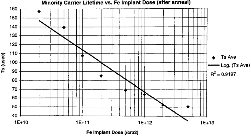
protective oxide into the silicon. It has been reported that Iron concentrations
above IE12
/cm3
inthe siliconlattice begin to degradelifetime [4]. Lifetime was
measured viaSurface Charge Analysis discussed in Chapter 2. The data is shown
in Figure 3. The results clearly indicate a decrease in lifetime
(xmin)
as theiron
Contaminants are introduced into silicon in many ways. The facilities of
most silicon wafer manufacturers are not as clean as the IC fabrication factories
whom
they
supply. Thus contaminants are introduced into the silicon wafersbefore IC devices are manufacturedonthem. Metal alloys such as stainless steel
are popular materials from which the expensive and intricate equipment used for
IC fabrication is constructed. These are excellent sources for contaminants such
as
Iron, Chrome,
Nickel and other alloy metals. The use ofchlorine containinggases and acidsenhances contamination from stainless steels as the passive oxide
film which protects stainless steel breaks down in the presence of chlorine ions
[5]. Chemicals used for cleaning and etching contain small levels of
contaminants. The level of contamination depends on theparticular grade that is
being
used.PPM,
PPB,
and PPT grades contain contaminants in the parts permillion, parts per
billion,
and parts per trillion concentrations, respectively. Thecost ofthese chemicals increases with
decreasing
contamination concentrations.Metalvacuumchucks are usedtoholdwafers
during
processing,placingmetalsindirect contact with the wafer backside. Human interaction with silicon wafers
during
manufacturing is also a major source of contamination. Skinflakes,
direct160 150 140 130 120 5- 11 0)
MinorityCarrier Lifetimevs.Fe Implant Dose (after anneal)
3
.___y _,,
if
^V
<> *S
1 J_v 1
90 80 70 60 50 40
1E+10 1E+11 1E+12
Fe Implant Dose(/cm2)
? Ts Ave Log.(TsAve)
R2
=0.9197
[image:17.511.46.467.32.260.2]1E+13
FIGURE 3: EffectofIron implant doseonminoritycarrierlifetime.
Many
precautions are taken to prevent contaminating silicon wafers.These arenecessary considering the multitude of contamination sourcesthat exist
inthe fabrication area. Some ofthese include clean room suits, face guards, and
gloves to protect from human contact, processing utilizing only high purity
chemicals and gases, and frequent cleaning of vacuum chucks and metallic
components to prevent corrosion. These precautions though necessary are not
sufficienttoprotectIC's fromyieldlossduetocontamination.
Gettering
is a process where contamination is physically orchemically
removed from thecrystalline substrate. The use of chlorine
containing
gasses tochemical gettering. Thisis
typically
done inahightemperaturefurnace wherethereaction products, mainly metal salts, are volatile and removed via the exhaust.
Physical gettering involves
trapping
contamination viathe creation ofcrystallinedefects.
Impurity
atoms within thesiliconlatticewill moveto these defectsites toreduce free energy [6]. Crystalline damage may be created
intrinsically
orextrinsically. Extrinsic gettering occurs when the wafer backsides are
intentionally
damaged. This can be accomplished in many ways. For example,some silicon wafer suppliers depositathin polysilicon filmon thebackside. This
film is filled with crystalline defects which act as gettering sites. In intrinsic
gettering
(IG)
the damage is created internally. This is accomplishedby
utilizingtherelatively high interstitial oxygen concentrationin the silicon wafertoproduce
Si02
precipitates. Precipitate formation produces other effective crystallinedefects such as self interstitials and stacking faults. Figure 4 illustrates the
differenttypesofgettering [6].
This work focused on internal gettering as a mechanism for removing
contamination. In Chapter
2,
the background andtheory
of internal gettering isdiscussed in detail. Experimental procedures for this project are discussed in
Chapter 3. Results anddiscussion arediscussed in Chapter 4. Chapter5
includes
Contaminants
HC1,
TCE
Chemical.
Gettering
I
_ 9 1 __ ?
___-r
i epi. si
Dinuded
J
Zone Intrinsic
Gettering
*
!
Siliconi
Wafer\ Internal defects
Stress. Delects
q^^
*ffftl
ff?
1,
''
7
/r"-/
poly-Si film SigNjfilm
i i i '
i i i
f | |
P diffusion Ign implantationLaser irradiation
Sano-blasting
Mehanical ab'ds>ani
Extrinsic
Gettering
;
J
[image:19.511.84.429.43.423.2]CHAPTER
2
BACKGROUND AND
THEORY
OF
DEFECT CONTROL
IN
SILICON
Silicon wafer substrates contain oxygen incorporated
interstitially
withinthe crystalline lattice. This occurs
during
fabrication ofthe silicon ingotby
theCzochralski
(Cz)
growthmethod[7]. In this method molten silicon(~1410C)
iscontained within a quartz
(SiOa)
crucible. The reaction between the silicon meltand the crucible yields SiO. A portion of the SiO dissolves into the melt and
remainsinthecrystal
forming
an oxygen solid solution with silicon. Figure 5 isa partial phase diagram for the Si-0 system. Typical interstitial oxygen
concentrations,
[O];,
range between 20 and 40 parts per million silicon atoms(ppma). Float zone
(FZ),
another crystal growth method, is used to producesilicon waferswithlittle or nointerstitial oxygen.
Abenefitofinterstitial oxygen in silicon is increased mechanical strength
[8]. Oxygen fills the voids between silicon atoms in the crystal. This produces
lattice strain that makes the crystal more rigid. Silicon wafers with little or no
interstitial oxygen are very brittle. Another benefit is the
formation
ofSi02
precipitates. Contaminants inthe latticeare trapped
by
the precipitates and othercrystalline defects produced when
they
form. Thistrapping
ofcontaminantsby
1400-FIGURE5: Si-O Partialphasediagram[6].
Bulk Defect
Density
vs.[0]i24 26 28 30 32 34
[0]ippma
36 38
[image:21.511.52.403.25.291.2]Figure 5 showsthat as the Si crystal is cooled the solubility ofoxygen in
Si decreases. Precipitation iscaused whenthe solid solution ofoxygen in silicon
becomes supersaturated. A supersaturated solution of oxygen in silicon is
produced whenthe crystal is cooled
trapping
interstitial oxygen before itescapes.Precipitation,
the formation ofSi02
nucleates, may occur in a Si crystalsupersaturated with oxygen. In general, the amount ofprecipitation is related to
the degree ofsupersaturation,
[0]i,
cooling rate, and otherfactors. Formation ofthe precipitates will generate silicon self-interstitials (point
defects)
which are asource of areadefects such as stacking
faults,
dislocationdipoles,
anddislocationloops.
As stated above theamount of supersaturationis dependent upon [0]j. At
low
[O];
the degree of supersaturation required to produce precipitates cannot beattained. Precipitation is not observedbelow a critical
[0]i
of 14 ppma [9].The
relationship between
[0]j
and the amount of precipitation can be explainedby
the
S-curve,
shown in Figure 6. At high[O];
many precipitatesform,
due to thegreater degree of supersaturation. The bulk defect
density
on the y-axis is ameasure of the number of crystalline defects/cm2 on a cross sectional area that
form abouttheprecipitates.
Nucleation refers to the step in which precipitates are first produced. A
precipitate can be nucleated
homogeneously
orheterogeneously.
Homogeneous
oxygen solute. Heterogeneous nucleation results from nuclei formation atlattice
defects such as
impurity
atoms, vacancies,interstitials,
and dislocations.Heterogeneous nucleation is the dominant mechanism at low levels of
supersaturation. Nucleationis athermalprocess which is
typically
performedin afurnace using an inert ambient such as N2. The optimum temperature range for
nucleationhas been showntobe between650C and750C [10].
Formationof a precipitate requires afree energy change,
AG,
as expressedin Equation
1,
[6]
where V represents the volume of the precipitate,AGV
theGibbs free energyper unit volume associated with
formation,
A the surface areaofthe precipitate, and yis the surface energy per unit volume. The two terms in
the parentheses are volume strain energy terms; e is the strain energy per unit
volume oftheprecipitate and
Re
isa strain relaxationterm.AG=-V*AGv+A*Y+(V*e+
Re)
(1)
An infant precipitate is roughly 2.25X larger than theopen space between
atoms in the lattice. Thus a large Gibbs volume free energy is needed to
compensate forthe large strain and surface energies due to the space
limitations.
At the optimum nucleation temperatures (650C
750C)
the siliconlattice
hasrelaxed enoughtoallow theprecipitateto form. At higher temperaturesrelaxation
supersaturation will be less. Thus there is a tradeoffbetween lattice relaxation
andthedegreeofsupersaturation
during
nucleation.Substitutional impurities inthesilicon latticeaffectprecipitation. Dopants
such as Boron push the S-curve toward lower
[0]i
values, thus precipitation ismade easier. This is due to the relative size of the Boron atom compared to
Silicon. Boron is smaller and this creates more open space in the
lattice,
thusthere is less strain and surface energy in the crystal which implies that a lower
Gibbs volume free energy is required for nucleation. This is why heterogeneous
nucleation dominates at a low degree of supersaturation. A larger gap in the
lattice may becreateddueto thepresence ofadefectorimpurity.
Larger
impurity
atoms such as Arsenic have the opposite effect. Theseatoms create more strain and surface energy and shift the S-curve to the right.
Thusalarger Gibbsvolumefreeenergy isrequired forformationof a precipitate.
Electronic device manufacturing requires defect free silicon. Precipitates
candegradeor ruin deviceperformance.Ifa precipitate formsat aP-Njunctionor
at the silicon surface near a gate oxide dielectric layer these structures may be
ruined or prematurely fail.
Additionally,
precipitates may also act as carrierrecombination sites [11]. These problems contribute to both yield loss
during
manufacturing and customer reliability failures. Thus an area of oxygen free
priorto nucleation. Thiswillprevent precipitate formation inthe regionoftheSi
wafer utilized for IC devices. The area of oxygen free silicon is referred to as a
denudedzone(DZ). Theprocess which creates thedenudedzoneis referredto as
denuding.
Denuding
is performed in a furnace at high temperatures (~1000C to1200C)
in an inert ambient(N2
orAr)
with less then 1% oxygen (02). Someoxygen is required to protect the silicon surface from reacting with the nitrogen
due to the high temperature. This oxygen deficient ambient creates a
concentration gradientbetweentheoxygeninthe silicon and thefurnacetube. At
these temperatures the
diffusivity
of oxygen is quitelarge,
thus oxygen near thesilicon surface out diffuses. Figure 7 illustrates calculated oxygen outdiffusion
profiles for several
denuding
processes. All profiles demonstrate the reduction in[O];
nearthe wafer surface.Denuding
time andtemperature are important. Withincreased timemore surface oxygen outdiffuses creating adeeper denuded zone.
Higher temperatures have the same effect, because
diffusivity
increases withtemperature.
Intrinsic gettering
(IG)
is a two stepdenuding-nucleating
process to firstform the denuded zone and secondly, the bulk precipitates. An additional step
maybe requiredtogrow the precipitates larger. An example of such aprocess is
0-o o a >-x o
(1)32 ppma,nopre-heat
(2)28 ppma,nopreheat
(3)32ppma,1150C2Hr (4)28 ppma, 11 SOC 2Hr
[image:26.511.116.419.26.286.2]DISTANCE, pm
FIGURE 7: Simulatedoxygen profiles forvarious
denuding
processes [6].1200 1100 ^ 1000 o a> 3 to 4-a> a. E S 900 800 700 600 IG Process
\
Nucleation/
\
N*
I
|
Denuding
\
/
99.5%Nz
\
J
0.5%02
\
Growth
\
o2
\
oincointtJinojmcMmmmoomT-mTj-^-<T--05cvicNri,r!iri r-;
* co r co t^
c\i ^ co <*
Time(Hours)
[image:26.511.50.457.397.626.2]Nucleation,
the second step in an IG process, is required for precipitateformation.
As stated abovethe optimum temperature ranges between 650C and750C. Inorderforanucleito grow it mustbelarger thanthe critical radius
(rcrit),
which depends on
[0]i
and increases with higher process temperatures. NucleismallerthanrCntwilldissolve into a solid solution. This issummarized in Figure 9.
In IC processing many more thermal steps follow the
denuding-nucleating
cycle. These are the
diffusions,
oxidations, CVD (Chemical VaporDeposition)
processes which are used to build the devices. These processes will affect the
precipitates
depending
on rcrjt.They
could either grow larger or dissolveduring
the high temperature processes such as diffusion and oxidation (~900C
-1200C). Thus the nucleation step must produce some precipitates large enough
to grow at high temperatures. Lower temperature processes (~400C
-800C)
such as LPCVD polysilicon, silicon nitride and oxides will nucleate more
precipitates.
Again,
these precipitates may dissolve or grow larger in highertemperatureprocesseswhichfollow
(depending
oncritical radius). Figure 10illustrates atypical thermal sequenceforanIC fabrication process. Noticethat the
first stepisa
denuding-nucleating
process(InitialOxide).The final wafer cross-section
following
the entire ICfabrication
processshouldpossess adenudedzone nearthesurface andmanybulkprecipitates.
100<H
100
a
1
rx
<
Grow
[Oil,
20 30 40
I
j
J
'
i
/
g
10700 800 000 100Q 1100 1200 1300 1400
TEMPERATURE, C
FIGURE9: Criticalradius vs.
[0]j
and processtemperature [6].1300
1200-
1100-. i i . i I i i ' i i i f ! w r i"
i'
i *
|
t-10 15 20 25 30
J ' '
35 40
111 t '
45 50
[image:28.511.103.421.27.274.2] [image:28.511.59.452.365.638.2]An illustrationof atypicalwafercross-section is shown in Figure 11. Noticethat
the denudedzoneis deeperthan the devicedepth.
Engineering
the denuded zonedepth is important. Ifthe denuded zone is too shallow precipitates may form at
thejunctions of
deep
diffusions(typically
many microns deep). It has also beenreportedthat thebulkprecipitatesservetoisolate IC devices [14]. Ifthedenuded
zone istoo
deep
isolation may be insufficient. Theamountofprecipitationis alsoimportant. Too little precipitation causes insufficient gettering. Too much
precipitation may produce precipitates within the denuded zone.
Gettering
efficiency depends on how much contamination is removed without
impacting
device performance. This is maximized
by
analyzing IC device yield versus theamount of precipitation. Figures 12and 13 illustratedeviceyield versus amount
of precipitation andthe s-curve.
Several techniques canbe utilizedtoevaluate an IGprocess. Electron and
optical microscopy may be used to inspect wafer cross sections for the denuded
zone and bulk defects. A special chemical etch can be utilized to highlight the
defects. The etch preferentially removes silicon in areas ofhigh stress or strain.
FIGURE 11: Wafercross-section withdenudedzone andbulkdefects [13].
Uf
a <o -J
u. u
S ur
U. U
z o 39
I
9r-1
*
M m 0 * M* m p"
2
C9f-3
AMOUNT
OF
PRECIPITATION
(ppma)
20 Ou Cl. O ,o => 5- O-2 5
CHIP YIELD, A.U.
2 3 14
VIELD CURUE
S CURUE
HIGH CARBON
LOW CARBON
3 O 3 S
INtTPAl,"OXYGEN
CONTENT, PPMA
[image:31.511.66.404.33.283.2]4 O
FIGURE 13:
Relationship
between yield,s-curve,precipitation and[OL
[6].ASTMstandardsF 120-75andF121-83 specifyanIRabsorption technique
whichis utilizedtomeasure
[0]i
in silicon wafers[17, 18,
19]. The full width athalfmaximum
(FWHM)
oftheoxygen-in-siliconbandat300K is 312u.m (inwave numbers,32cm'1). Acalibrationconstantrelatedto the absorption
coefficient, a,has been developedthroughtheuse of vacuumfusiontechniques
forthedeterminationof oxygenconcentrationsinsilicon. Theabsorption
coefficient,a,iscalculated viaEquation 2where xdenotes thewafer
thickness,
I0
theinitial
intensity
andIthetransmitted intensity.[O],
at300K isthendeterminedviathecalibrationconstantsinEquations3aand 3b.
a=
(1/x) ln(Io/I)
[0]j
(ppma)
=4.9 a-3
[0]j (cm)
=2.45E17
a(2)
(3a)
Etch Name SCHIMMEL SECCO SIRTL WRIGHT
Etch Composition Stock Solution: Stock Solution: Stock Solution: Mix2g
Dissolve75gCr03in Dissolve44g 50gofCr03to Cu(N03)23H20 sufficientH2O to K2Cr207in 100ml H20. To (reagent grade)
make1000mlof 1000ml H20. To usemix1 part in 60ml H20
solution. Touse use mix1part stocksolutionto (deionized). sampleswith stock solutionto2 1 part49% HF Thenadd(in any
resistivitiesgreater parts49% HF. immediately order): than0.2ohm-cm: priortouse. 60ml 49% HF
mix1part stock 30ml69%HNO3
solutionto 2parts 30ml 5MCr03
49% HF. Tousefor (1gCrCV2ml
sampleswith H2O)
resistivitieslessthan 60mlHac(Acetic
0.2ohm-cm:mix1 acid-galatial)
partstocksolutionto Mixed Wright
2parts49% HF to Etch isstablefor
1.5partsH20. 6weeksatroom
temperature.
Etch Time 5minutesfor
resistivitiesgreater
than 0.2ohm-cm. 15
minutesfor
resistivitieslessthan
0.2ohm-cm.
8-10minutes 3-5minutes 10-15minutes Approximately 6pmremovalof
defectmaterial per5minutes etch.
WaferOrientation <100> <100> <111> <100>or<111>
Dislocations Yes No Yes Yes
SliporLineage Yes No Yes Yes
Swirl Yes Yes Yes Yes
Etch Pits Yes Yes Yes Yes
StackingFaults Yes Yes Yes Yes
Oxygen Defects Yes Yes Yes Yes
Agitation Moderate handor Ultrasonic Moderate hand Moderate hand
[image:32.511.52.464.38.445.2]mechanical ormechanical ormechanical
TABLE 1: Preferentialetch solutions andtheircompositions [16].
FTIR may also be used to determine the amount of precipitation. This is
accomplished
by
measuring[0]i
before and after precipitation(A[O]0
[20].A[0]j
will reflect precipitation because
[0]i
decreases as it reacts with silicon to formSi02. Thus it is not present to affect the absorption coefficient ofthe
Electrical evaluation is done via the
testing
of simple devices. MOScapacitors and diodes can be fabricated utilizingthe IG process. Capacitors can
betestedfor maximumelectrical field
(Emax)
and forced currentbreakdown(Qbd)
ofthe
thermally
grown oxidedielectric. Ifprecipitation occursnearthesurfaceorhigh levels ofcontamination are present the capacitors will leak andbreak down
prematurely.
Many
mechanisms have been suggested for dielectric breakdown[21,22]. Theseare related mostlyto thepresence of charges or chargetrapsin the
oxide or roughness of the silicon surface. Contaminants can produce oxide
charges and traps. Precipitates can cause roughness of the silicon surface.
Dielectric breakdown is broken into 3 modes. These are
A, B,
or C mode. Amode breakdowns are categorized
by
avery low breakdown field. This may bedue to a direct short or pinhole through the dielectric. C mode breakdowns are
associated with the maximumfield
theoretically
allowedby
the dielectric. For agood thermaloxidethis isnear 10 MV/cm. B modefailures arebetween A andC
modes. Forathermaloxidethis is between 3 and7 MV/cm. Capacitance-voltage
(CV)
testing
can be utilized to measure the amount of oxide charges and traps[23]. Capacitance-time
(C-t)
and Zerbst analysis are used to determine minoritycarrier lifetime
(Xmin) [24],
which is related to carrier recombination-generationandmay be usedtodeterminethelevelof contamination orprecipitation. Surface
Charge Analysis
(SCA)
is another technique that can be employed to evaluatecharges, traps and Tmin [25]. SCA makes use ofthe surface photovoltage
(SPV)
response to a DC bias capacitively applied to the silicon substrate. In this
Diodes can be tested for junction leakage and breakdown. Increased
leakage and premature breakdown can be attributed to contamination or
precipitation at the P-N junction [26].
Additionally,
the diodeideality
factor(n)
can be used for evaluation. The
ideality
factor is calculatedby
measuring theslope in the I-V curve formoderate levels offorward bias [27].
Recombination-generation mechanisms due to contamination can affect the
ideality
factor. Thevalue ofn shouldbenear oneforahigh quality diode. Theextraction of nfroma
diode I-Vcurveis summarizedin Equation 4where
kb
is Boltzmann's constant, qis the electron charge and T is temperature in Kelvin.
Vi, V2,
Ii
andI2
are thevoltageandcurrent measurementsfromtheI-Vcurve.
n=
(q/kbT)
*(V2
-Vx)
/ln(I2
/Ii)
(4)
Another method used to evaluate an IG process is to study the I-V
characteristics of MOStransistors. Comparisonscanbemadebetweentransistors
fabricated with and without the use of the process. Subthreshold slope
measurements determine the amount of carrier recombination or leakage that
occurs while the transistors are in the OFF state [28]. Transistors with a greater
subthreshold slope indicate a higher recombination rate. This is related to the
amount of contamination. The I-V characteristics of the transistors in the ON
state can also be compared. Leakage due to contamination will
degrade
theThisresearch focusedonengineeringthe surface andbulk defect densities
insingle crystal silicon viainternal getteringtoenhance theelectricalperformance
of gate oxides and P-Njunctions subsequently fabricated in the surface regionof
thecrystalline substrate. Chapter 3 covers theexperimental procedures employed
in
developing
and characterizing the IG process, and Chapter 4 presents theCHAPTER
3
PROCEDURES
Thisproject was organizedintothreephases. Phase 1 involved
developing
an IG process compatible with the silicon substrates and equipment at RIT.
Electrical evaluation ofMOS capacitors and P-N junction diodes fabricated with
and without the IG process was accomplished in phase 2. The original goal of
phase 3 was to study the effects of the IG process on subthreshold and I-V
characteristicsofMOS transistors. After completing phase2 itwas apparentthat
the diodessuffered fromparasitic effects due topositive charge inthe fieldoxide.
Thisproducedabnormally high leakage currents whichmaskedthebenefits ofthe
IG process. Therefore the revised goal of phase 3 was to repeat the diode
evaluation
by
making changes to the fabrication process which eliminated theparasiticleakagecurrents.
PHASE1 - IG PROCESSDEVELOPMENT
A small study was performed to determine the optimum nucleation
temperature. As previously mentioned, references indicated this temperature
somewhere between 650 and 750C. Therefore temperatures of
650,
700 andnucleation time was 4 hours. One boron doped p-type
(Na
~ 1 X 10 cm),
<100>, wafer was cleavedinto quarters andscribedfor later identification. Prior
to cleaving, the wafer received a buffered oxide etch
(BOE)
and spin rinse/dry.One quarter was nucleated in
N2 (5slm)
at each temperature in the furnace tubeused forgateoxide growth. The fourth piece was kept for Infrared
Spectroscopy
(IR)
measurements of[0]j.Following
nucleation the threenucleated wafer pieceswere processed together at 1050C for 5 hours in
dry
02
(5 slm) to grow theprecipitates larger. Figures 14 and 15 summarize the furnace thermal cycles.
Following
growththeoxide was removed viaaBOEdip
and spin rinse/dry. Thesampleswere subsequentlycleavedinto smallerpieces toexposethe wafer
cross-section. A Wright etch was mixed and used to highlight the precipitates in the
cross sections. The etch composition is located in Chapter
2,
Table 1. Thesamples were etched for 10minutes, rinsedin DIwater, anddriedvia an
N2
gun.The samples were inspected
by
optical and scanning electron microscopy andmicrographs were acquired via both instruments.
Later,
an IR measurement of[0]i
was completed on the fourth piece at the Motorola MOS 3 IC fabricationfacility
inAustin,
Texas.Following
the nucleation study a twofactor,
three level factorialexperiment was designed to study the effects of combining
denuding
andnucleation. The two factors were denudation time and nucleation temperature.
UI rr D
\
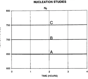
UJ 0-800 750 700 650 600 NUCLEATION STUDIES N2c
RA
1 2 TIME(HOURS)FIGURE14: Nucleation studythermalcycles.
NUCLEATION GROWTH 1100 ~ 1050 1000 950 900 850 800 750 700 LU cr ID
\
UI O-UI 3 4 TIME(HOURS) [image:38.511.110.410.58.329.2]summarizes the factors and their
levels,
and Table 3 contains the groupinformation fortheresulting9runs.
DenudingTimeat1 100C Nucleation Temperature (4hours)
2 hours 650C
6 hours 700C
10 hours 750C
TABLE 2: Two
factor,
three level factorialexperimentaldesign.GROUP DENUDE @
1100C
NUCLEATE(4
HOURS)
A 2HOUR 650C
B 2HOUR 700C
C 2HOUR 750C
D 6 HOUR 650C
E 6HOUR 700C
F 6 HOUR 750C
G 10HOUR 650C
H 10 HOUR 700C
1 10HOUR 750C
TABLE3:
Group
versusIG process.Three boron doped p-type substrates similarto that used inthe nucleation
study were obtained and cleaned using a BOE
dip
and spin rinse/dry. Eachsubstrate was cleaved into four quarters and scribed. Special care was taken to
identify
thesamples withthewaferfromwhichthey
came. Thiswastoinsure
thatthree wafers. One samplewas randomlyassigned toeach run ofthe experiment.
One piece from each wafer was saved for subsequent
[0]i
measurements.Denuding
was performed in the gate oxide tube using a gas mixture of 95%N2
and 5% 02. A more dilute oxygen mixture was desired but this ratio was more
reasonable due to limitations inthe
02
flow meter. In order fortwo gases to beused simultaneously in the oxidation tube an
N2
rotometer was installed. Theflow rates were 15slm
N2
and 0.75slm 02.Only
threedenuding
runs wererequired due to
blocking
in the experimental design. Three samples each weredenuded at 1 100C for 2
hours,
6hours,
and 10hours respectively. The sampleswere introduced into the furnace at 800C before ramping to the
denuding
temperature. This was toprevent nucleation priorto
denuding,
which may resultinprecipitatesthatwouldhave been largeenoughto growinsteadofdissolving.
Nucleation was performed in the same tube
following
denuding.Again,
only three runs were required due to blocking. The samples, one each from the
denuding
cycles, were nucleated for 4 hours in 5slmN2
at650,
700,
and750C,
respectively. A three step cycle was utilized to grow the precipitates. This
consisted of2 hours at 1000C in
dry
02
followedby
5 hoursat 1050C inN2
andcompleted at 1 100C in
N2
for 2 hours. Duetoprogrammingandtimeconstraintswith the furnace equipment, the three steps were completed separately and
included performing thepush/pull at 800C and ramp up andramp down cycles.
Because of the relationship between rcnt and temperature it was
believed
thatby
have abetterchance ofgrowing insteadofdissolving. Thisthermal sequencemay
not always be thecasein aconventional IC process. The thermal cycles for this
experimentplusgrowth aresummarizedin Figures
16, 17,
and18.Following
the growthcycletheoxidewasremoved fromthe samplesvia aBOE etch. The samples were rinsed in DI H20 and blown
dry
with N2. Thesamples werethen cleavedinto smaller pieces toexposethe wafercross sections.
A 10 minute Wright etch was performed followed
by
DI H20 rinse andN2
dry.The cross-sections were inspected via optical microscope and
SEM,
and bothoptical and electron micrographs were taken.
Later,
IR measurements werecompleted todetermine
[0]i
on all samples(including
theinitial 3 wafers forthenucleation study) at the Motorola MOS 3 IC fabrication
facility
inAustin,
Texas.Thepictures anddatawere usedtoselect an optimumIGprocessforuseinphases
2 and3. Analysis included determination ofthe denuded zone depth
(DZD)
andbulk defect
density
(BDD cm"2). The chosen IG process was to be the 6hour,
1150 1100 1050 o UI rr 1000 ->
$
950 UI Q. 900 III h-850 800 750DENUDING CYCLE BY GROUP
95% N2
5%Q?
N2J
\
\\ \
1
\
\ \1
\
\\
I
\
\
\ \
1
\
\ \1
\
\ \1
\
i il_
\
\ \Y_
\
\i
\
A,B,C D.E.F G,H,I
4 6 8
TIME(HOURS)
[image:42.511.99.411.387.601.2]10 12
FIGURE 16: IGprocess
development, denuding
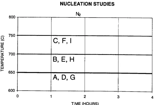
cycles.800 -. 750 O ui rx UI Q. UI 700 650 600 NUCLEATION STUDIES
C.F.I
B.E.H
A,D,G
TIME(HOURS)1150
1100
1050
O
w 1000
rx
Z>
rl 950
ui
I
900l-850
800
750
PRECIPITATEGROWTH- ALL GROUPS
O2 N2
6 8
TIME(HOURS)
[image:43.511.47.428.103.345.2]10 14
FIGURE 18: IGprocess
development,
growth cycles.PHASE 2 - MOS CAPACITOR ANDDIODEEVALUATION
It was decided that three conditions would be utilized in the diode and
capacitorfabrication. These included fabrication withouttheIG process, withthe
IG process, and with nucleation only (no denuding). As stated earlier a 6
hour,
1 100C denude and 4
hour,
700C nucleation were selected for the IG process.the device regions. Two device wafers were processed for each IG condition.
Thus atotalof12wafers wererequired(6capacitorand 6diode).
Diode processing was accomplished using an existing 4 level metal gate
PMOS mask set. The mask set included the RIT PMOS test chip [29].
Only
levels
1,
3 and 4 were required for diode fabrication. These werediffusion,
contactcut, and metal, respectively. The PMOS process atRIT is designed tobe
fabricated on an n-type substrate [30]. The substrate contact requires aluminum,
and sintered aluminum contacts to n-typesubstrates produce adiode. This is not
desirable for an ohmic contactand would have created a parasitic diode in series
withthedesigneddiode. To achieve an ohmic contactbetween aluminum and
n-typesubstratean additionaln+regionisrequiredinthecontact areas.
Conversely,
aluminum to p-type substrate produces an ohmic contact.
Thus,
theprocess wasmodified for the use of p-type substrates and n-type
doping
to yield n+ to psubstrate diodes. Aluminum was deposited on the wafer backsides for substrate
contacts.
Several diodes have been designed into thetest chip, four of which were
targetedfor
testing
after fabrication.They
were labeled diode 1 through diode4,
andtheirlayouts are shownin Figures 19 and 20. Diodes 1 through 3 possessed
the smallest diffusion areas.
They
were15K, 6K,
and 16K u.m2, respectively.Diode 4 was the largest at 80.5K |im2. All were square or rectangular except
MOS capacitor fabrication was accomplished via the use of a capacitor
test mask. This mask yielded round and square capacitors ranging in area from
100Kto2M um2. Aluminumwas deposited over gate oxideon p-type substrates
to produce the MOS structure. Aluminum was also deposited on the wafer
backsides for substrate contact after a BOE step was performed to remove the
backsideoxide. The front sideofthe waferwasprotected withphotoresist
during
thisstep.
Twelve boron doped p-type (Na ~ 1 X IO15
cm-3), <100> wafers were
obtained. The capacitor and diode wafers were scribed numbers 1 through 6.
Two wafers foreach device were randomly selected for eachIG condition. The
waferassignmentsaresummarizedinTable 4.
IG Condition Capacitor Wafer # Diode Wafer #
No Getter 4,6 1,6
Getter 2,5 3,5
NucleateOnly 1,3 2,4
w**mmmmJA
[image:46.511.128.398.18.263.2]7
FIGURE 19: Metal gatePMOSdiode
design,
diodes1,
2,
and3 (1to r). Diode1is between pads1 and7. Diode 2 is betweenpads2and8. Diode3is
betweenpads 3and9.
g^i^^MJ
5^?I
*m
I
[image:46.511.178.334.396.580.2]Following
scribe all wafers were RCA cleaned. The clean sequenceconsisted ofAPM (ammonia/hydrogenperoxide mixture) heatedto 75 C for 10
minutes, cascade DI
rinse,
50:1 HF 30 seconds, cascade DI rinse, HPM (HC1peroxide mixture) heated to 75C for 10 minutes, cascade DI rinse, and spin
rinse/dry. Lowparticulate cleanroomgradechemicals were used. The RCA bath
composition and mixtures are located inTable 5. Special attention was given to
thechemicaltanks. Eachtankwas rinsedtwice then allowedto sitovernight ina
dilute HC1:DI water mixture. This was to minimize contamination from the
chemical clean.
Bath DIwater Peroxide Acid/Base
APM 4700ml 1000ml 100mlNH4OH
HPM 4700ml 1000ml 100mlHC1
TABLE5: RCA clean mixtures.
Following
RCAcleanthedenuding
cycle was performedin the gate oxidetube. The wafers were loaded flat up and pushed into the tube at 800C in 5slm
N2
at 12 inches/minute.Only
the capacitor and diode wafers whichrequired theentire IG cycle were processed. The furnace was ramped to 1100C in the 95%
N2,
5%02
mixture (15slmN2
and .75slm02)
using the02
flow meter andN2
rotometer setup. Aftera6 hoursoakthefurnace was cooled to
800C
in 5slmN2
(tri-chloroethane) clean was performedonthe tube and a new quartzboat at 1 125C
for 4 hours. Thiswas doneto removeas muchmetalliccontamination aspossible
fromthefurnaceandboat
by
utilizingthechlorinein TCA toreact with metals toforma salt. At hightemperaturesthesalt isvolatile and removed viatheexhaust.
The nucleation-only wafers were merged with the denuded wafers and all were
nucleated in the gate oxide tube at 700C for 4 hours in 5slm N2.
Following
nucleationthe oxidethickness on the denude-nucleated wafers was measured via
Nanospec. Surface Charge Analysis
(SCA)
was performed on bothdenude-nucleatedand nucleatedonly wafers. Oxide on thedenude-nucleated wafers was
thenremovedvia aBOEetch and spinrinse/dry.
All wafers were RCA cleaned in preparation for the 5000A wet
pattern/field oxidation. The wafers were loaded flat up and pushed at 800C in
5slm N2. The furnace was rampedto 1000C in 5slm
dry
02. Thewet oxidationwas performed
by flowing
5slm02
gas through a bubbler containing DI H20heated to nearboiling. The oxidation timewas 90 minutes. After oxidation the
furnace was ramped to 1050C in 5slm
N2
for a 1 hour anneal.Following
theanneal the furnacewas cooled to800C andthewafers pulled in5slmN2. Oxide
thickness and SCA measurements were then performed. Besides growing an
oxidenecessarytofabricate electricaldevices thisprocess also servedto growthe
Diffusion
lithography,
oxide etch, and n+ implant were completed on thediode wafers using level 1 ofthe metal gate PMOS mask set. This consisted of
coating thewaferswith
Shipley
812 positive photoresist, exposing on a GCA 5Xg-line stepper at an energy of
180mJ/cm2,
anddeveloping
inShipley
MF321developer. After
development
the n+ areas wereopen inthephotoresist coatings.A BOE etch was performedto remove the field/pattern oxide over the n+ areas.
Theetchtimewascalculated assumingan etchrate of1000
A/minute
and includeda25% overetch.
Following
theetch and spinrinse/dry
an inspection verified thattheoxide hadbeenremovedin then+ areas. The n+ implant was completed ona
Varianlowcurrent ion implanter. Aphosphorous dose
(singly
charged, 3 1AMU)
of
5xl015 atoms/cm2
at HOKeV was performed to establish the n+ regions
Following
the implant a 50 minute 300 Watt plasma02
ash removed photoresistfromthediodewafers.
All wafers received an implant anneal to activate the dopant and restore
crystallinity. An RCA clean was necessary prior to the anneal. The wafers were
pushed at 800C in 5slm
N2
and the furnace ramped to 1100C for a 15 minutesoak.
Following
thesoakthefurnacewasrampedto 1000C in 5slmwet02
for a10 minute oxidation. After oxidationthefurnace was rampedto900C in 5slm
N2
andthewafers pulled.
The diodewafers were again loaded into a
furnace
at 800C in 5slmN2
tosimulate the thermal sequence ofthe thin gate oxidation that the capacitor wafers
would receive.
Heavily
doped material such as the diode wafers should not beprocessed inthegate oxide furnace asthedopants may outdiffuse
during
the slowgrowth andcontaminatethetube. Thus the thermalcyclehadto besimulatedin a
another tube. The temperature wasramped to 1000C fora20 minute soak. The
furnace was then cooled to 800C and the wafers pulled.
Following
the thermalcycle nanospec oxide thickness measurements were made in the field and n+
areas.
Thin gate oxidation was performed on the capacitor wafers. The target
thicknesswas250A. Priortooxidationthe tubeandthequartzboatwere 02/TCA
cleaned at 1100C for 4 hours. The wafers were BOE etched to remove the
field/pattern oxide and RCA cleaned. The gate oxide process consisted of a
800C push in 5slm
dry
02/TCA. The furnace was then ramped to 1000C in5slm N2. Aftertherampa5minute oxidationwasperformedin 5slm
dry
02/TCAandfollowed
by
another 15 minutesin 5slmdry
02. The furnacewas then cooledto 800C in 5slm
N2
and the wafers pulled. Oxide thickness and SCAmeasurements were completed.
Contact
lithography
and oxide etch were completed on the diode wafersusing level 3 ofthe metal gatePMOS mask set. After
lithography
both n+ activeand substrate contactswere openin the photoresist coatings. The field and active
oxide was removed via a BOE etch. The etch time was calculated for the
field
assumed. An
02
plasma ash was utilized to remove photoresistfollowing
theetch.
Aluminum was deposited onto both the capacitor and diode wafers via
evaporation. The diode wafers received a 30 second 50:1 HF
dip
and spinrinse/dry
prior to deposition in order to remove any native oxide from thecontacts. An Al/Si alloy was usedforthe diode wafers to prevent spiking ofthe
n+ to p junctions. Pure aluminum was used for capacitor wafers. Evaporation
was preferred over sputtering for the capacitor wafers because all efforts were
made to avoidexposing the thinoxides to potentially
damaging
plasmaradiation.Thetarget thickness was5000Aof aluminum.
Metal
lithography
and etch were completed on the diode wafers usinglevel 4 ofthe metal gate PMOS mask set. Capacitors were defined via the RIT
capacitor test mask. A heated
(50C)
wet metal etch solution was utilized toremove aluminumleftunprotected
by
photoresist. Theetch was completed whenthe bubbles disappeared from the wafer surfaces and the metal lines became
visible. Photoresist was removed from the diode wafers via a plasma ash. Wet
solvents were used to remove photoresist from the capacitorwafers.
Again,
thiswasto avoidpotentially
damaging
plasma radiation.Pure aluminum was evaporated onto the
backsides
of the capacitor anddiode wafers. Prior to deposition the wafer
frontsides
were coatedprotective layerof resist while oxide was removed fromthebacksides via aBOE
etch. Theresist was ashedfromthediodewafers anddissolved
by
solventsonthecapacitor wafers. Thealuminumtarget thicknesswas2500A.
The diode and capacitorprocessing was completed
by
a 15 minute 425 Csinter in
forming
gas (H2/N2). Phase 2 capacitor and diode process data arelocated in Appendix A.
Following
sinter the devices were ready for electricalevaluation.
Dielectricstrengthofthecapacitor was determined viadestructive electric
field breakdown
testing
using a HP4145 parameter analyzer.Testing
wasperformed on
800Ku,m2
and
2M(im2
square shaped capacitors. A standard test
pattern was established in orderto gather comparable data between capacitors on
different wafers and
having
various IG fabrication conditions.During
the test,current was monitored while a constant voltagerampwas appliedtothecapacitor.
Voltage was applied to the gate such that the substrate was in accumulation.
Breakdown was measured at the voltage where current reached 1mA.
Dividing
the breakdown voltage
by
the oxide thickness yielded the electrical field. Themostcommonly used unit for field breakdown is MV/cm. Leakage current prior
to destructive dielectric breakdown on
2Mum2
capacitors was determined via a
similar test on the HP4145. Current was measured at a bias of 25 volts.
Histograms were created to
identify
variations in thebreakdown
andleakage
A, B,
orC,
where Amode failures represent directshorts, B mode are midrange,andCmode nearthemaximumdielectric strength.
C-V
testing
was completed onlOOKum2
circularcapacitors via a
Keithly
simultaneous high frequency/low
frequency
system. Total oxide charge andinterface
trap
density
at midgap data were collected. Additionally, plots ofinterface
trap
density
versustheband gapwere generated. C-tandZerbstanalysiswas also performed using the
Keithly
apparatus. This provided carrier lifetimedata.
Reverse bias leakage
testing
on diodes 1 and 3 was accomplished on theHP4145. This test is similar to the capacitor tests in that current is measured
versus a voltage ramp. For diode 1 thecurrent was measured at 50volts reverse
bias. Diode 3 leakage was measured at 30 volts reversebias due to thedifferent
design geometry.
Again,
a standard test pattern was utilized for comparisonsbetween different wafers and IG conditions. Histograms were used to
identify
differences indistributions.
Ideality
testing
was performed on diode 1 utilizing the HP4145. Thelog
of the current was plotted versus voltage just prior to the turn on voltage (-0.6
volts). Theslope of a linefit totheexperimental curve yielded the
ideality
factorResistance measurements were made on diffused resistors to verify that
the variations in
leakage,
breakdown andideality
were not due to differences inthe
doping
or sheet resistance acrossthep-njunctions.PHASE 3 - DIODE OPTIMIZATIONAND FURTHER EVALUATIONS
Large leakage currents were evident for the diodes fabricated in phase 2.
Upon furtherconsideration itwasrealized that theleakagewasdueaninadvertent
inversion ofthep-type wafer surfaces. This was due to thehigh level ofpositive
fixed charge in the oxide from the wetoxidation and segregation ofboron from
the substrate into the oxide which produces a
lightly
doped surface region. Thepositive fixed charge repelled the majority holes and attracted minority electrons.
Enough electrons were attracted to the surface
by
the positive oxide charge thattheregion of silicon atthewafer surface becamen-type. This inversion layer may
produce avariety of effects. Ifthe p-contact of the diode is the wafer
backside,
the inverted surface region may act as a source of minority carriers which may
"spill"
into the diode depletion region and increase leakage current. If the
p-contactisonthefrontside, theinversion layer acts as ahighconductance channel,
in parallel with the
diode,
which will increase the total measured current. Thechannel also makes the Si02/Si interface part of the "active"
device,
thusinvolving
the interface traps and surface recombination velocity phenomenon.oxide
charge
substrate
n+contact contact
\-/~\
rvi
Al
/
_1_\A1
+ + +
FieldOx\M
j
+
O O 000
\
/<3Q<3 <=>~ *^~~
"Z^P
\
n+/
minoritye
psubstrate
[image:55.511.118.394.50.265.2]~
substrate contactFIGURE 21: Cross section
illustrating
parasitic problems on phase2n+on p diodes.
SUPREM 3 process simulations and electrical threshold voltage extraction
of the parasitic MOS transistor were performed. This indicated a threshold
voltage of approximately -12 volts. Reverse bias
testing
requires that the n+diffusions and aluminum connections be biased positively with respect to the
substrate. ThustheparasiticdeviceswereON.
Modificationsweremadeto then+onp substratediode
fabrication
processto minimize theeffects of positive field oxide charge andboron segregation. This
included the addition of a
BF2
"field Vt adjust"implant
prior tofield/pattern
oxidation. This increased the surfaceboron concentration. The
implant dose
was8xl013
cm"2,
BF2
at lOOKeV. A 1 hour 1100C anneal was added to thefield/pattern oxidationbefore the 1000C wet ox stepto diffusetheboron implant
deeper into the silicon and reduce the loss due to the oxidation. SUPREM 3
simulations revealed an improved parasitic threshold voltage ofapproximately 14
volts
indicating
theareaunderthefieldoxide was no longer inverted.Additionally,
on ndiodeswerefabricated alongwith the modified onp diodes utilizingphosphorous doped
(Nd
~ lxl015
cm"3) <100> substrates. The
p+regions wereformedviaimplantationof
BF2
atthe samedoseand energyasthen+ implant. Thep+on n diodes didnot require an additional implant for the field
thresholdbecausephosphorous doesnot segregate intothe oxide. Ann+backside
implant was added to produce an ohmic contact with aluminum. The dose was
3x1015 cm"2
phosphorous at HOKeV. Both diode types were processed together
exceptforthen+orp+implants.
The diodes werefabricated with and without the IG process. Each group
consisted oftwo wafers each. Thus atotal of8 wafers were processed, 4 p-type
and 4 n-type. The wafer assignments are located in Table 6. Process data for
phase3
diode
fabrication islocated
inAppendix B.IG Condition n+onpwafer# p+on nwafer#
NoGetter 2,4 1,4
Getter 1,3 2,3
Electrical evaluation was similar to phase 2. Diode 4 was utilized for
reversebias leakage measurements onboth diodetypes. The larger junction area
was more susceptible to leakage and other anomalies due to contamination. For
thep+ on n diodesleakagewas measured at60volts reversebias. Leakageonthe
n+ on p diodes was measured at 10 volts reverse bias. The difference in reverse
bias measurements is due todifferent
doping
across thep-njunctions for the twodiodetypes.
Ideality
testing
for both diodetypeswasaccomplishedusing diode 1.Reverse bias breakdown ofthep-njunctions was alsodetermined. Forthe p+ on
n diodes this was the voltage required to produce 1mA of current. The n+ on p
diodes broke down at a much larger reverse bias voltage. Breakdown was
measured as the voltage required to produce lOOuA of current. Resistance
measurements were made on diffused resistors to verify that the variations in
leakage,
breakdownandideality
were notduetodifferences in thedoping
or sheetCHAPTER
4
RESULTS AND DISCUSSION
As stated in Chapter 3 this project was organized and performed in three
phases. Inthischaptertheexperimental results arepresentedforeach stage along
with the corresponding discussion of the results. Chapter 5 will state th
![FIGURE 4: The various forms of gettering [6].](https://thumb-us.123doks.com/thumbv2/123dok_us/61932.5777/19.511.84.429.43.423/figure-the-various-forms-of-gettering.webp)
![FIGURE 6: Example of precipitation s-curve. Bulk defect density vs. [0]i [6]](https://thumb-us.123doks.com/thumbv2/123dok_us/61932.5777/21.511.52.403.25.291/figure-example-of-precipitation-curve-bulk-defect-density.webp)
![FIGURE 7: Simulated oxygen profiles for various denuding processes [6].](https://thumb-us.123doks.com/thumbv2/123dok_us/61932.5777/26.511.50.457.397.626/figure-simulated-oxygen-profiles-various-denuding-processes.webp)
![FIGURE 10: Thermal sequence of example IC fabrication process [12].](https://thumb-us.123doks.com/thumbv2/123dok_us/61932.5777/28.511.103.421.27.274/figure-thermal-sequence-of-example-ic-fabrication-process.webp)
![FIGURE 11: Wafer cross-section with denuded zone and bulk defects [13].](https://thumb-us.123doks.com/thumbv2/123dok_us/61932.5777/30.511.84.442.335.607/figure-wafer-cross-section-denuded-zone-bulk-defects.webp)
![FIGURE 13: Relationship between yield, s-curve, precipitation and [OL [6].](https://thumb-us.123doks.com/thumbv2/123dok_us/61932.5777/31.511.66.404.33.283/figure-relationship-yield-s-curve-precipitation-ol.webp)
![TABLE 1: Preferential etch solutions and their compositions [16].](https://thumb-us.123doks.com/thumbv2/123dok_us/61932.5777/32.511.52.464.38.445/table-preferential-etch-solutions-compositions.webp)