Continuous-wave highly-ef
fi
cient low-divergence
terahertz wire lasers
Simone Biasco
1, Katia Garrasi
1, Fabrizio Castellano
1, Lianhe Li
2, Harvey E. Beere
3, David A. Ritchie
3,
Edmund H. Lin
fi
eld
2, A. Giles Davies
2& Miriam S. Vitiello
1Terahertz (THz) quantum cascade lasers (QCLs) have undergone rapid development since their demonstration, showing high power, broad-tunability, quantum-limited linewidth, and ultra-broadband gain. Typically, to address applications needs, continuous-wave (CW) operation, low-divergent beam profiles andfine spectral control of the emitted radiation, are required. This, however, is very difficult to achieve in practice. Lithographic patterning has been extensively used to this purpose (via distributed feedback (DFB), photonic crystals or microcavities), to optimize either the beam divergence or the emission frequency, or, both of them simultaneously, in third-order DFBs, via a demanding fabrication procedure that pre-cisely constrains the mode index to 3. Here, we demonstrate wire DFB THz QCLs, in which feedback is provided by a sinusoidal corrugation of the cavity, defining the frequency, while light extraction is ensured by an array of surface holes. This new architecture, extendable to a broad range of far-infrared frequencies, has led to the achievement of low-divergent beams (10°), single-mode emission, high slope efficiencies (250 mW/A), and stable CW operation.
DOI: 10.1038/s41467-018-03440-4 OPEN
1NEST, CNR—Istituto Nanoscienze and Scuola Normale Superiore, Piazza San Silvestro 12, 56127 Pisa, Italy.2School of Electronic and Electrical Engineering, University of Leeds, Leeds LS2 9JT, UK.3Cavendish Laboratory, University of Cambridge, Cambridge CB3 0HE, UK. Correspondence and requests for materials should be addressed to M.S.V. (email:[email protected])
123456789
combined with new laser resonator concepts, have recently enabled the control and confinement of electron and photon paths in optoelectronic devices with an unprecedented degree of control. For example, microcavities4, photonic crystals5,6, and both pseudo-random7,8 and random9 photonic structures, can manipulate and confine light in small volumes, and at targeted frequencies. This has further expanded the functionality of the THz QCL, allowing operation at a single emission frequency7or over a broad (0.5 THz) frequency bandwidth, or with designed directional beam patterns8.
These approaches rely on lithographic patterning of the top metal waveguide surface, which enables the guided mode to be matched to the externally propagating photons, generating a collimated beam from the laser surface by interference. In a one-dimensional periodic structure with surface periodicity Λ, light extraction can be tailored on the fundamental (m=1) spatial harmonick1=1/Λ of the grating, while optical feedback inside
the resonator is provided by a wavevector with km=m/Λ10.
Based on the order m of the feedback wavevector, one-dimensional distributed feedback (DFB) structures11–13 can be engineered to provide directional emission over a specific plane, governed by the interaction between the light wavevector and the feedback wavevector14.
In these architectures, high-power emission, beam shaping, and mode control are related to the extraction of symmetric and anti-symmetric resonant eigenmodes. In general, symmetric modes produce constructive interference in the far-field and have efficient outcoupling into free space. In contrast, anti-symmetric modes interfere destructively in the far-field, but have lower loss. As such, anti-symmetric modes are favored for lasing, but con-sequently provide limited extraction power. A number of pho-tonic approaches have been explored to circumvent these intrinsic limitations, while still ensuring directional beam profiles. These include vertically emitting graded photonic hetero-structures15,16, quasi-periodic gratings17, and double-periodicity DFB gratings, engineered to achieve a simultaneous tailoring of the emission frequency and a tuning of the beam direction, via the independent control of the extraction and feedback wave-vectors18. Further approaches have utilized on-chip phased locked arrays19,20 and metasurface reflectors, which comprise multiple cavities21, and induce directional THz QCL emission in pulsed operation.
In contrast to surface-emitting approaches, edge-emitting structures with narrow cavity widths are potentially more suited for applications in sensing, spectroscopy or metrology due to the lower electrical power dissipation, which better enables continuous-wave (CW) operation. In-plane emitting wire lasers exploiting third-order DFB gratings20,22,23, and including inte-grated micro-antennas24, are the most exploited solutions in this respect. Despite the clear advantages in the emission profiles (10° divergence)20,22 and slope efficiencies (120 mW A−1) these
odicity of the array of surface holes is not an integer multiple of the lateral corrugation controlling the feedback. The feedback grating selects the lasing frequencies and allows robust single-mode emission, exploiting the inherently high spectral purity of THz QCLs26, while the extraction array isfinely tuned to opti-mize the radiation outcoupling. This architecture thereby simul-taneously addresses the challenges of low-divergence, single-mode emission, high power, very good slope efficiency, also in CW regime.
Results
Device concept and architecture. Our photonic wire design was
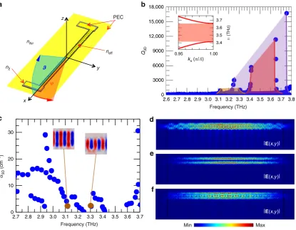
conceived to provide independent control of the feedback and extraction mechanisms through use of two independent photonic geometries. To ensure the necessary feedback for radiation pro-pagating in the resonator, a one-dimensional photonic grating is implemented by defining a lateral sinusoidal corrugation, which modulates the width of the 10-μm-thick double-metal QCL cavity (Fig. 1a) in the 30–50 µm range. Consequently, the resonator width is comparable to the typical THz wavelength in a GaAs/ AlGaAs-based QCL material (~30 µm for 3 THz radiation), making the system an almost perfect one-dimensional photonic structure. The spatial Fourier transform of the corrugation peri-odicityΛfb(Fig.1a) defines a feedback wavevector, which is twice
the light wavevector in the active material. Setting the emission frequency to 3.1 THz, the feedback wavevectorkfb=2neffν/c(with
cthe speed of light in vacuum andνthe desired laser frequency) corresponds to a design corrugation periodicity Λfb=13.6 µm,
assuming an effective refractive index of the active region metallic waveguide neff=3.53, as derived from the simulation of the
transverse propagation of the fundamental mode in a two-dimensional slab27.
Light extraction into free space is controlled by a second grating: an array of circular holes lithographically defined on the top surface of the laser. The underlying semiconductor hetero-structure is left exposed after removal of the upper metallic waveguide, and also the n+top contact layer (by dry-etching) to prevent detrimental absorption of the outgoing radiation (Methods section). The surface holes have a diameter of 10 µm (Fig. 1a) while their periodicity, Λe, is designed to induce a
longitudinal outcoupling of the radiation with an emission angle
ϑ=90° with respect to the surface normal (Fig. 1b). The one-dimensional light cone diagram in Fig. 1b provides a simple description of the scattering between the light, the feedback and the extraction wavevectors.
When a guided mode propagates inside the resonator with wavevectorneffk0(black arrow in Fig.1b), it is scattered by the
feedback vectorkfb(red arrow in Fig.1b) in the opposite direction
periodicity. By carefully tuning ke, the resulting diffracted mode
can match the light wavevector in air, meaning that the vector sum of the three wavevectors must intercept the free-space light cone (blue dashed circular line, Fig.1b) with radiusk0=ν/cat its
bottom corner. Consequently, the value of the extraction wavevector (Methods section), required for longitudinal emission is given by:
ke¼ν
cðneffþsinϑÞ ¼ν
cðneffþ1Þ ð1Þ
which determines the scattering matching condition and the periodicity Λe. By using the parameters introduced earlier, the
extraction periodicity was set toΛe=21.2 µm.
Since the frequency-dependent effective refractive index can be engineered by design in a QCL, we can obtain a perfect matching condition by tuning the extraction wavevector, by spanning a 10% range around the light cone edge. To achieve this, a series of wire lasers incorporating surface hole array of different periodicities were lithographically defined to achieve a sequence of different extraction wavevectorsηke(withηin the range 0.9 <
η< 1.1, in steps ofΔη=0.05). This allowed the investigation of the optimal scattering condition, for which light extraction is enhanced and emitted in the desired direction, with low-divergence and large quantum efficiency.
The resonator geometry is characterized by two independent periodicities. The classical discrete spatial invariance of a photonic crystal is broken and a properly defined band structure no longer exists. Nonetheless, a one-dimensional model of the narrow lateral corrugation grating gives understanding of the feedback mechanism and how it selects the band-edge modes that are typically involved in lasing28. The spatial modulation of the dielectric function can be defined as:εð Þ ¼x ε0þεd sin 2πx=Λfb,
where ε0 is the average value of the dielectric constant in the
device and εdis the modulation associated with the sinusoidal
corrugation of the ridge width. The band structure was modeled using Maxwell’s equations, and solved numerically with a Matlab code. Moreover, the upper and lower band-edge frequencies were retrieved with a perturbative approach at the edge of the Brillouin zone, i.e., around kx=π/Λfb, so that the center frequencyνmis
proportional toε0−1/2. The relative bandgap (Δν) varies with the
modulation amplitude as Δν/νm=εd/2ε0, indicating that the
stronger the feedback, the larger the bandgap.
Simulations performed for a TM-polarized electric field, as required by the QCL intersubband transition selection rules, show the opening of a fundamental photonic bandgap between 3.12 THz and 3.31 THz for a 40 µm ridge exploiting a sinusoidal width modulation of ±10 µm and a periodΛfb=13.6 µm (Fig.1c). The
average value of the dielectric constant was set toε0=11.74 with
a modulation amplitude εd=1.34 for the fundamental mode,
based on the results of the three-dimensional simulations detailed in the following section. The corresponding effective refractive index was therefore varied in the range 3.23 <neff< 3.62, which is
roughly comparable to the value used to estimate the feedback and extraction wavevectors earlier.
Figure 1d shows a scanning electron microscope image of a typical device, devised according to the proposed architecture. The resonator consists of a sinusoidal corrugated mesa (1 mm long, 74 periods) with a pattern (42–52 periods, depending on the extraction parameter η) of etched extraction holes on the top metallization and two lateral rectangular pads, needed to define the electrical contacts and to provide a smooth absorbing boundary condition by the deposition of a lossy layer of chromium to suppress unwanted peripheral modes (Methods section)7.
In order to simulate the lasing resonator structure robustly, including the effects of the extraction holes array and the lateral pads, a fully vectorial, three-dimensional (3D) model was a
c y
e fb
kfb
ke
z x y
– c
(THz)
n –
c
z
x
100 μm
0 1 2 3 4 5 6 7 8 9
–1.0 –0.5 0 0.5 1.0
Frequency (THz)
3.1
1.00 0.95
3.2 3.3 3.4
d b
kx (/)
kx (/)
Fig. 1Resonator design and rationale.aSchematic diagrams of the laterally corrugated wire laser with a periodic (periodΛfb=13.6µm) sinusoidal
[image:3.595.128.466.49.257.2]implemented in a commercial (Comsol Multiphysics) finite element method (FEM) solver to study the resonating electro-magnetic modes (see Methods section and Fig. 2a for device geometry). Initially, a simulation was performed of the resonator without the extraction hole array to calculate the quality factors,
Q3D, and the eigenmode frequencies, dictated by the feedback
lateral corrugation, in the spectral range 2.6–3.8 THz.
By comparing the electricfield distributions associated with the highestQ3D, we can distinguish a set of modes with distinctive
envelopes that allows the bandgaps associated with the funda-mental and higher-order lateral modes to be unambiguously determined (Fig.2b). Since the electricfields of the higher-order lateral modes typically have a larger overlap with the corrugated edges than the fundamental mode, they experience a stronger variation in refractive index, which consequently results in a larger bandgap. Indeed, the fundamental mode is centered at ~3.21 THz and has a bandgap of ∼190 GHz (~6% of the center frequency), while the first-order lateral mode has a center frequency of 3.51 THz and a bandgap of nearly 500 GHz (~14% of the center frequency). The second-order lateral mode
conversely has a bandgap of ∼240 GHz, with a center frequency of 3.54 THz, which is well reproduced in the one-dimensional model for the photonic band structure with the appropriate optical constantsε0=9.74 andεd=1.33 (see inset to Fig.2b). By
including the extraction hole array on the top metallization, the global quality factor Q3D decreases as a consequence of the
increased radiative losses for the modes with larger overlap with the patterned surface. A careful analysis of the total lossesα3Din
the whole structure (Fig.2c), for a resonator with average width 40 µm and η=0.95, shows that the fundamental and higher-order modes are perturbed differently. The states at the fundamental upper and lower band edges show comparable losses of about 2.5 cm−1 and are only slightly altered by the extraction holes (insets to Fig.2c).
It is worth mentioning that for the case of the higher-order bandgaps, the upper-edge mode losses are instead significantly increased by the hole patterning, beingfive times larger than the losses of the corresponding lower-edge states, which haveα3D< 1
cm−1. Figure2d, e, f show the electricfield for the fundamental and higher-order modes located below the respective bandgaps, in e
f
|E(x,y)|
|E(x,y)| d
|E(x,y)|
Max Min
Frequency (THz)
α3D
(cm
–1
)
2.7 2.8 2.9 3.0 3.1 3.2 3.3 3.4 3.5 3.6 3.7 0
10 20 30 c
Fig. 2Three-dimensional simulations.aSchematic diagrams of the simulation geometry. The bottom substrate and the top metallic surface were simulated
[image:4.595.93.509.50.373.2]the presence of an extraction hole array withη=0.95. The first-order lateral lower-edge mode is less affected by the presence of the holes, as can be easily seen by the distribution of the electricfield which vanishes at the center of the mesa (Fig.2c). The fundamental and second-order lateral modes have high-electricfield intensities at the center of the bare feedback resonator, so the addition of the hole array induces distortions in the field distributions and enhances their outcoupling into free space (Fig. 2c). The 3D simulations furthermore indicate that the eigenfrequencies near the band-edge have a slight dependence on the extraction parameterη, since they are mainly determined by the feedback geometry.
Transport and optical characterization. THz wire lasers (with
different η) were initially fabricated using a broadband resonant-phonon QCL active region design29, with gain in the 3.0–3.7 THz range (Methods section); this provided a sufficiently wideflexibility in tuning the central frequency. Figure 3a shows the measured current density–voltage (J–V) and power–current density (L–J) characteristics of a set offive wire lasers, driven in pulsed operation with a repetition rate of 100 kHz and a pulse width of 200 ns, at a temperature of 20 K in a nitrogen-purged environment. Most lasers produce a maximum peak optical power in the range 5–15 mW. However, when the perfect matching condition is reached, here for an extraction parameter η=0.95, the output power exceeds 40 mW, due to the combined effect of the enhanced coupling losses and the significant beam reshaping (Fig.4b) which has a positive impact on the collection efficiency.
The highest optical power is also reflected in the lowest threshold current densityJth=970 A cm−2, withJthranging between 1.0 and
1.2 kA cm−2for all other extraction geometries (differentηvalues).
It is worth mentioning that the measured Jthin our wire lasers is
comparable or slightly larger than that measured in standard Fabry–Perot (FP) cavities (~1 kA cm−2 for the same epitaxial material)29. The slope efficiency (Fig.3b) of theη=0.95 wire laser also reaches a record value of ≈250 mW A−1, significantly larger than that achieved (5–60 mW A−1) when the extraction parameters are not properly matched, and much larger than the best third-order DFB THz QCL resonators reported to date (130–140 mW A−1)13,20. Another important figure of merit for lasers is the wall-plug efficiency (WPE), which is a quantitative measure used for comparing different devices. The best η=0.95 wire laser has a 0.3% WPE, a factor of three larger than corresponding FP double-metal cavities fabricated with the same double-double-metal sequence and without removing the highly doped top contact.
Figure 3c shows the Fourier transform infrared (FTIR) emission spectra measured at a heat-sink temperature of 10 K, while driving the QCLs in pulsed mode with a 2% duty cycle. In all cases, a single spectral line is observed across the entire QCL gain bandwidth, with its frequency shifting slightly between 3.43 and 3.49 THz when the extraction parameter is tuned over the selected range. This is in agreement with the simulation results, which identifies the lower band-edge mode of the second-order lateral excitation as being 3.42 THz forη=0.95. The variation of threshold current with temperature is presented in Fig.3d, with devices operating up to a heat-sink temperature of 135 K, which corresponds to an estimated lattice temperatureTL≈144 K30.
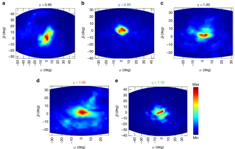
In order to understand the role of the extraction hole array on the far-field beam pattern, the intensity distribution of each device was sampled by scanning a pyroelectric detector in the plane orthogonal to the y–z surface at a distance of ~8 cm. As expected, the far-field intensity plots show different divergences
0 50 100 150 200 250
0.9 0.95 1
1.05 1.1
0 5 10 15 20
0 300 600 900 1200 1500 18000 10 20 30 40 50 60
Voltage (V)
Current density (A/cm2)
Peak optical power (mW)
d
P
/d
I
(mW A
–1)
=1.10
=1.05
=1.00
=0.95
=0.90
a
3.0 3.1 3.2 3.3 3.4 3.5 3.6 3.7 3.8 =1.05
=1.00
=0.95
Frequency (THz) c
b
900 1000 1100 1200 1300
10 50 90 130
d
Jth
(A cm
–2
)
Temperature (K)
Fig. 3Electrical and optical characterization.aVoltage–current density (V–J) and power–current density (L–J) characteristics measured at 20 K for a set of
devices with differentηvalues, in a nitrogen-purged atmosphere. All lasers are driven in pulsed mode with a pulse width of 200 ns and pulse repetition rate of 100 kHz. Optical power scales were corrected to account for the detector collection efficiency and the absorption of the polyethylene cryostat window. The device area is 0.074 mm2.bSlope efficiency measured at 20 K plotted as a function ofη, under the same experimental conditions shown ina, with
[image:5.595.134.459.50.323.2]as a function of the extraction wavevector (Fig.4a–e). For the case ofη=0.95, the beam is single-lobed and localized within a beam profile ofΔφ≈Δϑ≈10° (Fig.4b).
Such a divergence is expected to be reduced by the increase of the cavity length20,22, which can also have a beneficial effect on the optical power output22and slope efficiency.
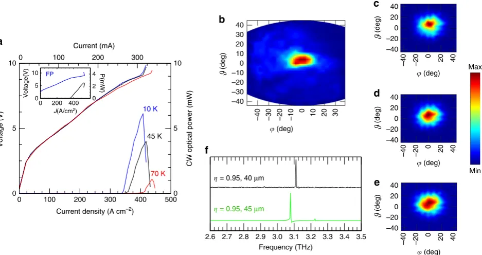
Our architecture also offers the potential for high power, low-divergent CW sources. In order to demonstrate this, a second set of resonators was fabricated on a different active region material31, designed to limit self-heating by Joule dissipation through having a lower operating current density and alignment bias. The resonator width was also varied in the 40–45 µm range to explore its effect on the resonant frequency and output power. Figure5a shows theV–Jand L–J characteristics of the device withη=0.95 and a width of ~45 µm, driven in CW at different operating temperatures. For comparison the inset of Fig.5a shows the CW performances of an edge-emitting FP THz QCLs, having comparable dimensions and fabricated from the same semicon-ductor heterostructure. A maximum CW optical power of 6 mW and a slope efficiency of 100 mW A−1 were measured in our
sinusoidal wire laser at a heat-sink temperature of 10 K, in a nitrogen-purged atmosphere, against the 2.5 mW of power achieved in the corresponding FP laser. The sinusoidal wire laser reaches maximum WPE in CW of about 0.23%, about 40% larger that that achieved in perfectly phase-matched third-order DFBs20. As shown in Fig. 5b, the far-field intensity pattern is characterized by a divergence ofΔφ≈8° andΔϑ≈12°, similar to the previous case. Numerical simulations of the far-field profile (Fig.5c–e) show that the diameter of the extraction hole array has a role in tailoring properly the optical beam shape: indeed by reducing the hole diameter by 50% (Fig. 5c) the beam shape divergence is slightly reduced in bothφandϑwith respect to the
selected 10 µm diameter holes array (Fig.5d); conversely a slight increase of the hole diameter (from 10 to 12 µm, Fig.5e) starts to significantly deteriorate the optical beam shape.
Figure5f shows the FTIR emission spectra for two devices with the same extraction parameter (η=0.95), but different sizes. The 40-µm-wide wire laser emits single mode at 3.11 THz, while the larger cavity (45 µm) emits a red-shifted peak at 3.08 THz and a less intense line at 3.22 THz. The spectral emission around 3.1 THz correlates well with the frequency of the lower-edge mode of the fundamental photonic bandgap, as computed in our 3D FEM simulations, which also predict a shift of≈25 GHz induced by the increased resonator size. In the case of the 45-µm-wide resonator, the low intensity high-frequency peak is very close to the computed frequency of 3.21 THz for the lower-edge mode of the second-order lateral bandgap. The variation of the average ridge width is also reflected in the maximum power output, which is ~10% lower for the 40-µm-wide device with respect to the 45-µm-wide structure. Since the mode has little overlap with the lateral pads and is mostly confined to the 1-mm-long sinusoidal mesa, the extracted optical power consequently scales with the width of the corrugated region. The ridge width also affects the beam collimation in the horizontal direction (φangle), since the 40-µm-wide device has a larger divergence of Δφ≈25°, while in the vertical direction, radiation has a divergence of Δϑ≈10°, comparable to that of the 45-µm-wide laser with same value of
η(=0.95).
Discussion
In conclusion, we have developed a new photonic wire THz resonator architecture exploiting a sinusoidal lateral ridge cor-rugation as the feedback grating, and a surface array of holes as
(deg) (deg)
Min Max = 1.10
40
30
20
10
0
–10
–20
–30
–40
–30
–40 –20 –10
0
10 20 30
= 1.05
30
20
10
–10
–20 0
–30 –20 –10 10 20
0
d e
(deg) (deg)
Fig. 4Far-field intensity patterns. Far-field emission patterns measured at 20 K while driving the devices in pulsed mode with 2% duty cycle, for wire lasers
[image:6.595.64.531.50.345.2]the extraction grating, the periodicity of which was tuned to optimize the extraction and enhance the output power and laser efficiency. A 42 mW of peak optical power was measured in pulsed regime, with a slope efficiency of ≈250 mW A−1. CW operation was also demonstrated with a maximum power output of 6 mW and a maximum WPE of 0.23%. The devices show good beam collimation with a divergence of ~10°. The reached power performances are due to the combined effect of the enhanced coupling losses of our proposed wire laser structure and to the significant beam reshaping which has a positive impact on the collection efficiency.
Optimization of the quantum design would enable the power efficiency to be increased significantly, with no deterioration in the threshold current density and with only a minor influence on the maximum operation temperature, constrained by the lossy absorbing boundary. Possible strategies to improve the present performances furthermore include: the reduction of the area of the lossy absorbing boundary pads to reduce the local lattice temperature, the increase of the wire laser length which plays an important role in increasing the output power and usually reducing the beam divergence20,22, the reduction of the thickness of the top highly doped contact layer underlying the un-patterned top metal surface to lower the waveguide losses, and increase the power extraction. Moreover, the use of broader gain region architectures would allow devising an array of on chip wire lasers for tuning the laser emission32; furthermore an on-chip mechanical architecture for continuous tuning can also allow adding a further functionality to the system. Remarkably, the proposed architecture is also easily scalable and does not have stringent lithographical constraints—very differently to other photonic engineering approaches reported to date. As such, our
devices could become an important underpinning platform for future applications in high-resolution spectroscopy, metrology, and quantum manipulation of cold atoms, for example.
Methods
Fabrication. Two different QCL heterostructures were used, both grown by
molecular beam epitaxy on an undoped GaAs substrate and consisting of a GaAs/ Al0.15Ga0.85As heterostructure. Thefirst structure (wafer L1023) is based on the
three-well resonant-phonon active region design reported in Reference29, with layer sequence:4.3/8.9/2.46/8.15/4.1/16 (in nm), where the Al0.15Ga0.85barrier
layers are indicated in bold, the GaAs wells are in roman, and the underlinedfigure indicates the presence of a 5-nm-thick Si-doped region in the center of thefinal well, with a Si doping concentration of 6 × 1016cm−3. The second structure (wafer V788) is described in ref.31and comprises a bound-to-continuum QCL with a
single-quantum-well phonon extraction stage. It features a layer sequence of5.5/ 11.0/1.8/11.5/3.8/9.4/4.2/18.4 (in nm), with the last well having a Si doping con-centration of 2 × 1016cm−3. After growth, a thermo-compressive wafer-bonding technique was performed, bonding the QCL onto an n+-GaAs carrier wafer with an Au–Au interface. After selective removal of the host GaAs substrate and an Al0.5Ga0.5As etch-stop layer, lateral absorbing pads werefirst defined through the
thermal deposition of a thin Cr layer (7 nm), to implement strong absorbing boundary conditions. Then, the sinusoidal top metallization with the extraction hole array was defined by ultra-violet photolithography and a subsequent Cr/Au (5 nm/150 nm) thermal evaporation, partly overlapping the Cr pads. The deposited metal acted as a mask during the inductively coupled plasma reactive ion etching (ICP-RIE) process, so that the n+top contact layer was selectively etched away only inside the extraction holes but not at the periphery, where the absorbing boundary provided by the Cr and the top contact layer is necessary. Finally, the laser cavity is defined by ICP-RIE etching of the wire laser, ensuring that the lateral corrugation is properly implemented through vertical etching of the semiconductor walls. As afinal step, the highly doped GaAs substrate was then lapped down to 150 µm. Individual devices were then indium soldered onto a copper mount and wire-bonded to both lateral pads to guarantee uniform current injection in the device. The FP edge-emitting QCL (from wafer V788) has been fabricated as follows: after a thermo-compressive Au–Au interface wafer-bonding technique of the QCL onto an n+-GaAs carrier the host GaAs substrate and the Al0.5Ga0.5As
0 5 10
0 100 200 300 400 500
0 100 200 300
0 5 10
Voltage (V)
Current density (A cm–2)
CW optical power (mW)
10 K
45 K
70 K Current (mA)
a
2.6 2.7 2.8 2.9 3.0 3.1 3.2 3.3 3.4 3.5 Frequency (THz)
= 0.95, 45 μm = 0.95, 40 μm f b c d e 4 2 0 400 200 0 10 5 0
J(A/cm2)
P(mW) Voltage(V) FP 40 40 20 0 –20 –40 –40 –20
0 20 40 Max Min 40 20 0 –20 –40 –40 –20 0 20 40 40 20 0 –20 –40 –40 –20 0 20 40 30 20 10 –10 –20 –30 –40
–40 –30 –20 –10 10 20 30
0 (deg) (deg) (deg) (deg) 0 (deg) (deg) (deg) (deg)
Fig. 5Continuous-wave operation.aVoltage–current density (V–J) and power–current density (L–J) characteristics measured in continuous-wave mode
[image:7.595.65.534.53.301.2]Measurement details. The spectra, light–current density (L–I) and current density–voltage (I–V) characteristics were measured in pulsed mode (typically 2% duty cycle, 200-ns-long pulses) for the devices fabricated from wafer L1023, and in CW for devices fabricated from wafer V194. The spectral characteristics were performed using a FTIR spectrometer, operating in rapid scan mode with a resolution of 0.125 cm−1and an internal deuterated triglycine sulfate (DTGS) detector. The emitted power was measured by a calibrated pyroelectric detector and by a Thomas Keating absolute THz power meter. The far-field emission patterns of the lasers were measured with a pyroelectric detector, having sensitive area of 7 mm2, which was scanned on a 8-cm-radius sphere centered on the device surface.
Theϑ=0,φ=0 angle corresponds to the direction parallel to the device surface.
Data availability. The authors declare that the data supporting thefindings of this
study are available within the paper or are available from the corresponding author upon request.
Received: 10 August 2017 Accepted: 14 February 2018
References
1. Eisele, M. et al. Ultrafast multi-terahertz nano-spectroscopy with sub-cycle temporal resolution.Nat. Photon.8, 841–845 (2014).
2. Tonouchi, M. Cutting-edge terahertz technology.Nat. Photon.1, 97–105 (2007).
3. Köhler, R. et al. Terahertz semiconductor-heterostructure laser.Nature417, 156–159 (2002).
4. Fasching, G., Benz, A. & Unterrainer, K. Terahertz microcavity quantum-cascade lasers.Appl. Phys. Lett.87, 211112 (2005).
5. Zhang, H., Dunbar, L. A., Scalari, G., Houdré, R. & Faist, J. Terahertz photonic crystal quantum cascade lasers.Opt. Express15, 16818–16827 (2007). 6. Chassagneux, Y. et al. Electrically pumped photonic-crystal terahertz lasers
controlled by boundary conditions.Nature457, 174–178 (2008).
7. Vitiello, M. S. et al. Photonic quasi-crystal terahertz lasers.Nat. Commun.5, 1–7 (2014).
8. Biasco, S., Li, L., Linfield, E. H., Davies, A. G. & Vitiello, M. S. Multimode, aperiodic terahertz surface-emitting laser resonators.Photonics3, 1–11 (2016). 9. Schönhuber, S. et al. Random lasers for broadband directional emission.
Optica3, 1035–1038 (2016).
10. Vitiello, M. S. & Tredicucci, A. Tunable emission in THz quantum cascade lasers.IEEE Trans. Terahertz. Sci. Technol.1, 76–84 (2011).
11. Wienold, M. et al. Lateral distributed-feedback gratings for single-mode, high-power terahertz quantum-cascade lasers.Opt. Express20, 11207–11217 (2012).
12. Kumar, S. et al. Surface-emitting distributed feedback terahertz quantum-cascade lasers in metal-metal waveguides.Opt. Express14, 113–128 (2007). 13. Amanti, M. I., Fischer, M., Scalari, G., Beck, M. & Faist, J. Low-divergence single-mode terahertz quantum cascade laser.Nat. Photon.3, 586–590 (2009). 14. Kogelnik, H. & Shank, C. V. Coupled-wave theory of distributed feedback
lasers.J. Appl. Phys.43, 2327 (1972).
15. Xu, G. et al. Efficient power extraction in surface-emitting semiconductor lasers using graded photonic heterostructures.Nat. Commun.3, 952 (2012). 16. Xu, G. et al. Surface-emitting terahertz quantum cascade lasers with
continuous-wave power in the tens of milliwatt range.Appl. Phys. Lett.104, 091112 (2014).
17. Mahler, L. et al. Quasi-periodic distributed feedback laser.Nat. Phot.4, 165–169 (2010).
in an ultra-narrow beam.Optica3, 734–740 (2016).
26. Vitiello, M. S. et al. Quantum-limited frequencyfluctuations in a terahertz laser.Nat. Photon6, 525–528 (2012).
27. Qiu, M. Effective index method for heterostructure-slab-waveguide-based two-dimensional photonic crystals.Appl. Phys. Lett.81, 1163–1165 (2002). 28. Yablonovitch, E. Inhibited spontaneous emission in solid-state physics and
electronics.Phys. Rev. Lett.58, 2059–2062 (1987).
29. Fathololoumi, S. et al. Terahertz quantum cascade lasers operating up to ~200 K with optimized oscillator strength and improved injection tunneling.Opt.
Express20, 3866 (2012).
30. Vitiello, M. S. et al. Thermal properties of THz quantum cascade lasers based on different optical waveguide configurations.Appl. Phys. Lett.89, 021111 (2006).
31. Amanti, M. I. et al. Bound-to-continuum terahertz quantum cascade laser with a single-quantum-well phonon extraction/injection stage.New. J. Phys.
11, 125022 (2009).
32. Castellano, F. et al. Tuning a microcavity-coupled terahertz laser.Appl. Phys.
Lett.107, 261108 (2016).
Acknowledgements
This work was partly supported by the European Union ERC Consolidator Grant SPRINT and by Regione Toscana through the FAR-FAS 2014 project DIAST and the FAR-FAS 2014 project SCIADRO (681379). A.G.D., E.H.L., and L.H.L. acknowledge support from the EPSRC (UK) (EP/J017671/1, EP/P021859/1), and from the Royal Society and Wolfson Foundation.
Author contributions
M.S.V. and F.C. devised the concept. S.B. performed the simulation. S.B and K.G. fab-ricated the devices and performed the experiments. L.L., E.H.L., A.G.D., H.E.B., and D.A. R. carried out the growth of QCL materials. M.S.V., S.B., and K.G. analyzed the data. M.S. V. and S.B. wrote the manuscript with the contributions from the other authors. M.S.V. coordinated the project.
Additional information
Competing interests:The authors declare no competing interests.
Reprints and permissioninformation is available online athttp://npg.nature.com/ reprintsandpermissions/
Publisher's note:Springer Nature remains neutral with regard to jurisdictional claims in published maps and institutional affiliations.
Open Access This article is licensed under a Creative Commons Attribution 4.0 International License, which permits use, sharing, adaptation, distribution and reproduction in any medium or format, as long as you give appropriate credit to the original author(s) and the source, provide a link to the Creative Commons license, and indicate if changes were made. The images or other third party material in this article are included in the article’s Creative Commons license, unless indicated otherwise in a credit line to the material. If material is not included in the article’s Creative Commons license and your intended use is not permitted by statutory regulation or exceeds the permitted use, you will need to obtain permission directly from the copyright holder. To view a copy of this license, visithttp://creativecommons.org/ licenses/by/4.0/.