Characterization of the blue emission of Tm/Er co-implanted GaN
I.S. Roqan1, C. Trager-Cowan1, B. Hourahine1, K. Lorenz2, E. Nogales1, K.P. O’Donnell1,
R.W. Martin1, E. Alves2, S. Ruffenach3, O. Briot3.
1 Dept. of Physics, University of Strathclyde, Glasgow G4 0NG, UK. 2 ITN, Estrada Nacional 10, 2686-953 Sacavém, Portugal.
3 Groupe d’Etude des Semiconducteurs, Université Montpellier II, 34095 Montpellier, France.
ABSTRACT
Comparative studies have been carried out on the cathodoluminescence (CL) and
photoluminescence (PL) properties of GaN implanted with Tm and GaN co-implanted with Tm and a low concentration of Er. Room temperature CL spectra were acquired in an electron probe microanalyser to investigate the rare earth emission. The room temperature CL intensity exhibits a strong dependence on the annealing temperature of the implanted samples. The results of CL temperature dependence are reported for blue emission (~ 477 nm) which is due to intra 4f -shell
electron transitions (1G
4→3H6) associated with Tm3+ ions. The 477 nm blue CL emission is
enhanced strongly as the annealing temperature increases up to 1200oC. Blue PL emission has also been observed from the sample annealed at 1200oC. To our knowledge, this is the first observation of blue PL emission from Tm implanted GaN samples. Intra-4f transitions from the 1
D2 level (~ 465 nm emission lines) of Tm3+ ions in GaN have been observed in GaN:Tm films
at temperatures between 20–200 K. We will discuss the temperature dependent Tm3+ emission in both GaN:Tm,Er and GaN:Tm samples.
INTRODUCTION
Extensive studies of GaN doped with rare earths (REs) (in-situ doped during growth or
implanted), have produced red, green and blue (RGB) emission from GaN:Eu, GaN:Er and GaN:Tm, respectively. The aim of these studies is to produce multiple color capability based on GaN:RE, for example, fabrication of white light LEDs through the light emission from co-doped GaN:Eu,Er,Tm. For example, Steckl et al (2001), have reported on multiple color capability
based on RE-doped GaN electroluminescence [1]. Intermediate colors from GaN:RE have been reported through MBE co-doping during growth, such as turquoise from GaN:Er,Tm and orange from GaN:Eu,Er [2]. The biggest challenge in the field of light emitting RE doped GaN is to obtain blue emission from GaN:Tm with high device efficiency. In this study, we present the RE luminescence properties of GaN co-implanted with Tm and a low concentration of Er.
REs in GaN replace gallium on a substitutional site of symmetry C3ν[3]. The 4f orbitals of RE
ions incorporated into semiconductors are so strongly screened that energy levels of the 4f
SAMPLES AND EXPERIMENTAL DETAILS
Tm and Er were co-implanted into undoped AlN-capped GaN epilayers which were grown by metal organic chemical vapour deposition (MOCVD) on c-plane sapphire. The GaN
and AlN cap are 2 µm and a few tens of nanometer thick, respectively [4]. Tm ions were implanted using a 300 keV ion beam. The SRIM simulations [5] predict that the ions stop at a depth of 54 nm underneath the AlN cap and 51 nm for uncapped samples. Whereas Rutherford Backscattering (RBS) depth-profiling shows the maximum ion concentration for uncapped material at a depth of ~70 nm and ~80 nm for capped materials, which is attributed to channeling effects [4]. The SRIM simulations and RBS show that Tm ions penetrate the AlN cap to stop in the GaN layer. Afterwards, samples were annealed for 20 min. at 1200°C (sample A), 1100°C (sample B), and 1000°C (sample C), at 3.8 bar pressure of N2gas. The samples were accidentally
co-doped with low fluence of Er (<< 1×10¹⁵ at/cm2). Reference sample D is Tm implanted into a 2 µm undoped MOCVD GaN epilayer grown on c-plane sapphire. No capping layer was present
for this sample. The implantation fluence was 3×10¹⁵ at/cm2. The sample was annealed under the same conditions as sample C.
CL measurements were carried out at room temperature, in a Cameca SX100 electron probe microanalyser. The spectra were acquired over a wavelength range of 430–830 nm with a spectral resolution of 1.2 nm. CL temperature dependent measurements were carried out in a home built CL spectroscopy system. The spectra were acquired over a wavelength range of 460– 490 nm with a spectral resolution of 0.05 nm, in the temperature range 20–300K. PL was excited using the 325 nm line of a He–Cd laser. PL spectra were acquired over a wavelength range of 460–490 nm in the temperature range 18–300 K with a spectral resolution of 0.4 nm.
EXPERIMENTAL RESULTS AND DISCUSSION
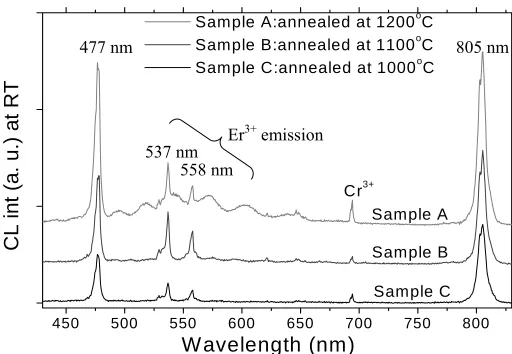
The CL spectra of GaN:Tm,Er and GaN:Tm recorded at room temperature (RT) are shown in figures (1) and (2), respectively. CL spectra of Tm/Er co-implanted GaN at different annealing temperatures include two major lines of the Tm3+ ion, in the blue at 477nm and near infrared (NIR) at 805 nm [6]. The green lines (537 and 558 nm) are related to intra – 4f inner
shell transitions of Er3+ ions [6].
As shown in figure (1) the RE3+ emissions are enhanced as the annealing temperature increases. A strong increase of CL intensity with annealing temperatures above 1000ºC has also been reported for Eu implanted GaN [4].
Our assignment for the RE3+ transitions is based on comparison with data from the literature [6-10]. The blue line at 477 nm and the near infrared line at 805 nm shown in figure (1) are attributed to the intra-4f transitions (1G4→3H6) and (3H4→3H6) of Tm3+ ions, respectively [6].
The two green lines at 537 nm and 558 nm are attributed to the intra-4f transitions (2H11/2→4I15/2)
and (4S3/2→4I15/2) of Er3+ ions, respectively [6]. The line at 694 nm, which appears in all spectra,
is the Cr3+ emission line originating from the sapphire substrate of the samples [6].
Figure (2) shows the CL spectrum of GaN implanted with a fluence 3×10¹⁵ Tm at/cm2 with a subsequent 1000oC anneal temperature (sample D). Comparing the spectra of Tm implanted with that of Tm/Er co-implanted GaN, we do not observe any significant differences in the Tm3+ emission lines. Comparing the spectra of Tm/Er implanted GaN (sample C) and Tm
477 nm to 805 nm peak intensities in GaN:Tm is ~0.4, whereas in GaN:Tm/Er (sample C) it is ~0.6. This ratio increases in the GaN:Tm,Er samples from ~ 0.6 (sample C) to ~1 (sample A) as the anneal temperature increases from 1000 to 1200°C, as shown in figure (1). Lorenz, et al,
observed a similar dependence on implantation temperature in Tm implanted GaN films [11]. For the sample annealed at 1200oC, a broad emission band emerges in the wavelength range 500–650 nm.
450 500 550 600 650 700 750 800
Sample C Sample B Sample A Cr3+
CL int (a. u.) at RT
W avelength (nm)
Sample A:annealed at 1200oC Sample B:annealed at 1100oC Sample C:annealed at 1000oC
Figure 1. Room temperature CL spectra of Tm/Er implanted GaN at different anneal
temperature, showing Tm3+ blue and NIR emissions at 477 and 805 nm and Er3+ green emission at 537 and 558 nm. The line marked Cr3+ originates in the sapphire substrate.
4 5 0 5 0 0 5 5 0 6 0 0 6 5 0 7 0 0 7 5 0 8 0 0
W a ve le n g th (n m ) C r3+ S a m p le D : (a n n e a le d a t 1 0 0 0oC )
CL
int.
(a.u.
) at
RT
Figure 2. Room temperature CL spectra of Tm implanted GaN, showing Tm3+ blue and NIR emissions at 477 and 805 nm.
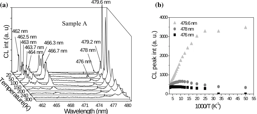
Figure (3a) shows high resolution CL spectra of the blue Tm3+ emission of sample A as a
function of temperature in the range 20–300 K. The Tm3+ CL spectra exhibit a number of different narrow lines in the blue region, particularly at low temperature. The different emission lines could possibly originate from different Tm3+ centres formed in GaN or be due to crystal field splitting of the Tm3+ levels [12-14].
The group of lines at 479.6 and 479.2, 478 and 476 nm is assigned to 1G4→3H6
transitions of Tm3+ [6-8]. The shorter wavelength group of lines (from 462 to 466.7 nm) can be attributed to 1D
2→3F4 transitions of Tm3+ [7, 8, 12]. As can be seen from the energy diagram,
477 nm 805 nm
537 nm Er
3+ emission
477 nm
805 nm
[image:3.595.162.418.196.373.2] [image:3.595.186.399.439.582.2]shown in figure (4), the 1D2 state is very close in energy to the band gap of GaN. The 1D2→3F4
transitions were not identified in GaN:Tm films in previous studies [6-10], although a strong emission has been observed due to transitions related to the 1D
2 level in GaN:Tm quantum dots
[8]. However, the final identification of these transitions requires further investigation.
Different peaks have different thermal quenching behavior as indicating in Figures. (3a) and (3b). The line due to the 1D2→3F4 transitions is completely quenched and vanishes at
temperatures above 200 K as shown in figure (3a). This may be due to the fact that the 1D2 level
is close to the band gap energy of GaN. Some of the lines related to the 1G4 level exhibit
intermediate behavior as shown in figure (3b). The emission line at 479.6 nm due to the transition from1G
4 decreases in intensity as the temperature increases, whereas the intensity of
the peak at 478 nm, which is related to the 1G4→3H6 transitions, grows continuously to reach its
maximum at 100 K. For temperatures up to 300 K, the decline of the 478 nm line is quite slow: at room temperature it is about 60% of its maximum at 100 K.
A new line peaking at 476 nm related to a 1G4 transition emerges when the temperature
reaches 40 K and grows slowly up to a temperature of 100 K. It saturates as the temperature increases up to 300 K. The nature of this line has yet to be determined. It may be related to thermal population of higher crystalline Stark split levels of 1G4, or Tm3+ centres of different
symmetry.
The emission lines at 478 and 476 nm, due to 1G4→3H6 transitions, show remarkably
small thermal quenching when compared to the emission of the 479.6 nm line (figure (3b)). The thermal quenching mechanisms are proposed to be mostly nonradiative recombination of the excited states of a localized RE3+ center in GaN [13]. These mechanisms could comprise multiphonon relaxation processes, and a migration of energy and cross-relaxation processes. If the energy gap to the next lower state is sufficiently large, the nonradiative multiphonon transition rate is negligible compared to the radiative rate [13]. This explains the weak temperature quenching of transitions of 1G
4 level and its strong CL emission at RT as shown in
figure (1).
462 465 468 471 474 477 480
CL int ( a . u ) 462 nm 462.5 nm 463 nm 463.7 nm 464 nm 466.3 nm 466.7 nm 476 nm 478 nm 479.2 nm 479.6 nm 300 240 200 150 100 50 20 Wavelength (nm) Tem pera tur e(K)
Figure 3. (a) Temperature dependence of CL spectra of GaN implanted with Tm and Er (annealed at 1200 oC). (b) The temperature dependence of CL peaks intensities related to
1G4→3H
6 transitions.
(a) (b)
Sample A
5 10 15 20 25 30 35 40 45 50 55 0 1000 2000 3000 4000 CL pe ak
int (a. u.)
1000/T (K-1)
[image:4.595.77.512.472.666.2]Figure 4. Free ion energy levels diagram of Tm3+ ions and assigned transitions of Tm implanted GaN. The band gap of GaN is also indicated in the figure, relative to the 3H6 ground state of the
free ion.
462 465 468 471 474 477 480 483 486 489 478 nm
478.2 nm 479.6 nm
at 30 K
PL
in
t.
(a
. u
.)
Wavelength (nm)
Figure 5. PL spectrum of Tm/Er implanted GaN and annealed at 1200oC in blue region. Tm3+ emission due to 1G4 →3H6 transitions is observed in PL. The emission due to 1D2→3F4
transitions has been not observed.
Figure (5) shows the PL spectrum of Tm3+ ions in GaN:Tm,Er (sample A) at low temperature. A weak luminescence was observed related to 1G
4→3H6 transitions. This is the first
observation of PL blue emission due to 1G
4→3H6 transitions from Tm implanted GaN to our
knowledge. The transitions originating on the 1D2 level are not seen. This illustrates the
complexity of the energy transfer when comparing PL and CL. Future study of selective excitation and time-resolved temperature dependence should clarify our tentative assignments and the energy transfer process.
To investigate the effect of the presence of Er3+ ions on Tm3+ emission, we studied the thermal quenching of Tm (only) implanted GaN which has the same implantation and annealing conditions as (sample C) GaN:Tm,Er. From the CL spectra studies of Tm3+ emission in GaN:Tm
[image:5.595.204.389.105.259.2] [image:5.595.182.406.334.465.2]CONCLUSIONS
We have carried out preliminary studies of the PL and CL emission and thermal
quenching of Tm3+ in the presence of a low concentration of Er3+ ions. We found that the ratio of Tm3+blue emission to NIR increased as the anneal temperature increased. From our studies we show that the energy transfer to 1D2 level in blue region of Tm3+ ion is allowed in GaN:Tm,Er
and GaN:Tm films. Blue PL Tm3+emission has been observed from implanted GaN films for first time to our knowledge. We compared the luminescence properties of Tm/Er co-implanted GaN with Tm implanted GaN to investigate the effect of the presence of Er3+ ions on Tm3+ emission. We found that co-implanted with low concentration Er did not have a detrimental effect on the Tm luminescence temperature dependence.
REFERENCES
[1] A. J. Steckl, J. Heikenfeld, D. S. Lee and M. Garter, Mat. Sci. Eng. B 81, 97 (2001). [2] A. J. Steckl and J. M. Zavada, MRS Bull. 24, 33 (1999).
[3] H. J. Lozykowski W. M. Jadwisienczak and I Brown, J. App. Phys. 88, 210 (2000).
[4] K Lorenz, U. Wahl, E. Alves, S. Dalmasso, R. W. Martin, K. P. O’Donnell, S. Ruffenach and O. Briot. Appl. Phys. Lett. 85, 2712 (2004).
[5] J. F. Ziegler, J. P. Biersack, U. Littmark, The stopping and range of ions in solids (Pergamon Press, New York, 1985).
[6] H. J. Lozykowski W. M. Jadwisienczak and I Brown, Appl. Phys. Lett. 74, 1129 (1999). [7] U. Hommerich, Ei Ei Nyein, D. S. Lee, A. J. Steckl and J. M. Zavada, Appl. Phys. Lett. 83, 4556 (2003).
[8] T. Andreev, Y. Hori, X. Biquard, E. Monroy, D. Jalabert, A. Farchi, M. Tanaka, O. Oda, Le Si Dang, and B. Daudin, Phys. Rev. B 71, 115310 (2005).
[9] U. Hömmerich, Ei Ei Nyein, D. S. Lee, J. Heikenfeld, A. J. Steckl and J. M. Zavada, Mater. Sci. Eng. B 105, 91 (2003).
[10] D. S. Lee and A. J. Steckl, Appl. Phys. Lett. 83 2094 (2003).
[11] K. Lorenz, U. Wahl, E. Alves, S. Dalmasso, R.W. Martin, K.P. O`Donnell, MRS Symp. Proc. 798, Y5.4 (2004).
[12] M. D. Seltzer, J. B. Gruber and M. E. Hills, J. Appl. Phys. 74, 2821 (1993). [13] H. J. Lozykowski, Phys. Rev. B 48, 17758 (1993).