Rochester Institute of Technology
RIT Scholar Works
Theses
Thesis/Dissertation Collections
2-1-1997
A Morphological array image processor controller
chip set
Christopher Insalaco
Follow this and additional works at:
http://scholarworks.rit.edu/theses
This Thesis is brought to you for free and open access by the Thesis/Dissertation Collections at RIT Scholar Works. It has been accepted for inclusion in Theses by an authorized administrator of RIT Scholar Works. For more information, please [email protected].
Recommended Citation
A MORPHOLOGICAL ARRAY IMAGE
PROCESSOR CONTROLLER CHIP SET
by
Christopher
J.
Insalaco
A thesis submitted
Inpartial fulfillment of the
requirements for the degree of
Master of Science
InComputer Engineering
Approved by: Prof.
_
George A. Brown, Thesis Advisor
Prof.
_
Robert E. Pearson
Prof.
_
Roy S. Czernikowski, Department Head
Department of Computer Engineering
College of Engineering
Rochester Institute of Technology
Rochester, N ew York
A MORPHOLOGICAL ARRAY
IMAGE PROCESSOR
CONTROLLER CHIP SET
I Christopher
J.
Insalaco hereby
grant permission
to the Wallace Library of
the Rochester Institute of Technology to reproduce my thesis
in
whole or
in
part. Any reproduction
will not be for commercial use or profit.
RochesterInstituteof
Technology
Abstract
AMORPHOLOGICALARRAY IMAGEPROCESSOR CONTROLLERCHIP SET
by
ChristopherJ. InsalacoThe
design,
simulation andlayout of a controller chip set for a morphologicalarray image processor shall be discussed. These VLSI chips in conjunction with the Morphological
Array
Processor(MAP)
and Arithmetic Logic Unit(ALU)
chip sets perform the morphological imageprocessing
operations of erosion and dilation on 512x512 pixel, 8-bit gray scale images using a 7x7 windowingmatrixinrealtime (60 framesper second). The controllerchip set design allows for pipelining of successive MAP's as well as operation on 1024x1024 pixel,8-bit grayscaleimages.To facilitate the
design,
additional scaleable CMOS standardlibrary
cells and correspondingparameterizedschematiclibrary
components were designedand integrated with the RIT CMOS standard celllibrary
designedby
ComputerEngineering
graduate studentLarry
Rubin as part of his Masters thesis1. In particular, additional D flip-flops with bothQ
andQ
bar outputs,and-or-inverts,
or-and-inverts,CMUXes,
and MOSIS 64 and 84 pin pad rings were created. The cells were designed to be fabricated using the Metal Oxide Semiconductor Implementation System(MOSIS)
scaleable CMOS 2.0 pmchips were designedand sent to MOSIS for fabrication. The layoutanddesign rule verification of the final two test chips, test chips five and six, was
performed
by
the author. Test chip four contains avariety ofMUXes and Dflip-flops,
testchip five containsavarietyoftransfergates andinverters.Thecontroller chipsetconsists ofa64pincontrolchip
(Controller)
and an 84pin
memory
controller chip (Mem_Control). The controller chips provide theability to selectively process 512x512 or 1024x1024 image sizes
by
modifying thepullup
or pulldown of a "size" bit. A selectabledelay
wasimplemented,
through thepullup or pulldownsetup ofthree
delay
bits,
inthe ControllertoTABLE OF CONTENTS
ABSTRACT iii
LIST OF FIGURES vii
LIST OF TABLES ix
L INTRODUCTION 1
EL HISTORICALREVIEW 2
A. Design BeforetheLibrary 2
B. Test Chips 3
C. The Commissionof aMorphological Chip Set 5
DI.THEORY 7
A. Morphology 7
1.EUCLIDEAN MORPHOLOGY 8
2. DIGITAL MORPHOLOGY. 12
3. GRAY SCALEMORPHOLOGY 14
B. Design RuleChecking 16
IV. MATERIALSANDAPPARATUS 23
A. MentorandCadence Tools 23
B. Tektrontx Logic Verifier 27
V. METHODOF PROCEDURE 27
A.Cadence DraculaHLayout Verification Tools Setup 29
B. Additional Standard Cells 31
C Test Chips 5and6 37
D. Morphological Array Processor Controller Design 40
1. The Functional Design ArchitectureoftheMAPController
Chip
40 2. TheTop
LevelDesignoftheMAP ControllerChip
Set 66 3. The Logic Design oftheControllerandMemjOontrol 75 4. The Logic SimulationoftheControllerandMemControl. 91 5. TheCircuit DesignoftheControllerandMemControl 93 6. TheCircuit Simulation oftheControllerandMemControl 93 7. TheMorphologicalArray
ProcessorTop
Level Simulation 948. The LayoutoftheControllerandMemControl 95 9. Suggested
Testing Methodology
fortheControllerandMemControl 98VL RESULTS 98
VHLCONCLUSIONS 102
A. Future Work 103
APPENDIX A 105
DRC.COM File 105
APPENDIXB 109
LVS.COM File 109
APPENDIXC Ill
LPE.COMFile Ill
APPENDIXD 114
Simulation Files 114
1. Start Blank Physical Simulation File 114 2.Start BlankPhysicalSimulation Results 117
3. Start BlankLogical Simulation File 118
4. StartBlankLogical Simulation Results 120
APPENDIXE 121
Layout Plots 121
REFERENCES 125
LIST OF FIGURES
Number Page
Figure1 SpacingCheck 19
Figure 2 Enclosure Check. 19
Figure 3 Transistor Overlap Check 20
Figure4Transistor Spacing Check 20
Figure5CMUX4 Schematic 32
Figure6 DLAT Schematic 33
Figure7 DLATAR Schematic 34
Figure 8 ND3_2 Schematic 35
Figure9 NR3_2 Schematic 36
Figure 10 Test_Chip_5 Schematic 38
Figure 11 Test_Chip_6 Schematic 39
Figure 12 ImageandWindow Matrices 43
Figure 13 Morphological Array Processor Architecture 44
Figure 14 Blanking Bits 48
Figure 15 Blankingpart 1 53
Figure 16 Blankingpart2 54
Figure 17 Blankingpart 3 55
Figure18Blankingpart4 56
Figure 19 Blankingpart5 57
Figure 20 Blankingpart6 58
Figure21 Blankingpart7 59
Figure 22 Blankingpart 8 60
Figure 23 Blankingpart9 61
Figure24Blankingpart10 62
Figure 25 Blankingpart11 63
Figure 26 Blankingpart12 64
Figure 27 Image_Processor Schematic 67
Figure28Controller_ChtpSchematic 79
Figure29 Controller Schematic 80
Figure30 VarJDelay Schematic 81
Figure3 1 Bus_Select Schematic 82
Figure 32 Mem_Select Schematic 83
Figure 33 StartBlankSchematic 84
Figure 34 BlankCounter Schematic 85
Figure35Mem_Control_ChipSchematic 86
Figure36Mem_Control2Schematic 87
Figure37Mem_ControlSchematic 88
Figure3 8 Mem_Counter Schematic 89
Figure 39 MUX2xl0 Schematic 90
Figure40 ControlTimingDiagram 92
Figure41 PowerRouting Architecture 97
Figure43Start_BlankLogical Simulation Output 120
Figure 44 SCCCB Layout 121
Figure 45 SCCCBA Layout 122
Figure 46 SCCCBNA Layout 123
LIST OF TABLES
Number Page
Table1Binary Plxel ValuesandTheir Decimal Equivalents 41 Table 2 Blanking Control Values For All Index Values 48
Table 3 Blanking Control Values 50
Table4Blanking Control Values
(cont'd)
51Table 5 Controller Inputs / Outputs 69
Table 6 MemControl Inputs / Outputs 73
Table 7 WriteEnable Truth Table 77
ACKNOWLEDGMENTS
To Lindaand
Michelle,
whomakeitallworthwhile.Theauthorwishesto thankJeffCorrell forhis
help
withthecelllibrary
andtheincorporationoftheREMEDIdesignrule checkerinto theChipgraphmacros,
Shishir Ghate for his
help
with the celllibrary
and ALU design and theintegration of the
library
withCellstation,
Jeff Hanzlik for hishelp
with thelogical definition of the
MAP,
JensRodenberg
for the MAP Architecturesection andthelogical design ofthe
Controller,
andLarry
Rubin for his workin
designing
the celllibrary,
enhancing the design automation tools and the
LIST OF ABBREVIATIONS
ALU
Arithmetic
Logic UnitCAD
Computer Aided DesignCIF Caltech IntermediateForm
CPF
Circuit Path FinderDRC
Design Rule CheckerERC Electrical Rule Checker
HDL Hardware Description Language
IBM International Business MachinesInc.
LPE Layout Parameter Extractor
LVS Layout Versus Schematic
LSI Large Scale Integration
MAP Morphological
Array
ProcessorMOSIS MetalOxide Semiconductor Implementation System
MSI Medium ScaleIntegration
NSA National
Security
Agency
RIT Rochester Institute of
Technology
SSI Small Scale Integration
Accusim, Cellgraph, Chipgraph, Expand,
Extract,
IDEAStation, MCIF,
Mspice, Neted, REMEDI,
and Symed are registered trademarks of MentorGraphics Corporation.
Dracula II isaregisteredtrademarkofCadenceInc.
I. Introduction
To verifythedesignoftheRIT CMOSstandardcell
library,
created as apartofLarry
Rubin'sthesis1,
it became necessaryto setup layoutverificationtools forthe MOSIS 2pmN-wellCMOS process. Itwas decidedthat theMOSIS dense
rule set wouldbeusedtoallowformorecompacteddesign layouts.
So,
a set ofrules checkers to automate the design verification for this process became
necessary. The Cadence Dracula II tool set will be used in this work;
specifically the Cadence design rule checker
(DRC),
electrical rule checker(ERC),
layout versus schematic(LVS),
and layout parameter extractor(LPE)
products. A
technology
(".com")
file must be defined for the MOSIS dense rule set foreachoftheproductsintheCadencetoolset.Additional RIT CMOS standard cellswillbe
designed,
layedout,and verified asnecessaryto complete the morphologicalarray controller chip set. Inaddition
test chips willbe layed out andsent to MOSIS for fabricationto test some of
thestandard celldesigns.
Once the verification tools and additional RIT CMOS standard cells were
defined,
they
were utilized to create amorphological array controller chip set for use with the morphological array processor(MAP)
chip set designedby
Larry
Rubin,
and the pre andpost ALU chip set designedby
Shishir Ghate2. Thefollowing
arethedesigngoals forthecontrollerchip set:1. tomatchthe
functionality
oftheACTELcontrollercircuitry design ofJens Rodenberg33. toworkinconjunctionwiththe
timing
andcontrol signals oftheMAPandALU
chip sets to allowthe morphologicalimage processing operations of erosion and dilation on 512x512 or 1024x1024 pixel nine-bit gray scaleimageswith a7x7window
4. toallowfuture designs usingthe controller andMAPtobepipelined
5. toallowfuture designsto havemorethanfour
memory
units6. to fit the controller chip set onto MOSIS standard 64and 84pin padring chips
II. Historical Review
A.
Design BeforetheLibrary
Without the RIT CMOS standard cell
library
a designer would have had to enter two different sets of schematics to do both logical and circuit level simulations. This is both inefficient andunreliable, as there is no mechanism toverifythelogic levelschematic withtheequivalenttransistorlevelschematic.Another drawback of the generic logic level
library (gen_lib)
suppliedby
Mentor
Graphics,
is that every component has a defaultdelay
ofzero when simulated. This is overly optimistic, and prevents operation in systems withfeedback,
such as an SR latch. Race conditions are not modeled, nor aresettlingglitches ofthe circuit's outputs. The
library
solves these problemsby
Before the
library
was created, no standardized mechanism existed to actuallyfabricate designs throughtheMOSISprogram.The SPICE fileswere obsolete,
and overly simplified
(they
did not model leakage current or junctioncapacitance) andtherewere nopadcells.
For the design and implementation of any VLSI project, especially if it is
intended to be
fabricated,
the compilation of a standardlibrary
is not onlypractical, but a necessary and an inevitable evolutionary stage of any CAD
center.
B.
Test
ChipsAt the time the RIT cell
library
was proposed, MOSIS supported twelvedifferentprocesses,
including
2.0,
1.6,
and 1.2micron CMOS and even aGaAs process. A standard ceElibrary
(withno components) available fromMOSIS,
was developed at the
University
of Mississippi for the NationalSecurity
Agency. This cell
library
is publicly available. When the RIT celllibrary
wasproposed,
Larry
Rubin designed and fabricated a test chip to compare someprototype cells with the equivalent cells supplied
by
the NSA to determine iftherewereany advantages togenerating a complete
library
from scratch1. Thealternative would have been to create a matching component
library
for theNSA celllibrary.
The test chip consisted of
MUXes,
Dflip-flops,
and an 8-bit adder. TheMUXes compared the RIT nMOS and CMOS transmission gate MUXes
against the NSA MUX called "dsel". A D
flip-flop
with asynchronous resetsfrom each
library
was used. For overall speed comparison, two 41-stagering
The RITcellsrequired 1/3to 1/2theareaoftheequivalentNSA cells,andhad
less input capacitance,while
having
the same drive capabilities. Because ofthis,the RIT cells were faster. Due to less than maximal contacting and
unnecessarilythinpowerrouting inthe NSA cells
(causing
unnecessary internalresistance),theRITcells were calculatedto consumelesspower.
Anotheradvantage oftheRITceEsis thatthereare severaldrivesizes available
for each component. The
inverter,
for example, has nine different drive sizesforthedesignerto choose from. The NSA
library
offers two sizes ofinverter,
and only one drive size was available for most ofthe cells. After all of theseconsiderations were taken into account, it was obvious that a more useful
library
wouldresultby
developing
it fromscratch.The testchip hasthe distinction of
being
the first RIT design tobe processed atMOSIS.To testthe
functionality
ofthecelllibrary,
5additionaltestchipswere designed and fabricatedby
Shishir Ghate2. Each component on the test chips has itsown output pad. This was done to allow for more accurate results from the testing. One could have conceivably placed many more components inside
each test chip and multiplexed the outputs. Although this would have allowed more components to be tested per chip, it was determined that the
multiplexing would have been detrimental to the final cause of obtaining accurateresults.
C. The Commission
of aMorphologicalChip
Set
In April
1990,
Professor EdwardDougherty
from the Center forImaging
Science discussed morphologyandthemorphologic operations of erosions and
dilationswiththe
faculty
inthe ComputerEngineering
Department.In June
1990,
ComputerEngineering
graduate student Jeff Hanzlik wasselected as principal investigator for the exploration of a prototype
morphologic platform. Itwas decidedtoimplementa 7x7 morphologicalarray
processor on a printed circuit board that could be inserted into an IBM
PC/AT compatible machine and operate on 512x512 pixel 8-bit gray scale
images4.
In September of
1990,
ComputerEngineering
graduate student JensRodenberg
joined the project.Initially
working with simulations ofmorphological operations he developed a new architecture
by
November,
wherebythe undefinedpixels (represented mathematically
by
negativeinfinity)
were
implicitly
definedvia controlbits,
as opposed to the original architecturethat required explicit negativeinfinities in the data path. The new architecture
also employed enhanced pipelining,
thereby
increasing
the efficiency of theprocessor3.
An initialgoal wasto fittheprototype onto anATstandard cardusing ACTEL
gatearraychips.Thisprovedtobe
impossible,
astheActelgatearraychipsthatwereuseddidnotallow ahighenoughlevelofintegration. Itwas also originally
desired to have the prototype operate in real time.
Again,
due to Actel speedlimitations,
thetechnology
prevented the desired performance frombeing
In 1991 Computer
Engineering
graduate student Lawrence Rubin joined theproject with the goal of
designing
a single VLSI chip MorphologicalArray
Processorthatwouldreplace 23 oftheActelgate arrays fortheprocessorarray
itself1.
Later,
ComputerEngineering
graduate student Chris Insalaco joined theproject to design a smaller more integrated
2-chip
set Controller to replace 5Actelgate arrays ofthe control
logic,
while alsoincreasing
performance. AlsoComputer
Engineering
graduate student Shishir Gate joined the project todesign the pre and post Arithmetic Logic Units for the MAP chip set to
III.
Theory
A.
Morphology
Morphological image
processing
refers to the analysis andprocessing
of animage based upon a knowledge of its structure or form with the intent of
modifying
that form or structure. The theoretical basis for morphologicalimage
processing
dates back to the work of H. Minkowski on spatial setalgebra. Based upon this work, G. Matheron and J. Serra of France and S.
Sternberg
of the U.S. have developed a set-theoretic approach to imageprocessing5'6. In this approach,
binary
images are treated as sets in abackground space that can then be actedupon
by
the usual set operations ofunion and
intersection,
in conjunction with another image set called astructuring element. The structuringelement is used to probe or fit the image toextractinformationaboutits shape.
For grayscale images theset operations of union andintersection become the
maximum andtheminimum
functions,
respectively.The two fundamental morphological operations are dilation and erosion. Dilation of an image yields an image that is uniformly larger than the original
image while erosion of an image yields a uniformly smaller image.
Building
upon the basic morphological operations, a large variety of morphological
filters can begenerated for such applications as edge
detection,
segmentation,/.
EUCLIDEAN MORPHOLOGY
Morphological operations are built upon the set operations union and
intersection
as well as the translationand reflectionoperations. GivenanimageA inR2
thetranslationofA
by
thepointxin R2is defined by:
T^A =
{a
+x : a eA}
wheretheplussignreferstovector addition.(1)
Considering
the pointx to be avectorin the plane, T^A. is A translated alongthe vector x. A reflected
image,
B^ in R2 is one that has been rotated 180around the origin or alternatively one that has been flipped from left to right
and
from
top
to bottom. The first fundamental operation in morphologicalanalysis is Minkowski addition. Given two images A and B in R2 , the
Minkowskisumis definedas:
AB =uTbA = u
{a
+b:aeA}
(2)
beB beB
A Bisconstructed
by
translating
Aby
each element ofBandthentaking
theunion of all the resulting translates. The second fundamental morphological
operation is Minkowski subtraction. Given two images A and B in
R2,
Minkowskisubtractionis definedas:
A0B = nTbA = n
{a
+b:aeA}
(3)
beB bB
A B is constructed
by
translating
Aby
every element of B then theintersection oftheresultingtranslatesistaken.
In morphological processing, the Minkowski sum is referred to as a
dilation,
D
(A,B)
= A B(4)
The morphological operation erosion has two different definitions in the
literature. Serra defineserosionasMinkowskisubtraction6,denotedas:
E
(A,B)
=A 0 B(5)
whereas
Sternberg
andMatheron6defineerosionas:E
(A,B)
=A 0B^ = nTJl(6)
beBAThis seconddefinitionoferosion willbe usedforourpurposes asit lendsitself
betterto a digital implementation. Thesecondimage B is generally referredto
as the structuring element. If B =
BA,
as it usuallydoes,
then erosion againbecomes equal to Minkowski subtraction. Another form of the Minkowski
subtraction equation is very useful in image processing, it states that the Minkowski subtraction ofB from A is composedofall elements x in
R2
such
thatBtranslated
by
xisasubset ofA,
whereB^0. This is denotedas:A B = {x:T^Ac
A}
(7)
Thisequation can alsobewritten as:
AOB^^iT^cA}
(8)
Analternativedefinitionof erosion canthenbewritten as:
Another form ofthe Minkowskiaddition
(dilation)
is also veryuseful Itstatesthat the Minkowski sum is composed of all elements x in R2
such that BA
translated
by
xisnota subset ofA,
whereB^0.
Thisis denotedas:D(A^)
={x:TIBA(rA}
(10)
These are the forms ofthe erosionanddilation equations that are usedin the
digital implementation.
Erosion anddilation areoftenperformedin succession onanimage.A dilation
followed
by
an erosionis calleda "closing" operationandis denoted:C
(AJ3)
= E(
D(AJT),
B*)
= (A9BA)0B (11)
An erosion followed
by
adilationis calledan "open" operationandis denotedby:
O
(AJ3)
=D(
E(A3),
B)
= (ABA)
B(12)
Some of the properties of Minkowski addition, Minkowski subtraction,
openingandclosingwill nowbepresented.
A B =B A additioniscommutative
(13)
A B*B A subtractionisnotcommutative
(14)
(AB)C=A(BC)
additionisassociative(15)
Associative addition allows structuring elements to be decomposed and
chained to achieve the effect of larger structuring elements from small
(AB)C
=Ac0B
(16)
(A
0
B)c=Ac B
(17)
Dilation and erosion are dual properties, the dilation ofthe background of an
objectisthe sameasthe erosion oftheobject,and vice versa.
ifAcBthenABcBC
(18)
ifAcBthenA0BcB0C
(19)
Additionand subtractionare both
increasing
operations.A(TJB)=TX(AB)
(20)
A<8>
(T3)
=CTA)
0 B =TX(AB)
(21)
Additionandsubtractionarebothtranslationinvariant.
O
(A3)
cA(22)
Open is antiextensive, the open operationtends to decrease the spatial extent
ofanimage.
C
(A3)
2A(23)
Closeis extensive,theclose operationtends toincreasethespatialextent ofan
image.
O (O
(A,B),
B)
= O(A,B)
(24)
C (C
(A,B),
B)
= COpenand close areidempotent (repeatedapplicationshaveno effect).
if A cFthenO
(A3)
c O(F,B)
(26)
ifA cFthenC
(A3)
cC(F,B)
(27)
Openandcloseare
increasing
operations.2.
DIGITAL MORPHOLOGY
Let F
(j,k)
be abinary
valued image matrix. A pixel at coordinate(j,k)
is anelement ofimage F
(j,k)
ifand only if it is a logical one. An image B(j,k)
is asubset ofan image A
(j,k)
if for every logical one pixel in B(j,k)
there is alogicalonepixelin A (j,k). An image Fc
(j,k)
is the complement ofF(j,k)
ifallthe pixels in Fc
(j,k)
are the oppositelogically
of those in F (j,k). A reflectedimage FA
(j,k)
is formedby
flipping
theimagematrix F(j,k)
from left to rightandfrom
top
to bottom. Translation of animage consists ofshiftingtheimageby
rrows andc columnsfromtheorigin.Thisis denotedas:G(j,k)
=TI>c{F(j,k)}
(28)
For the
following
definitions,
assume anNxNimage matrixF(j,k)
and anLxL,
where L is odd, structuring element matrix H (j,k). Minkowski addition is
defined,
similarto the Euclideancase,as:G
(j,k)
=UTr,c
{F
QJl)}
(29)
The
resulting image
size is MxM where M = N + L 1. The definition ofdilationisthen:
G(j,k)
=F(j,k)H(j,k)
(30)
Minkowskisubtractionis similarly definedas:
G(j,k)
=nTr>c{F(j,k)}
(31)
(r,c)eH
andthedefinition oferosionisthen:
G
(j,k)
=FG,k)
0HA(j,k)
= nT,,c
{F
(j,k)}
(32)
(r,c)eH-Another definition of
dilation,
analogous to the alternate definition in theEuclideanmodel, based on the scanning and
processing
ofH(j,k)
over F(j,k)
is:
G
(j,k)
= U{F
(m,n)
nH(j-m+S,
k-n+S)}
(33)
(m,n)
where max[l,
j-Q]
< m <minfN,j+Q]
and max[l,k-Q]
< n < min[N,k+Q]
andS = (L+ l)/2and
Q
= (L- l)/2.Thealternate definition forerosionis similarly definedas:
G
Q,k)
= n{F
(m,n)
U H(j-m+S,
k-n+S)}
(34)
(m,n)
where the same limits apply as for dilation. The digital opening and closing
equations can also be defined analogously to the
corresponding
Euclideanoperatorsas:
O (F
Ji)
=D(
E(F,H),
H)
= [F(j,k)
0
HAC
(F.H)
= E(
D(F,*r), H")
= \F(j
,k) HA(j
*)]
H(j,k)
(36)
3.GRAY SCALE
MORPHOLOGY
Let F
(j,k)
beagrayscaleimagequantized to anarbitrarynumber ofgraylevels,
n, whose pixelvalues can be between zero and 2n
- 1 or
undefined, (*).
Only
definedpixelsmay beelements ofthegrayscaleimage.Anundefinedpixel
may
come about
by
avarietyofmethods. It may be dueto a sensorproblemorthepixelmay simply be outofthebounds oftheimage. For gray scaleimages the
union operationis interpreted as the maximum ofthe two inputimages taken
point
by
point. The intersection operation is interpreted as the minimum ofthe two images taken point
by
point. The usual maximum and minimumdefinitions canbe extendedto include undefinedpixelvalues
by
treating
(*)
asif it were negative infinity. The max oftwo defined pixels is the highest value
pixel themax of a defined and an undefined pixel is the defined pixel value,
the max oftwo undefined pixels is (*). The min oftwo defined pixels is the
lowestpixelvalue, the min of a defined and an undefinedpixelis
(*),
and themin of two undefined pixels is (*). The complement Fc
Q,k)
of a gray scaleimage F
(j,k)
is foundby
replacing every pixel value,i,
with 2" 1 - i. Thetranslation, and reflection ofa gray scale image are defined and denoted the
same as
they
are for abinary
image. For an NxN image matrix F(j,k)
and anLxL,
where L is odd, structuringelement matrix H(jjs),
gray scale Minkowskiadditionis defined as:
G
(j,k)
=max[Tv
{F
(j,k)}]
(37)
(r,c)eH
G(j,k)
=min|Tr>c{FO,k)}]
(38)
(f,c)
eHThealternate formofthedilationoperationis definedas:
G
(j,k)
= max [F(m,n)
+H(j-m+S,
k-n+S)]
(39)
The alternateform oftheerosionoperationis definedas:
G
(j,k)
=min \F
(pap)
+H(j-m+S,
k-n+S)]
(40)
wherethe samelimits asabovefor
binary
images hold. Itmay beofinterest tocomparethe above equation withthe
defining
equationforconvolution. Inthedilation and erosion equations themaxor minoperations are analogous to the
summations in the convolution equation andthe point
by
point additions areanalogous to the point
by
point multiplication's in the convolution equation.Similar to convolution, dilation can be thought of as the scanning and
processing ofF
(j,k) by
H(j,k)
rotatedby
180 . The gray scaleopening and
closingoperations are onceagaindefinedas:
O
(F,H)
= D(
E(F,H),
H)
= [F(j,k)
HA(j,k)]
H(j,k)
(41)
C
(F,H)
=E(
D(F,HA),
HA)
= \FG,k)
HAQ,k)]
0 HQ,k)
(42)
where nowgray scale erosions and dilations are performed. Because the max
and min operations involved in erosion and dilation can be performed
sequentially, the erosion and dilation operations can be decomposed into a
series ofiterative erosions ordilations toaccomplishthesame effect as alarger
structuring element. Three iterations of a morphological image
processing
operationusing a 3x3 structuringelement accomplishes thesame effect as one
B. Design Rule
Checking
A design rule checker checks that the widths, spacings, and overlaps ofthe
features in a layoutmeet some minimum rules, the designrules. These design
rules are due to the limitations inthe integrated circuitmanufacturing process.
Many
differentmechanisms can contribute todeviations in feature shapes suchas electromigration, maskmisalignment, overetching, variations in photoresist
exposure, and the spread ofdiffusion and implant regions around transistors.
The purpose of design rules is to attempt to guarantee that, under the
accumulated set of process variations, the circuit continues to function as
designed. The Mead and
Conway
design rules are specified in relative termsusinga scaleable unit,lambda
(X),
instead ofdistances such as microns7.Thesedesignrules are conservative enoughto allow fabricationat a smallergeometry
by
simply changingthevalueofX.Using
themostconservative value for eachdesign rule, a simple set of spacing rules is produced. If layout
density
isimportant,
then a larger variety ofdesign rules must be considered. There is atrade-offofincreased design checking time for denser rule sets because more
complicateddesignrulesinvolvemorechecks.
Design rules are constraints imposed on the geometry oflayouts expressed as
minimum separations andminimum sizes oflayout features. Designchecksare
specified between both drawn layers and derived
layers,
that is layers that aremade up of combinations of the drawn layers. For example, transistors are
created at the areas where polysilicon and diffusion overlap. The analysis
software canperform the Boolean operations
AND, OR,
and NOT on theselayers to create derived
layers,
such as a transistor layer. The more derivedlayers
that aredefined,
the greater the design checking time and memoryutilization.
Integrated circuit layouts consist ofa collection ofpolygons of various colors
representing
features in different mask levels. Design rules generally specify rules onthe edges ofthepolygons,insteadof onthepolygons themselves. Onemethod ofrule checking is to breakpolygons and rectangles down into their
edges and perform rule checking on the edges. This
initially
increases theamountofdataobjects as therearemore edgesthanpolygons.
But,
itturnsout that half ofthe edges can be removed from the edges data without loss of informationby
addinga direction bit to indicatewhich side ofthe edgeis the insidearea. Because almost all layouts are orthogonal, usually halfoftheedgescanbe eliminated.
Other methods of design checking include corner-based (or
tile-based)
checkers such as Magic and
pixelmap
(or raster) checkers9.Pixelmap
checkersonlywork onManhattan geometry. A small windowis passed over the design and comparedwith a
lookup
table. The window sizeis a function ofthe gridspacing. For a layout with a small grid spacing, a larger window is required. Because the
lookup
table size grows, based on the window size,pixelmap
checkers have large data requirements that make them impractical for
big
designs. Corner-basedcheckersare alsolimitedto Manhattan geometryandaremost often used as interactive solutions. These algorithms are based on the
premisethata rule need only bechecked atthe corners, thereforemost design
rules can beverified
by
only checkingthe corners ofthelayout.Unfortunately,
specifyingthe rules fora corner-based design checkeris very difficult. We will discuss only edge based checkers for the rest of the thesis, as that is the
method most
frequentiy
usedby
tools such as the Cadence Dracula II toolLayout analysis tools work on a "flat" representation ofthe
layout,
with all ofthedesigns
hierarchy
levels removed. The first step ofthe designrule checkerprogramis toreadinthe layout file and flattenthe
hierarchy by
expandingthe hierarchical instances. Nexttouching
polygons on the same layer are merged,and then the polygons are converted to edges. The goal of merging the
polygons is to remove unnecessary internal edges in the layout. To prevent false spacingrule violations from edges in the same node, when polygons are
merged,a unique identificationnumber is assigned to them. Thisnumber may becheckedbefore applying spacingrules checks.
A common set of operations performed
by
design rules checkers on theflattened layout are
bloating
and shrinking.Bloating
enlarges and shrinkingcontracts thelayout
by
a uniform distance. To determine iftwo features on alayer are too close together, the layout can be bloated
by
halfthe design ruledistanceand re-examined.
Any
resulting overlap is a violation ofthedesignrulelimit. Ifthe overlappolygonis expanded
by
slightlymore thanhalfthe designrule, andANDed withthe originalpolygonedges, then the edges in errorare
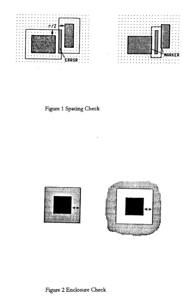
highlighted (see Figure1). Minimum feature sizes can bechecked on alayer
by
shrinking
by
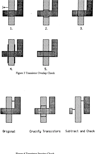
halftheminimum sizeforthelayer. Enclosurechecks of onelayeraround another, such as contact cuts, canbe calculated as aminimum spacing betweentheinside layerandthecomplement oftheenclosing layer (see Figure
2). To check transistor gate overlap, another type ofexpansion is used. Each
polysilicon edge is expanded in a perpendicular
direction,
then the overlap ischecked (see Figure 3). To prevent erroneous minimum spacing violations
from
being
detected,
where the polysilicon and diffusion lines run intotransistors, the expandedpolysiliconarea (calculatedabove for overlap) canbe
subtracted from the polysiliconlines before performing the minimum spacing
MARKER
Figure 1
Spacing
Check1'U.liw^Ji.i '.i.Li..nuiit^
4.
5.
Figure 3 Transistor
Overlap
Checki
^
s
^
liljli
lIlN;
iillili
I
IB
Original
Crucify
Transistors
Subtract
andCheck
Rules that check contact overlap and transistor spacing require Boolean
operations to be performed on the input mask layers. It is simpler to first
perform the Boolean operations on the layers to derive the transistor,
transistor-overlap,
and contact area pseudo-layers. Then the minimum widthand spacingrules canbeperformed usingthesenew pseudo-layers. The design
rule checkis therefore a two step operation, one step to derive the
pseudo-layers,
andonestepto checkthewidth andspacings of allthelayers.A design rule language is used to describe the derived pseudo-layers and the
design rule specificationsfor the process. Three typesofdesign checks canbe
defined: widthchecks, spacingchecks,and enclosure checks. Width checksare
defined
by identifying
thelayer,
theminimumwidth andthe rulename; spacingchecks are defined
by
identifying
the twolayers,
the spacingdistance,
and therulename; enclosure checks aredefined
by
specifying theinternal and externallayers,
theoverlap,andtherulename.Whenthedesignrule checkerisinvoked,
the definition file for theprocessis read
in,
and the derived pseudo-layers arecreated. Onthesecondpassthedesignrulesare checked.
The output error edges can be reported as a new error layer that can be
overlaid on the original design layout. Ifa separate error cell is reported for
each type ofdesign rule error, then the user can view one type of error at a
time,
such asmetal-to-metalspacing.Circuit extraction consists of
finding
the transistors, the nets between thetransistors, and the transistor areas and perimeters to calculate capacitance
estimates and transistor size. The outputis a list oftransistors, their size and
types, a netlist with the connections between their gates, sources and
drains,
and alistofcapacitorsfromthenetstogroundorbetweennets.Theestimated
accurate circuit simulations. The netlist generated can be compared with the
circuit schematictoverify logic and schematicare equivalent.
In MOS circuits, transistors are created
by
crossing polysilicon and diffusionlayers. Different typesoftransistors aredetected
by
thepresence orabsence ofimplants and wells. The definitions of the pseudo-layers that comprise the
different transistor types for a fabrication process are added to a
technology
file,
similarto the design rule checkertechnology
file. Once each transistorisuniquely identifiedand thenodes are numbered, the connections between the
nodes are examined. Connections are preserved over continuous runs on a
layer and through contacts connecting two layers. Incorrect transistor ratios
and malformed transistors with
floating
nodes or shorts between power andground can be identified with a simple electrical rules check. Transistor drive
size is calculated
by determining
thewidth and length ofthe transistors. Forrectangular transistors, the width is the one half the perimeter with the
diffusion edge, and the length is one half the perimeter with the polysilicon
edge.
Parameter extraction determines the electrical parameters from the layout for
use in refiningthe circuit simulation timing. Thetwo categories ofcapacitance
that can be calculated
during
extraction are area and perimeter capacitance tosubstrate, and the capacitance between parallel wires or nodes. Each wiring
layer and transistor type has a differentcapacitance
factor,
whichis a functionofthe fabrication process. These factors are added to a
technology
definitionfile for the process, similar to the design rule checker
technology
file.During
extraction, theareas andperimeter foreachlayerare calculatedseparatelythen
multiplied
by
the appropriate scalefactor,
and the result is totaled to get aWiring
resistance canbe calculated forlong
parallel lines as the length oftheparallel
lines,
dividedby
the distance between them, times the resistance scale factor for the layer. Transistor resistance is proportional to the length overwidth ratio (the inverse ofthe
Z-ratio)
ofthetransistor, times the scale factor fortheprocess.Generally,
atthetimeofthisproject,mostcircuit extractorsdonot calculatewiringresistance for back annotating intothe circuitdesign dueto thelargenetworkofresistors thatwouldresult9.
IV.
Materials
andApparatusA, Mentorand
Cadence Tools
The additional standard cells for the RIT CMOS standard cell
library
and themorphological array controller chip set were designed on HP/Apollo
workstations running theAegis operating system.
The
RIT CMOS standardcell
library
has already been integratedwithversion 7.0oftheMentor Graphics toolsuite as apartofLarry
Rubin'sthesis1.The Mentor Graphics development tool suite consists of the Neted schematic capture tool, the Quicksim logicsimulator, the Accusim SPICE circuit simulator, the Cellgraph cell automatic place and route tool, and the Chipgraph hand layout editing tool. In addition the Cadence Dracula II design rule checker
(DRC),
electrical rule checker(ERC),
layoutversus schematic(LVS),
and layoutparameter extraction(LPE)
tool suite will be utilized. The Mentor Graphics tool suite is licensed and
available on all ofthe HP/Apollo workstations in the lab. The Cadence tool
suiteis only licensedtorun on twoworkstations withinthelab.
When a top-down design methodology is used, the design process is divided
circuit
design,
and physical design. These design representations are used todescribe different levels ofabstraction ofthe system. The design automation
process consists of a series of iterations of, and conversions
between,
thesedifferent representations of a system.
Mamtaining
equivalency across thedifferent design representations is an important issue for design automation
tools.
The design specification stage is the manual process ofspecifying the system
requirements. The behavior of the system, as a function of the inputs and
outputs,is described
during
functional design. Logicand circuit design describethelogicalor schematic structure ofthe systemtomatchthe functionaldesign.
Physical design involves converting the circuit structure into the format
requiredtomanufacturethephysicaldevice.
Each of the design phases may be composed of synthesis, analysis, and
verification steps and therefore the design automation tools utilized
during
these steps can be categorized as synthesis, analysis, or verification and
validation tools9. Synthesis tools generate a new representation of a
design,
such as the Mentor Graphics Cellgraph automatic place and route tool.
Analysis tools evaluate the consistency or correctness of a design
representation. The Cadence designrule checker
(DRC)
is an example of suchatool, it checks thephysicallayout for geometric ruleviolations. The Cadence
electrical rule checker
(ERC)
is another example, it checks that the circuitextractedfrom the layout does not have anyelectrical errors such as shorts or
floating
nodes. Verification tools provide a formal method fordemonstrating
the equivalence of two design representations. The Cadence layout versus
schematic
(LVS)
tool verifies that the circuit extracted from the layout isequivalent to the circuit design representation. Validation demonstrates the
equivalence oftwo designs usingalimitedsetoftest cases. Itis a less rigorous
In the functional design stage the functional behavior of the design is represented. This may consist of
timing
charts, blockdiagrams,
or behavioral models. Mentor GraphicssupportsmodelswritteninC,
Pascal,
FORTRAN,
orVHDL. Behavioralsimulation with a series oftest vectors is used for analysis.
Mentor Graphics Quicksim was used for behavioral simulation. Logic design
involves
implementing
the functional design at the gate logic level using aschematic diagram. The logic design is validated against the functional design
by
comparing
the results of the behavioral simulation with the logicalsimulation. Mentor Graphics Neted was used for schematic capture and
Quicksimwasonce again usedfor logic simulation,using aunitgate delay. The
circuitdesignphaseinvolves
implementing
thelogic design behaviorwithbasic circuit elements such as transistors and capacitors.During
the circuit designphase, transistors are sized to achieve drive and
timing
requirements andsubsequently the logic design may undergo some minor changes as the gates are sizedtomatchtheload. Netedwas usedtomake changesinthe schematic and the Mentor Graphics Accusim SPICE simulator was used for
timing
analysis.During
thephysicaldesignphase,thecircuitdesignwas convertedinto the geometric layout used in the fabrication process. The Mentor Graphics Cellgraph toolwas used for automatic synthesis (placement and routing). To hand layout the standard cells and correct unrouted and poorly routed lines resulting from a Cellgraph automatic place and route, the designer may useChipgraphto editthephysicallayout. Cadence
DRC, ERC,
andLVStoolswere used for analysis and verification. The layout is verified to conform to the designrulesby
the Cadence Dracula II designrule checker (DRC). The circuitextracted from the layout is checked for electrical errors such as shorts and
floating
nodesusing itselectricalrulechecker(ERC),
and verifiedtomapto thedesign,
and re-simulate the circuit for greater accuracy using Cadence DraculaIIlayoutparameter extraction (LPE).
Some of these design rule checking functions have recentiy been added
by
Mentor Graphics intheirREMEDI and Checkmateprograms. The Checkmate
tool has been installed and setup
by
ChuckCarline,
following
the completionofthelayout designwork on this thesis. Checkmate can perform
DRC,
ERC,
LVS,
and LPE functions similar to the Cadence toolsuite but it also has thesame limitation ofrequiring users to exit from Mentor Graphics Chipgraph
tool to run the checkers12. The advantage ofthe Checkmate installation over
the Cadence installation is that the software licenses are not node locked to
onlytwoworkstations,so
they
canrun on anyoftheHP/Apollo
workstationsin the lab. At this
time,
Checkmate LPE has not yetbeen configured for theMOSIS 2.0 pm N-well CMOS process. The REMEDI tool is a design rule
checker that Jeff Correll has integrated with the Chipgraph tools menus
through a set ofmacrosinvoked atChipgraph startup13. Because REMEDI is
invokedfromwithintheChipgraphtoolmenus, itprovidesamoreconvenient
firstpass designrule checkthan theCadence or Checkmate DRC tools,which
must be invoked after exiting out from Chipgraph. On the other
hand,
REMEDI should only be used as a first pass
DRC,
because it does not uselayoutnode data to skip same node checks or allow the definition of
pseudo-layers. Therefore Cadence DRC orCheckmate shouldstill be run on the final
layout. When used in conjunction with Cadence or Checkmate
DRC,
REMEDI can reduce the number ofinvocations of Cadence or Checkmate
DRC,
andtherefore the totallayout design time.A
series of scripts developedby
Shishir Ghate andLarry
Rubin,
designed towork in conjunction with the Mentor Graphics MCIF package, are used to
convert the final Chipgraph layout data into the Caltech Intermediate Form
B.
Tektronix
Logic Verifier
The
Tektronix
Logic Verifier 500(LV500)
can be used to efficiendy testcomplicated circuitdesigns. Thesystemthatis in currentoperation atRITcan
handle up to 64 different bi-directional signals. It can be driven
by
up to fourindependent
clocks (which can be distributed in anymanner). The LV500 isprimarily
used forthetesting
ofdigital circuits and has been enhanced at RITby
the addition ofa breadboard. With the breadboard an IC can bedirecdy
interfaced
to the LV500. Another useful feature of the LV500 is itscompatibility with the Mentor Graphics tools in RIT's VLSI Design
Laboratory.
Specifically
the application TekWAVES can be used to translateMentor Graphics test vector (event
driven)
format into the LV500's statedriven format.
Essentially
TekWAVES samples the event state changes fromthe HP/Apollo state file and creates an output file that matches the state
format and resolution ofthe LV500.
Thus,
one may design and test an ICusing Mentor Graphics tools, fabricate that IC with the aid of RIT's
Microelectronics facilities or
MOSIS,
and then test the circuit using the sametestvectorsthatwererunonthe HP/Apolloworkstations.
V. MethodofProcedure
The overall procedure ofthis thesisfollowedthese steps:
A. Write the Cadence Dracula II layoutverification systems
DRC, ERC, LVS,
andLPE
technology
(".com")
files fortheMOSIS SCN 2.0 pm N-wellCMOSB. Create additional
library
components and cells for the RIT CMOS standardcell
library,
as needed to complete the MorphologicalArray
ProcessorController
chip
set.C.
Layout
testchip 5 and6to test thefunctionality
ofthe RIT CMOS standardcell
library
MUXesandDflip-flop
cells.D. Design a Morphological
Array
Processor Controller chip setusingthe RITCMOS standard celllibrary.
1.The
functional
designarchitecture oftheMAP Controllerchip.2. Perform the
top
leveldesign
ofthe MAP Controller chip set architecture,andpartitionthechip set.
3. Performthelogic designoftheControllerand
Memory
Controller.4. Simulatethelogic designoftheControllerand
Memory
Controller.5. PerformthecircuitdesignoftheControllerand
Memory
Controller.6. SimulatethecircuitdesignoftheControllerand
Memory
Controller.7. LayouttheControllerand
Memory
Controller.8. Performthe designrulechecking
(DRC),
electricalrule checking(ERC),
andlayoutversus schematic
(LVS)
checkingonthelayouts.A.
Cadence
Dracula
IILayout
VerificationTools
Setup
Inthe designrule
theory
section,mentionwasmadeoftheneedfora separatetechnology
definition
file for each fabrication process anddesign rule checker;DRC, ERC, LVS,
and LPE. Also mentioned in thetheory
section, was theneed to define inthe
technology
files the input layers and pseudo layers usedby
therulescheckers, andthe specificdesignrules andparametervalues forthefabrication
process used. The MOSIS scaleable N-well CMOS(SCN)
processdenserules set revision6was chosentoallowformore compacteddesigns.
The first step involved with
defining
the DRCtechnology
file for the MOSISSCNprocess (see Appendix
A,
DRC.COMFile)
was todefinetheinputlayers,
the connection
layers,
and the connectivity relationship between the connectlayers utilized
by
the process. The connect layer definitions are utilized forsamenode checking. The *INPUT-LAYERto*ENDblockcontains theinput
and connectionlayer definitions. The CONNECT x y BYz statements define
the two layersto be connected,x andy, andthe connection
layer,
z. The nextstep involved
defining
a minimum set of pseudo layers to define n and ptransistorgates as wellasother
temporary
layersused to perform various ruleschecks suchas contactcut enclosure.Aminimum number oflayers is
desirable,
as each additional pseudo layer involves time and
memory
overhead. TheAND, OR, XOR,
and NOT statements are used to define the pseudo layers.The firsttwo layers specifytheinputlayers
(possibly
pseudo layersthemselves)
to perform the Boolean action upon, and the third layer the pseudo layer
created.Thefinal step involved
defining
a setofrules checksutilizingtheinputlayers and pseudo layers to check for each ofthe dense rule set violations. A
separate output error layer is specified to be created for each rule check
violation souserswillbeaware ofthedesignrule violated. WIDTH statements
define minimum width checks, EXT statements define minimum
checks, and ENC statements define enclosure checks. In the definitions the
OUTPUT
statement defines the output error cell layer. In most cases a singlecheck is sufficient, but for those rules with multiple possible error
combinations, such as rule 4.2 (pplus or nplus overlap of active), it was
necessary
to define an "a" and "b" set of rules checks to cover bothpossibilities. All of the rules checks were then verified using a test "chip"
consisting
of the specific examples from the MOSIS rev6 dense rule setdocumentation.
In some cases additional pseudo layers were defined tominimize false errors and improve error
detection,
particularly the SELECTtests. In specifying the error checks, it is preferable to err on the side of
generatingsomefalseerrors ratherthanmissinganactualerror.Users canthen
usetheirbest judgmenttoevaluatethose errors flaggedto determine ifan error
isa falseone.
The ERC and LVS
technology
file definitions (see AppendixB,
LVS.COMFile)
were ableto borrowtheinput layer andpseudo layer definitions fromtheDRC definition
file,
after removal ofthose pseudolayers created specificallytocheck for DRC rule violations that are unnecessary for definition of the
transistorswithin thelayout. Thenextstep for bothrule checkers wasto define
the transistor nodes using the ELEMENT statement. For ERC it was also
desirable to define the standard composite gate types, such as NAND and
NOR gates, so output errorreports would utilize thatinformationto simplify
and clarify output error reports, rather than reporting all output in terms of
individualtransistorsalone.
The LPE
technology
file definition (see AppendixC,
LPE.COMFile)
wassimilarto thatfor
LVS,
butalsoinvolveda steptodefinethepseudolayersthatwould be utilized for calculating parasitic capacitances and
diodes,
such asp
diffusion to
p
substrate capacitance. The PARASITIC CAP statementdefined
these capacitancetypes usingtheATTRIBUTE CAP statement,basedon data
supplied
by
MOSIS. It was also specified that the capacitances should be"smashed"
togetherintoa single valueforeach node. As the tooldidthisafter
calculating
eachcapacitance value separately,this turnedout to be a significantlimitation
of the tool, as only 500,000 capacitance values could be evaluatedpriorto"smashing". This limitedtheusefulnessofLPEtosmallerlayoutsonly.
B.
Additional Standard Cells
In the course of completing the design for the MAP controller chip set it
became necessary to design and layout additional RIT CMOS standard cell
library
components and cells. InparticularadditionalD flip-flops withbothQ
and
Q
bar outputs, and-or-inverts, or-and-inverts,CMUXes,
and MOSIS 64and 84pin pad rings were created (see Figure 5 through Figure 9). Each cell
design was
DRC, ERC,
and LVS tested before addition to the RIT CMOSA
IHhIM
^LfhHBhHSh-HM
^SHHS^
o d inHBhHHhHBhHSf
u z an-i itin:|D|
JJ-UJcu CJZ IU
.0
a-v. cn c CO >*
* in a CO V. ~* 0 CD 00 0 X C9 a *~> j:
3 L
C cn
0 H-l
. 1 oc
a* \ 3C
X c CJ
3 0 a
2: CO
a u 3 CM *
V
0 ** c 1 .c 2 ** **
3 s a I a a
.c c ""' a C TJ ip
5-^ShHl^
CX cnH8^BhH0hHSf
cn^ShHSP
CT cnHSr-H@hHShH0[
co cn cn cn
<J (Q)S <3 (DS
A
A
A
A
[image:45.549.43.513.45.644.2]c\j cn
B
LT
ilt
8
u
LT
A
cc X
J) c 3
fi
Cf
LT
a
o a
SVlCD
to
LI
cn
in
a a
cc ex
cc _1 a
cc
X
u
o a
ii
6
6)
0Q00
c\j cn =>
>(X)
[X) =>tX).. 4X) 5 i~Zi * t_r
sl =1 si
ST
=T
iocm coru
aTS=T =T sT =T
o
h
CD -.CM
> ,
2T
h
topj CVCM .
ru tow
CM
>z3 i
=T
T
IT CUM .
1
5
l<=T
ex
II
X li en
Li-CO
a CO X 2.
CT)
6A
ffl
17
7
TT
j
j
j
j
j
j
j
j
j
j
c3-H-t5|i>
J
I
C. Test Chips
5and6As a part of his thesis, Shishir Ghate was asked to verify the RIT CMOS
standard cell
library
designs and to calculate the internalnode capacitances ofthe designs for use in back annotating the standard cell circuit schematics.
Shishir performed the schematic design in Neted for the six test chips, along
with the layout and verification of four of the test chips2. The layout and
verification ofthe finaltwo test chipswas performed
by
the author. Test chipfive contains size A through C two-input
MUXes,
size A and B three-inputMUXes,
sizeA four-inputMUX,
size AandB five-inputMUXes,
andavarietyof D flip-flops (see Figure 10). Test chip six contains a variety of nMOS,
pMOS,andCMOStransfergates,individual
p
gate andn gate transistors,and avariety ofinverters (see Figure 11). Each chip was layed out and verified using
DRC,
ERC,
and LVS. Test chip four had an LVS error that the author wasunable to locate prior to shipment of the test chip layouts to MOSIS for
fabrication. This test chip contained some MUXes and D flip-flops whose
design was later changed for other reasons, so the loss was not appreciable.
Thereason forthe LVSerrors turned outto bea resultofthe automaticplace
and route tool. Cellstation did not always complete the placement of every
interconnectionline
during
cell routing. The author only became aware ofthisproblemlater
during
cellplaceandrouteforthecontrollerchip set,asthe toolserror message to this effect is difficult to find in the cell place and route
transcript.
Luckily
the author was then aware of this issue and was able toverifythecorrect automaticplace and routefor bothcontroller chips.
luS
Tm
ESS
; t s:
u
Tm
1 1in LU
CIS
I
X
JL
X J
i ' J3 TTT
"
3
i-LL JJ.
Isigi^
TTT!?-TTT
rN
h:!!1
^
!L
A
Ultf
J.S.I3
TTT
TTT TTT
S 33 ! ?
"sis' h:ir
TTT TTT
TSK t ! E
TTT TTT
5S!| :SiM| qV-l\ H!S=!| j|E;!|
fejis
fejiii
inj
iLij kLsj
iT iJT o
6
6
:! >
113
;Si=! :2PSj
O O O O D CD O
i-
J- J_ X ^
^oo
Hi
ITU
Oil
Oil ol rra \ttft
ft
ft
^a-c
,:,.^
a
I t * i.- t i. i- 1
5- S !
TTTTT iUiV
ids
TTTTT0
fin TTTTT ''"is1 ntrr TTTTT__ U_ tL_ Li- - U. LL.
ftk
rrp
ti? ?:.|!i 3e.g|' ?l-g!! TTT TTT TTThsir
HIT
Hit
HitHtf
HLtHfr
4LThg||? hsi?' hsls' Hsil1 hg.l1 hiSl' JlaSF
I I I|l 'liI ll 'liI|"| Mil I I III I ll I|| I I I
| |
____J_______ _. mdi .I -II .
ilt ilt
-117
ny
'iLj
-117117l_l w W
fTliTiii
ITT-Hi
l.iil
hH#]
FtliffflirtiT 5'elE' 2!:Ii' SisiS'
i#i
HP
1
TTT h|_|
|_plL.
*i ! * ? TTTTT|i=55, |5=I57
2,V .0
TT
TTT
*i I S3
ts
IJOai
_ec -tu 3U LEE UJ a X3
0 _: a i 31
.! L > r _.0 3 IO j - C 3 S OD. Morphological
Array
ProcessorController Design/.
The Functional
Design Architecture oftheMAP ControllerChip
The implementation ofamorphological operation is accomplished
by
movingawindow composed ofpatterning elements over an image. The target image
pixelis the pixel underthe center window element. Operations are performed
onallpixelswith awindowvalue abovethem,withtheresultingvaluereplacing
the originaltargetpixelvalue.
When the construction of a Morphological Image Processor prototype was
proposed,itwasdecidedthat theimagewouldbe 512x512pixels usingan 8-bit
gray scale pixelrepresentation, with an extra bit used to represent undefined
pixels (shown as * in the Morphological
Theory
section). These undefinedpixelscanbe implementedandtreatedasif
they
were negativeinfinity (-00)
andwill be represented as such in future references. The
meaning
of negativeinfinity
was discussed in the MorphologicalTheory
section and since it waspossible to use the extrabit to also represent negative pixel values,
they
wereincluded incase a use is ever found forthem. Table 1 shows the
binary
pixelvalues and their corresponding decimal values. Negative values use the two's
complement representation, with negative
infinity
using the value that wouldnormallyrepresent-512. Sincemostimage capture and
processing
systemscanonly dealwith 8-bit grayscale images andhaveno concept of negative
infinity
and negative pixelvalues, the 9-bit gray scale system will be referred to as an
patterning
elements, also using the extended 8-bit gray scale pixelrepresentation.
Binary
Decimal 0 0000 0000 00 0000 0001 1
0 0000 0010 2
; I
01111 1101 509
01111 1110 510
01111 1111 511
1 0000 0000 -00
1 0000 0001 -511
1 0000 0010 -510
:
i mi noi -3
i mi mo -2
i mi mi -1
Table 1
Binary
PixelValues andTheir Decimal EquivalentsWhile choosing an architecture for the Morphological Image Processor
prototype, therewere a fewgoals thatweredesirable to achieve. One ofthese
goals was to allow the processor to operate at areal-time rate (60 images per
second) using the same 512x512 pixel extended 8-bit gray scale images and a
7x7window.
Implementing
thedesign usingaVLSI circuitis currentlythebestway to achieve the real-time rate, so a regular structure was desirable to
facilitate aVLSI layout. Another goalwas a simple controlsection to facilitate
expansiontolargerwindow sizes andlarger images.
Also,
the processor shouldbe designed such thatit is easy to pipeline withidenticalprocessors and allow
theinputs and outputs to be connected to real-time sources and
destinations,
possiblywith some
buffering
to make the system compatible with interleavedForthe Morphological Image Processorprototype,a 512x512 imageand a 7x7
windowwere used,so all examples and explanations will use these sizes,unless
otherwise noted. All ofthe concepts discussed in this section will work with
any size image and window as
long
as appropriate adjustments are made. Allindexvalueswillstartat0 and end atthe oneless than themaximumvalue, for
example, the
top
left ofa 512x512 image will be referred to asX00
and thebottom right ofthat image will be referred to as
X511>511,
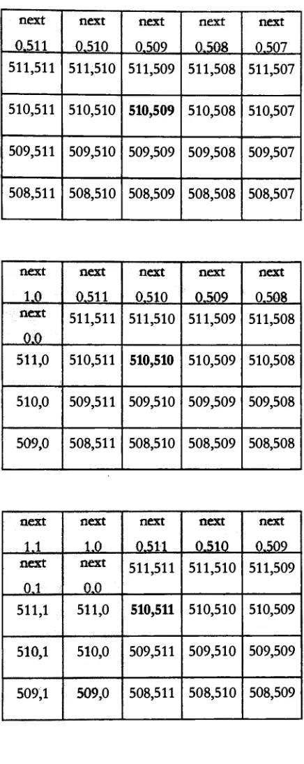
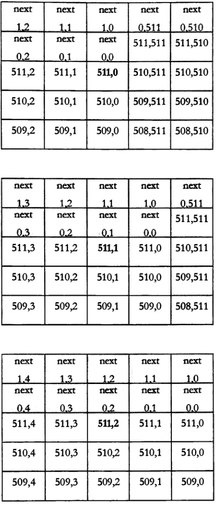
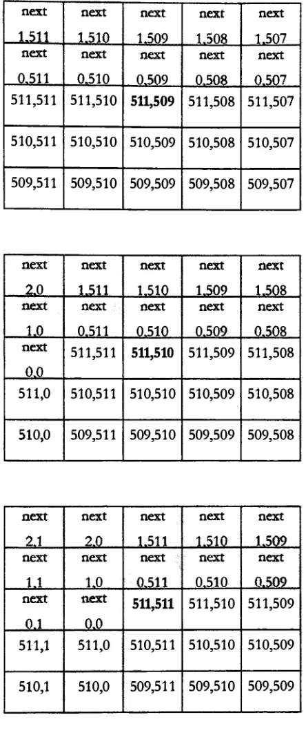
with the first indexvalue
referring
tothe rowandthesecond oneto thecolumn.As
previously
discussed intheMorphologicalTheory
section forequations(39)