Theses Thesis/Dissertation Collections
5-13-2010
Design, development and simulation of
sub-lithographic process for patterning nm scale
features
Guriqbal Singh Josan
Follow this and additional works at:http://scholarworks.rit.edu/theses
This Thesis is brought to you for free and open access by the Thesis/Dissertation Collections at RIT Scholar Works. It has been accepted for inclusion in Theses by an authorized administrator of RIT Scholar Works. For more information, please [email protected].
Recommended Citation
A thesis submitted in
partial fulfillment of the requirements for the degree of Masters of Science in
Microelectronic Engineering
By
Guriqbal Singh Josan
Electrical & Microelectronic Engineering Department Kate Gleason College of Engineering
Supervised by:
Professor Santosh K. Kurinec, PhD
Electrical & Microelectronic Engineering Department Kate Gleason College of Engineering
Rochester Institute of Technology Rochester, New York
KATE GLEASON COLLEGE OF ENGINEERING
ROCHESTER INSTITUTE OF TECHNOLOGY
ROCHESTER, NEW YORK
________________________________________________________________________
CERTIFICATE OF APPROVAL
MASTER OF SCIENCE DEGREE THESIS
________________________________________________________________________ A thesis entitled
Design, D
evelopment and Simulation of Sub-Lithographi
c
Process for Patte
rning nm Scal
e F
eatur
es
by
Guriqbal Singh Josan
The Masters of Science Degree Thesis of Guriqbal Singh Josan has been examined and approved by the thesis committee
as satisfactory for the thesis requirement of a Master of Science degree
We the undersigned have had the opportunity to attend, question, and discuss the FDQGLGDWH¶VSUHVHQWDWLRQRIUHVHDUFKUHVXOWVXSRQZKLFKWKLVWKHVLVLVEDVHG:HEHOLHYH this work constitutes satisfactory completion of the requirements for a Master of Science degree.
Dr. Santosh K. Kurinec _________________________ Date: ________________ (Thesis Advisor- Professor Microelectronic Engineering)
Dr. Sean L. Rommel __________________________ Date: ________________ (Committee Member- Professor Microelectronic Engineering)
Dr. Robert E. Pearson __________________________ Date: ________________ (Committee Member- Program Director, Microelectronic Engineering)
by
Guriqbal Singh Josan
I, Guriqbal Singh Josan, hereby grant permission to the Wallace Memorial Library of the Rochester Institute of Technology to reproduce this document in whole or in part such that reproduction will not be for commercial use or profit.
The author would like to acknowledge the faculty of the Department of Microelectronic Engineering at the Rochester institute of Technology for providing an invaluable education and hands-on experience in semiconductor manufacturing. The success of this thesis is attributable to the support and guidance of following persons:
Professor Santosh K. Kurinec, a great professor and a human being who always provided me with an endless inspirational support, knowledge and guidance throughout my graduate career. I am thankful to her for the continuous encouragement in every facet for the completion of this thesis.
Professor Sean L. Rommel, who gave me key suggestions and advised me on how to proceed with the challenges met during this work as my committee member. His contributions in guiding me on the use of scanning electron microscope are unforgettable. Professor Robert E. Pearson, for serving on my thesis committee and bringing a different viewpoint that helped in a deeper understanding of the pursued research work
In addition, special gratitude is due to Professor Karl D. Hirschman, for providing the knowledge in semiconductor process & device modeling and Professor Lynn F. Fuller, for helping me appreciate and understand semiconductor manufacturing.
The author appreciates the interest and help of a PhD graduate student Archana Devasia in this project.
The author further acknowledges the valuable technical support provided by Bruce Tolleson, Scott Blondell, Tom Grimsley John Nash and Dave Yackoff during the use of facilities in the RIT Semiconductor & Microsystems Fabrication Laboratory (SMFL). Special appreciation LVGXHWR6HDQ2¶%ULHQIRUKLVLPPHQVHKHOSLQDQVZHULQJ process related questions.
The author is extremely thankful to Keith Fogel of IBM Watson Research Center and Brian McIntyre of University of Rochester for their help in cross sectional scanning electron microscopy extensively employed in this study.
The process simulation work carried out in this study has been made possible by the generous donation of TCAD tools by Silvaco to the Microelectronic Engineering program at RIT.
The ability to create sub-lithographic nm-scale features without the need of high-end lithography tools will create new opportunities for the electronics industry. Most current technologies are lithography dependent and inherit associated CD variations.
Dedicated to my parents,
Title Page «««««««««««««««««««««««««««««««i
Certificate of Approval «««««««««««««««««««««««««ii
Library Release Declaration ««««««««««««««««««««««iii
Acknowledgements ««««««««««««««««««««««««««Lv
Abstract ««««««««««««««««««««««««««««...v
Table of Contents«««««««««««««««««««««««««.vii List of Tables ««««««««««««««««««««««««« ...««ix
List of Figures«««««««««««««««««««««««««««««x 1. Introduction and Motivation...1
1.1. Motivation...3
1.2. Summary and Organization of Thesis...5
Chapter 1: RHIHUHQFHV«...6
2. Theory««««««««««««««««...8
2.1. Non-Conventional Patterning Techniques: A literature Review...9
2.1.1. Spacer Patterning Technique (SPT)...9
2.1.2. Lift-off Process ...10
2.1.3. Electroplating««««««««««««««««««««.12 2.1.4. Ashing & Trimming ««««««««««««««««««13 2.2. Disadvantages of Existing Non-conventional Patterning Techniques...14
2.3. Keyhole Patterning Technique««««««...15
2.4. Thin-Film Deposition«...17
2.4.1. CVD Thin Film Growth Mechanism««...«« 2.4.2. Structure and Properties of CVD Thin films«...21
2.4.3. Basic Characteristics of CVD and Deposition Conditions««« 2.4.4. Different types of CVD reactions...35
2.4.5. Low-Pressure Chemical 9DSRU'HSRVLWLRQ/3&9'««« 2.4.6. Plasma Enhanced Chemical Vapor Deposition (PECVD)««« 2.5. Comparison between Wet and Dry Etching««««««««««« 2.5.1. Important Etch Terminology«««««««««««««« 2.5.2. Dry Etching««««««««««««««««««««« 2.5.3. Reactive Ion Etching (RIE)««««««««««««««« 2.5.4. Dry Etch Gas Selection«««««««««««««««« 2.5.5. Dry Etching Si/ SiO2 in Fluorine Based Gases and Plasmas«« 2.5.5. Etching Trend Chart for different materials««««««««« Chapter 2: RHIHUHQFHV«...54
3.3.1. Process Development««««««««««««««««« 3.3.2. Stack Formation (Thin Film Deposition) «««««««««« 3.3.3. Photolithography Optimization««««««««««««« 3.3.4. Dry Etch Process Development: Process Flow Step 2««««« 3.3.5. Overhang Formation: Process Step 3««««««««««« 3.3.6. Polysilicon Deposition: Process Step 4«««««««««« 3.3.7. Void etch-back for Pore Definition: Process Step 5«««««« 3.3.8. Left-over Polysilicon and SiO2 Wet Etch: Process Step 6«««
3.4. Process Flow«««««««««««««««««««««««
3.5. &KDSWHU5HIHUHQFHV«...84 4. 3URFHVV6LPXODWLRQVDQG([SHULPHQWDO9HULILFDWLRQ«««««««««
4.1. Elite Topography Simulator ««««« «««...86 4.1.1. Process Simulation MethodRORJ\««««««««...88 4.1.2. Deposition Models in Elite«««««««««««««««..88 4.1.3. Etch models in Elite««««««««««««««««««90 4.1.4. Simulation Physics«««««««««««««««««« 4.1.5. Etch Rate Calculations«««««««««««««««« 4.2. Simulation Results««««.««««««««««««««««.93 4.3. Experimental ProceGXUH«««««««««««««««««« 4.4. Experimental Verification «««««««««««« 4.5. Simulation Model Calibration««««««««««« 4.5.1. Stack Trench Etch and CVD model calibration«««««« 4.5.2. Void Etch-back Calibration««««««««« 4.5. Proposed Unified Simulation Model««««««« 4.6. Chapter 4: References«««««« 5. Conclusions and Future Work ««...107
5.1. Potential Applications for Void-assisted Pattern Transfer Process...108 5.2. Future Work«... «««««««
5.3. Chapter 5: References «««««... «
$SSHQGLFHV«« «113
Appendix III. Process Details/ Recipes««««««113
Table Description Page
2.1 Comparison between wet and dry etch 38
2.2 Dry etching spectrum with typical etching characteristics 48 2.3 Typical etch chemistries and the byproduct of dry etching reactions 48 3.1 Final pore diameter for different values of overhang and sidewall
angle (Fixed R=500 nm)
61
3.2 Details of parameter employed in approach I for dry etch process
development 69
3.3 Different etch parameters used in approach I. Best LPCVD Si3N4/ annealed PECVD SiO2 etch selectivity ever reported at RIT using flouring based chemistry with high degree of anisotropy in this work
71
3.4 Details of parameters employed in approach II for dry etch process development
72
3.5 Different etch parameters used for anisotropic PECVD SiO2 etch in P5000 MERIE Chamber C
73
3.6 Details of various parameters used in Aluminum etch recipe 76 3.7 Details of various parameters used in Polysilicon etch recipe 80 3.8 Complete process flow for void transfer patterning process 83 4.1 Model parameters used for simulation model calibration 102 5.1 Summary of design and process integration related issues and
proposed solutions
Fig. Description Page 1.1. Comparison of trends in the wavelength of exposure light and the
minimum feature size 2
2.1 Nanotechnology roadmap from 1940-present. The figure illustrates the
possible regime for non- conventional patterning and this work 8 2.2 Schematic diagram of the process flow for; a) single spacer; b) multiple
spacers for nanowires
9 2.3 Process flow for producing polysilicon nanogaps using spacer
lithography 10
2.4 Process flow schematic: Liftoff process 11
2.5 SEM micrographs showing (left) PMER line after ashing, (right) smallest 20 nm gap formed after lift-off process
12 2.6 CD variations as function of electron dose for gold structures plated in
400 nm and 150 nm resist 13
2.7 Process flow schematic for Ashing and Trimming process 14 2.8 CD variations for three different nano-length scale (NLS) patterning
techniques 15
2.9 6FKHPDWLFRIDSURFHVVIORZIRUDµSRUH¶3&0FHOO)LJXUHRQULJKWshows keyhole parameter calculations
15 2.10 (left) SEM cross-sectional image after step 3 in process sequence
showing similar sized keyholes voids in 250 nm and 315 nm initial holes, (right) STEM image of the final pore after step 5
16
2.10(c) Sequence of SEM micrographs showing successful transfer of keyhole
into SiN 17
2.11 Different thin-film deposition techniques 18
2.12 Generalized sequence for thin film growth mechanism for CVD deposited films
20 2.13 Quantitative representation of the influence of various deposition
parameters on grain size of thin films
22 2.14 Qualitative variation of roughness factor with film thickness for lower
and higher temperatures 23
2.15 Scanning electron micrographs showing surface of rough and smooth films; a) obliquely deposited GeSe film; b) rough CdS film; and c) smooth CdS film with conditions optimized to deliver lower surface roughness
24
2.16 Thin film density as a function of film thickness for low and high
substrate temperature (TS) 24
2.17 Tape test performed to check adhesion; proper adhesion (left) and poor adhesion (right). The film on the right was deposited by evaporation, which is frequently linked with film de-lamination problems.
stress
2.19 Effect of temperature on type of film stress. Thermal annealing alleviates both tensile and compressive stress
29 2.20 Tensile stress producing concave curvature of the substrate (left),
compressive stress resulting in convex curvature (right) 29 2.21 Low pressure and longer mean free path results in fewer collisions
delivering high-energy particles. Whereas, at higher pressures, more particles are present, mean free path and ion energy are lower
30
2.22 Typical film stress variation as a function of pressure 31 2.23 SEM image for quality of film using straight-DC power supply (left)
And using pulsed-DC power supply (right) ²Higher ion energy produces better film uniformity, smoother film and greater packing density
32
2.24 Stress in CVD deposited film as a function of power 32 2.25 Growth rate of CVD films as a function of temperature 34
2.26 Schematic of a typical LPCVD system at RIT 35
2.27 A typical PECVD system schematic 36
2.28 Etch profiles corresponding to different lateral etch ratios (RL) 38 2.29 Pattern transfer for different lateral etch ratios (RL) during wet etch 39 2.30 The progression of the etched feature with finite mask etch rate (mask
erosion). The CD loss is twice the bias width and is given by µ:¶ 40 2.31 Corner faceting. The sputter action creates angled facets that propagates
down with the eroding mask causing sloped etch profiles
41 2.32 Plasma etching mechanism with the sequence of processes 43
2.33 Schematic of a typical parallel plate RIE system 45
2.34 Various Plasma parameters affecting the reactive-ion etching process. 46 2.35 Normalized etch rate of Si and SiO2 versus the O2 concentration in CF4 ±
O2 gas
49 2.36 The etch rate of resist, SiO2 and poly-Si in a RIE configuration versus H2
concentrations in CF4 - H2 feed gas system
50 2.37 The boundary between etching and polymerization conditions influenced
by F/ C ratio of reactive species and the applied bias 51 2.38 Surface inhibitor mechanism for ion assisted anisotropic etching 52
2.39 Etching trend chart for different materials 53
3.1 Void patterning process flow schematic 57
3.2 9RLGSDUDPHWHUVDQGGLDPHWHUFDOFXODWLRQVµǻ¶UHSUHVHQWVWKHRYHUKDQJ µș¶UHSUHVHQWVWKHVLGHZDOODQJOHµD¶ is the final void diameter, µr¶LVKDOI the lithographic defined hole (i.e. U 5DQGµL¶LVthe void length
58
3.3 Test mask designed using Mentor Graphics mask layout editor and MEBES III electron beam mask writer
62 3.4 Fig. 3.4. SEM image for the low stress PECVD stack (SiN-SiO2-SiN)
deposited using Applied materials P-5000 (Chamber A and B), and corresponding process flow schematic step 1.
widely spaced features. The pitch varies from a) 1, b) 1.5, c) 2.5, d) 5.5 and e) 10.5 µm as seen in the figure
3.6 Aluminum etching results using initial resist profiles resembling 66 3.7 Reflected component from different interfaces in SiN-SiO2-SiN stack: a)
reflection from top SiN-SiO2 interface, b) reflection from SiO2- bottom SiN LQWHUIDFH/LWKRJUDSK\VLPXODWLRQGRQHXVLQJµ3UROLWK
68
3.8 Optimized resist profiles for varying density. The pitch varies from 1 µm, 1.5 µm, 2.5 µm and 5.5 µm. Figure (d) still shows the rounding of resist tops associated with reflow during post development bake (hard bake)
70
3.9 (a-c) SEM images showing etch results for approach I, (d) process flow
step 2 70
3.10 SEM images showing highly anisotropic stack etching for a pitch of a) 1 m, b) 2.5 m, c) 1.5 m, and d) 5.5 m
73 3.11 Micro-loading effects affecting the MERIE etch rates for unannealed
PECVD oxide. Density varies as 0.5, 2, 5 and 10 m and feature size varies from 0.5, 0.75, 1 and 10 m. All measurements are approximate and derived from SEM images
74
3.12 SEM image showing that the Aluminum etched anisotropically using the recipe developed in this work
75 3.13 Process flow schematic step 3 (left), SEM image showing the overhang
formed in oxide layer (right). 77
3.14 Process flow schematic step 4 (left), SEM image showing the void formed in polysilicon (right). The combined effect of overhang and the conformal polysilicon deposition pinches off at top to intentionally form bottle shaped voids
73
3.15 SEM micrograph showing conformal nature of 610 poly recipe 79 3.16 Process flow schematic step 6 (left), SEM micrograph showing the void
etch-back in progress (right, bottom) 79
3.17 Process flow schematic step 6 (left) and the actual SEM micrograph displaying the small pore defined in SiN layer after the polysilicon and SiO2 etch (right).
81
4.1 ATHENA Architectural Framework with different interfaced modules 86
4.2 String Model approximation to the Etch Front 87
4.3 (left) Etch-front motion due to directional influence, (right) areas of significance of rIso and rDir where shadowing effect is accounted for by the rIso component in the shadowed area.
90
4.4 Comprison of etch profiles for Monte Carlo and plasma etching models
using oxide as etch hard mask 91
4.5 Compiled simulation results for the void patterning technique. Overhang ǻaQPWKHYRLGVL]HµD¶aQPDQGsub-lithographic pore has diameter of 200 nm
94
4.7 (IIHFWRIVLGHZDOODQJOHµ ¶ RQNH\KROHGLDPHWHUµ'¶'HFUHDVHLQµ ¶ PDQLIHVWVGHFUHDVHLQµ'
96 4.8 SEM micrograph showing a contaminant particle masking a portion of a
die during void transfer etching
98 4.9 Fig. 4.9. X-SEM image of (a) void formed, (b-f) polysilicon etch-back
and (g) final Sub-lithographic aperture 99
4.10 Simulation model calibration showing effects of variation in parameters on trench profile and void formation. Row (1) shows the effect of Ki and Kf, row (2) shows the effect of pressure, row (3) shows the effect of Vpdc and row (4) shows the profile obtained using experimental values and the experimental X-SEM image
101
4.11 Simulation model applied to reproduce the work done in [7]. SEM picture (a) adapted from reference
102 4.12 Model calibration results and the illustration of moving etch interface in
comparison with experimental X-SEM images of the void transfer in progress
103
4.13 The proposed unified simulation model flowchart for void transfer
patterning technique 105
5.1 Schematic of two neighboring unit cells and TEM image of pore
memory cells above FET access transistors (left) and 256kbit functional test array (right)
109
5.2 The keyhole process greatly reduces the spread expected from a conventional spacer process under the same CD variations
109 5.3 Fig. 5.3. Various applications of nanogaps formed using spacer process 110 5.4 Voids formed in polysilicon can serve as fluidic channels for MEMS or
NEMS based application
111 5.5 Cross-sectional schematic of a proposed single celled PCM device (left)
and top view (right). 112
C H APT E R 1
Introduction and Motivation
The relentless drive for smaller, faster and cheaper devices has pushed the
existing semiconductor technology to their limits. In the past decade lithography
technology has been the key driving force for the phenomenal rate of increase in the
integration density of silicon-EDVHG PLFURHOHFWURQLFV FLUFXLWV IROORZLQJ 0RRUH¶V ODZ.
However, miniaturization based on optical lithography wavelength reduction has already
hit a roadblock. There are many post-optical era lithography contenders capable of
patterning down to nano-scale - such as Extreme ultraviolet lithography (EUV), Electron
projection lithography (EPL), Multicolumn direct-write E-beam, Scanning probe arrays,
Nanoprinting, Scattering with angular limitation projection electron-beam lithography
(SCALPEL), X-ray lithography and Immersion Lithography [1-3]. The applications of
these technologies may not be financially viable for small manufacturers and researchers
and for products to compete in the market.
Nonetheless, the incessant appetite for the evolution of semiconductor devices has
pushed researchers to look into other non-conventional nano-patterning techniques in
order to understand the effects and properties at nanometer scales. Figure 1.1 shows the
evolutionary trends comparing the minimum critical dimensions (CD) and wavelength of
the exposure source. The slope of miniaturization trend is steeper than the rate at which
exposure wavelengths have been reduced, illustrating the increasing practical importance
1.1. Motivation
The ability to create sub-lithographic nm-scale features without the need of high-end lithography tools will create new opportunities for the electronics industry and an immense resource for future projects at RIT that require nano-features.
As the flash memory scalability is nearing its limits, the phase change memory (PCM) based on variable resistance contrast is at the forefront of research. Better performance, scalability [4], larger cycling endurance [5] and faster read/write time have been reported. However, with the projection of increasingly smaller cells for future technology, PCM technology can succeed only if it continues to promise the scaling trends for many future generations. The greatest challenge in designing large-scale PCM arrays for commercial use is the requirement of high programming current densities (>107 A/cm2 as compared to 105-106 A/cm2 for transistors). This means that an active area needs to be scaled much smaller than the transistor area in the driving circuit. Many recent attempts detailing feasible scaling technologies involved in realizing the prototype to large scale production of these chalcogenide based PC-RAMs have been already reported in literature [6-10]. Nonetheless, a more reliable technique to form nanometer-sized structures with the extreme scaling potential is required for the realization of such next generation nano-electronic devices.
[14], resist ashing and trimming [15], electroplating [16] and lift-off process [17]. But, all these technologies are lithography dependent and inherit associated CD variations. This is extremely crucial for memory applications where even subtle CD variations affect vital device characteristics such as retention time and endurance.
The mainstay of this work is mathematical modeling, simulation and verification of a revolutionary µVoid Transfer Patterning Process¶ for nm scale features. This process was originally introduced by Breitwisch et al. [18] to demonstrate a fully integrated 256
1.2. Summary and O rganization of Thesis
C H APT E R 1: Re
fe
r
ences
1. T. Ito, 6 2ND]DNL ³3XVKLQJ WKH OLPLWV RI OLWKRJUDSK\´Nature, Vol. 406, 31 Aug 2000.
2. L.R. Harriott, "Limits of lithography," Proceedings of the IEEE, vol.89, no.3, pp.366-374, Mar 2001
3. G.F. Cerofolini, G. Arena, M. Camalleri, C Galati, S. Reina, L. Renna L, D.
0DVFRORDQG1RVLN³6WUDWHJLHVIRUQDQRHOHFWURQLFV´Microelectron. Eng. Vol 81, Issues 2-4, August 2005, P 405-419
4. Pirovano A, Lacaita A.L³6FDOLQJDQDO\VLVRISKDVH-FKDQJHPHPRU\WHFKQRORJ\´ IEDM Tech Dig, 2003. p.699±702
5. Pirovano A, et al. ³5HOLDELOLW\ VWXG\ RI SKDVH-change non-YRODWLOH PHPRULHV´ IEEE Trans. Dev. Mater Reliab 2004; 4:422±7.
6. Lacaita A.L, HW DO ³Phase change memories: State-of-art, challenges and
SHUVSHFWLYHV´Solid-State Electron. Volume 50, Issue 1, January 2006, Pages 24-31
7. K.A. Campbell, Microelectronics Journ. 38, pp. 52-59, 2007. 8. A. Redaelli et al,IEEE Elec. Dev. Lett., vol. 25, pp. 684-686, 2004 9. S. Raoux et al, MRS Bulletin, vol. 33, pp. 847-853, Sept. 2008.
10. 65DRX[³Phase-FKDQJHUDQGRPDFFHVVPHPRU\$VFDODEOHWHFKQRORJ\´IBM J. Res. & Dev. Vol. 52 NO. 4/5July/Sep. 2008
11. H.I. Smith, D.C. Flanders, J. Vac. Sci. Tech. 17 (1980) 533.
12. J. Kedzierski, P. Xuan, E.H. Anderson, J. Bokor, T.J. King, IEDM Tech. Dig. (2000) 57.
13. L.E. Erickson, P. Schmuki, G. Champion, J. Vac. Sci. Technol. B. 18 (2000) 3198.
14. Y.K. Choi, T.J. King, C. Hu, IEEE Trans. Elec. Dev. 49 (2002) 436.
15. K. Asano K, Y.K. Choi, T.J. King, C. Hu, IEEE Trans. Elec. Dev. 48 (2001) 1004.
16. G. Simon G, A.M. Haghiri-Gosnet, F. Carcenac, Microelec. Engg. 35 (1997) 51.
18. M. Breitwisch et al, ³ 1RYHO /LWKRJUDSK\-Independent Pore Phase Change 0HPRU\´Symp. VLSI Tech., 2007.
19. S. Takagi, K. Iyanagi, S. Onoue, T. Shinmura, M. Fujino, Jpn. J. Appl. Phys. 41 (2002) 3947.
20. $WKHQD8VHU¶V0DQXDO9
C H APT E R 2
Theory
Miniaturization based on optical lithography wavelength reduction has already hit a roadblock and the changeover to newer technology is financially constrained. Figure 2.1 shows the nanoWHFKQRORJ\ URDGPDS VLQFH ¶V LOOXVWUDWLQJ GLIIHUHQt approaches incorporated for crossover to nanotechnology. Solutions for features below 180 nm are Electron-beam (e-beam) lithography [1, 2], X-ray lithography [3], Focused ion beam lithography [4, 5] etc. But, these techniques lack in line-width homogeneity over the whole wafer, offer lower throughput, and are time consuming, complicated and expensive. Thus, their exploitation in integrated circuit processing is still putative. However, with the invention of some revolutionary techniques, patterning of sub-lithographic features is still feasible and in-fact very widely used in industry.
2.1. Non-Conventional Patterning Techniques: A Literature Review
Some of the non-conventional patterning techniques include Spacer patterning
technique (SPT) [7-9], lift off process [10], Electroplating [11] and Ashing and trimming
[12]. These techniques are briefly discussed as follows.
2.1.1. Spacer Patterning Technique (SPT)
The SPT [7-9], [13] incorporating the use of conventional optical lithography,
conformal chemical vapor deposition (CVD) process and the anisotropic etch back has
been used successfully to pattern sub 7-nm features [7]. As seen in Fig. 2.2, it comprises
of the following steps: (1) deposition of a sacrificial layer; (2) defining a vertical step by
means of lithography and anisotropic etching; (3) deposition of a conformal layer; and (4)
finally the anisotropic etch to get the desired sub-lithographic line.
Fig. 2.2. Schematic diagram of the process flow for; a) single spacer; b) multiple spacers for nanowires [13] [6].
(a)
The final length of the transformed vertical to horizontal features can be controlled by the steepness of sacrificial layer and the anisotropy of etching. This technique offers a very good pattern fidelity, density and low CD variation and has been effectively used by Intel to produce MOSFETs with gate length of 10 nm [13].
Fig. 2.3. Process flow for producing polysilicon nanogaps using spacer lithography [6].
The drawbacks of this technique are that 1) only one line width is possible and narrow width devices cannot be fabricated and 2) Pattering nanogaps and pores is possible as illustrated in figure 2.3 but involves more number of process steps and results in higher CD variations.
2.1.2. Lift-off Process
asher, c) 100 nm thick Al metal deposition using double angle deposition system to prevent shadow effects, and d) final nano-sized structure after PMMA resist lift-off.
Fig.2.4. Process flow schematic: Liftoff process [10].
Fig.2.5. SEM micrographs showing (left) PMER line after ashing, (right) smallest 20 nm gap formed after lift-off process [11].
2.1.3. Electroplating
Electrodeposition or the electroplating is the pattern transfer technique proposed as an alternative to a cumbersome lift-off technique in the 20 nm regime for high aspect ratio vertical structures without edge defects [11]. 15 nm electroplated wires are accounted in the paper by Simon et al. with a high aspect ratio of ~ 10 utilizing PMMA resist and 200 KV electron beam.
Fig.2.6. CD variations as function of electron dose for gold structures plated in 400 nm and 150 nm resist [11].
The minimum line-width is about 20 nm and 15 nm for two PMMA thicknesses. The final patterns demonstrate continuous vertical sidewalls and high resolution. Again, this technique has its own drawbacks of lower throughput and complexity involved with the use of e-beam writing.
2.1.4. Ashing and T rimming
mask. Other turn-offs are lower uniformity/ reproducibility, larger line-width variations, lower throughput and inability to pattern pores or spaces on nano-length scale.
Fig. 2.7. Process flow schematic for Ashing and Trimming process [6].
2.2. Disadvantages of E xisting Non-conventional Patterning Techniques
Fig. 2.8. CD variations for three different nano-length scale (NLS) patterning techniques [7].
2.3. Keyhole Patterning Technique
The lithography-independent method of intentionally creating keyhole void structures followed by an effective hard mask pattern transfer process to produce sub-lithographic features IRU D µSRUH¶ SKDVH FKDQJH PHPRU\ FHOO has been successfully demonstrated by Breitwisch et al. [14].
The dimensions of pore formed using conformal deposition and highly anisotropic
void etch-back is independent of the original lithographically defined feature size, thereby de-coupling the pore size from lithography dependent CD variations. The actual pore diameter or the diameter of the trench feature thus formed depends on the diameter
of the intentionally formed keyhole void. Thus, understanding and controlling the void formation mechanism and the basic trigonometry is helpful in developing the
sub-lithographic pores of different sizes. The sequence of process steps as shown in figure 2.9 in defining the pore memory element are outlined as follows: 1) a lithography defined hole (patterned using conventional lithography) is etched-back through PECVD
Nitride-SiO2-PECVD Nitride (SiN) stack ceasing at bottom SiN, 2) a selective wet etch to create a recess in SiO2 layer, forming an overhang, 3) a highly conformal polysilicon deposition
that pinches off prematurely at top forming voids in polysilicon, 4) void etch-back to bottom SiN, and finally 5), SiO2 and polysilicon stingers removal using wet etch. Fig. 2.10 shows the cross-sectional SEM image of the voids formed in two different sized
lithographically defined holes and the etch-back process. Since, the void size does not depend on lithography, pore dimension are truly de-coupled from lithography variations.
Fig. 2.10 (left) SEM cross-sectional image after step 3 in process sequence showing similar sized keyholes voids in 250 nm and 315 nm initial holes, (right) STEM image of
Fig.2.10 (c). Sequence of SEM micrographs showing successful transfer of keyhole into SiN [14].
2.4. Thin Film Deposition
Great strides in thin film deposition techniques have sustained the development of high-density microelectronics circuits. For micro-fabrication a large variety of thin films such as metals, semiconductors, or insulators are deposited from vapor phase. The use of chemical vapor deposition (CVD) for semiconductor device fabrication is of foremost importance. The CVD process has evolved greatly from being initially used for films required for passivation involving the pyrolysis of silane to newer applications demanding higher deposition rates, better step coverage that resulted in invention of plasma enhanced CVD (PECVD) techniques. Figure 2.11 gives different thin-film deposition techniques. The techniques in green are detailed in this work and others are out of scope of this thesis.
Fig. 2.11. Different thin-film deposition techniques.
Chemical vapor deposition is a generic name for a group of chemical processes that involve condensation of atoms or molecules from a gaseous phase onto a substrate. Most modern chemical vapor deposition processes can be further classified according to pressure used, characteristic of the vapors, plasma methods, types of deposition, and heat source used as follows:
Gas Delivery System: to supply the precursors to the reactor chamber.
Reactor Chamber: chamber where deposition occurs.
Substrate Loading Mechanism: to introduce and withdraw substrates.
Energy Source: provides energy required for the reaction.
Vacuum System: to remove all gases not required for the reaction.
Exhaust System: to remove any volatile by-products from the chamber.
Exhaust Treatment Systems: to treat/convert harmful gases.
Process Control Equipment: gauges, controls, alarms and safety devices.
2.4.1. C V D Thin Film G rowth Mechanism
The mechanism behind CVD process can be generalized as a sequence of
following steps and is shown if Fig. 2.12.
Gas phase diffusion from the gas flow
Gas phase reaction
Diffusion to the growth surface
Adsorption
Surface reaction
Surface diffusion to growth sites
Incorporation into the lattice
Thin films deposition involves condensation of atoms or molecules from the
vapor phase. The condensation is commenced by random accumulation of adsorbed
atoms to form clusters (or nuclei). These nuclei begin to expand to form coherent film
and this stage LVFRLQHGDVµJURZWK¶.
Fig 2.12. Generalized sequence for thin film growth mechanism for CVD deposited films [15].
The thin films growth and nucleation mechanism is studied in detail by Chopra
[16] and Maissel et al. [17]. The growth process can be summarized as Nucleation, followed by 3-D nuclei growth controlled by surface diffusion and its subsequent filling
yielding a continuous film. Thin film growth is initiated by ad-atoms [18]. The mean
residency time of ad-atoms S is given by
Where V is period of vibration perpendicular to surface, and Ead is adsorption energy of adatoms on the substrate. The thermal equilibrium time of ad-atoms is then expressed as,
(2.2)
If Ead > KT, the adatoms will stay on the surface or if Ead KT the adatoms will
reevaporate. The growth stage of thin films is governed by surface energy of thin films
f, the surface energy of the substrates S, and the interfacial energy between the thin
film and the surface, fS. The island growth is dominant if S - Sf < f according to Volmer-Weber mode [18].
2.4.2. Structure and Properties of C V D Thin films
The topographical details and structure of thin film depends on growth kinetics and hence on surface temperature, surface mobility, pressure, gas source, surface topography etc.
Grain Size
Fig. 2.13. Quantitative representation of the influence of various deposition parameters on grain size of thin films. Picture adapted from [18].
Surface Roughness
Surface roughness results from randomness of the deposition process and
practically all films exhibit surface roughness even though if it means an energetically
unstable high-energy state. Large nucleation barrier and low supersaturation leads to a
fewer nuclei formation resulting in coarse-grained films showing possible continuity at
relatively large thicknesses. Higher surface mobility helps filling the concavities leading
to a much smoother film. The exception this theory is increased surface roughness by the
opposed to a normal incidence. Presence of surface contaminants during deposition and
strain due to surface mismatch between the surface and the film can also cause increased
surface roughness.
Roughness factor µ ¶) is used to measure the surface roughness of thin films and is the ratio of real effective area to the geometrical area.
(2.3)
Where , represents the average film height or coverage and is defined as,
,N is the number of surface sites and hi is the film height of each site.
Fig. 2.14 show the increase in surface roughness with increasing film thickness
and the substrate temperature. Fig. 2.15 shows the SEM micrographs showing the surface
of rough and smooth films; a) obliquely deposited GeSe film has higher surface
roughness due to the Shadowing effect; b) rough CdS film; and c) smooth CdS film with conditions optimized to deliver lower surface roughness.
Fig. 2.14. Qualitative variation of roughness factor with film thickness for lower and higher temperatures [18].
Fig. 2.15. Scanning electron micrographs showing surface of rough and smooth films; a) obliquely deposited GeSe film; b) rough CdS film; and c) smooth CdS film with
conditions optimized to deliver lower surface roughness [18].
Density
This is another crucial physical film characterization parameter. It gives
information about the physical structure and helps in estimating film thickness using
gravimetric techniques. As observed from figure 2.16, density decreases with decreasing
film thickness. At a given thickness lower temperatures yield comparatively denser films.
Fig. 2.16. Thin film density as a function of film thickness for low and high substrate temperature (TS) [18].
Crystallographic Structure
The adatom mobility is extremely important in determining the crystallographic
orientation of the thin film. The structure of these films can vary from a single crystal
(crystalline) to a disordered amorphous state. Typically, the dielectric films such as SiO2,
and Si3N4 deposit in amorphous states, whereas metals attain polycrystalline structure.
Silicon and polysilicon can obtain crystalline, polycrystalline or amorphous structures
depending upon deposition conditions. Silicon generally possesses three deposition
regimes: a) low deposition rate, high substrate temperature (TS) yields films that tend to
be single crystal; b) high deposition rate, low TS gives amorphous deposited films; and c)
polycrystalline films tend to appear at median deposition parameters.
Adhesion
Poor adhesion poses a potential reliability problem if the film lifts-off and results
in device failure. Figure 2.17 show the results of tape tests for adhesion on films
deposited by two different methods. The film on the right was deposited by evaporation,
[image:39.612.235.433.530.660.2]which is frequently linked with film de-lamination problems.
The film adhesion is a strong function of following parameters:
a) Substrate quality (i.e. cleanliness of substrate)
Cleaning the substrate prior to deposition ensures good adhesion. There might be some
exceptions where presence of contaminants may improve adhesion by increasing the
overall adsorption energy.
b) Kinetic energy of incident species and initial nucleation density
Adhesion is better if there is high initial nucleation density of incident species. Therefore,
providing more nucleation centers by using fine-grained substrates promotes adhesion.
Higher values of kinetic energy of incident species also help improve adhesion.
c) Chemical nature of film/ substrate: Oxide substrate provides a non-sticky surface before metallization. Therefore, it is advised to use adhesion promoters for e.g. use of chromium layer is suggested before gold metallization to prevent adhesion failure or
cracking.
d) Surface microscopic topography (Surface roughness): Certain amount of surface
roughness promotes adhesion; 1) by providing more surface area than the smooth
substrate; 2) or by interlocking the two surfaces. On contrary, excessive surface
roughness may also lead to de-lamination due to coating defects.
F ilm Stress
All the deposited films are prone to inherent stress during film growth that can be
compressive or tensile. Compressively stressed films tend to buckle up under extreme
conditions while expanding parallel to surface, whereas severe tensile stress may cause
surpassed. Acceptable stress in thin films falls with in range of 108 - 5 x 10¹⁰ dynes/cm2 as the higher stresses in films may cause following problems:
a) Poor adhesion leading to de-lamination
b) Corrosion
c) Brittle nature of films leading to cracking under tensile stress
d) Higher resistivity compared to annealed films
The elastic energy stored in deposited films due to stress is measured by quantity
known as elastic energy density, uV, and is expressed as [18];
(2.4)
Where Y GHQRWHV<RXQJ¶VPRGXOXVof thin films.
7KHWRWDOVWUHVVLQWKLQILOPLVGHQRWHGE\µ ¶ and is given by [31]
= ext + th + int
Where ext is the external stress on film, th is the thermal stress, and int is the internal
stress. (2.5)
I. Thermal Stress ( th) originates from difference in the thermal expansion coefficients
between the film and substrate and is given by,
th = ( f - S) ( T) EF (2.6)
Where, f and S are the average thermal expansion coefficients of film and
substrate respectively, T is the film growth temperature subtracted from temperature of
measurement; and EF LVWKH<RXQJ¶VPRGXOXVRIWKHILOP1HJDWLYHYDOXHIRU th indicates
evaporation are often associated to adhesion problems. One option is to switch to a
different deposition method, or otherwise by lowering the substrate temperature when
performing evaporation mitigates some of the thermal stress related problems. Fig. 2.18
show the buckling and bending of beams and cantilever structures under stress in
polysilicon films. High temperatures anneal (1000 0C) may help alleviate stress.
Fig. 2.18. Stress in poly films leading to buckling and bending of beams and cantilever structures. High temperatures anneal (1000 0C) helps alleviate stress [20].
II. Internal or Intrinsic Stress ( int):
Intrinsic film stress depends on deposition rate, temperature, pressure, substrate
type, method of film preparation, thickness, and the energy of impinging species.
II.1. Temperature Effects:
Metal films manifest tensile stress at low substrate temperatures, which decreases
to zero with increasing temperature in a linear manner and might changeover to
compressive as depicted in figure 2.19. Post deposition annealing can help relieve some
Fig. 2.19. Effect of temperature on type of film stress. Thermal annealing alleviates both tensile and compressive stress [19].
II.2. Impinging Species Energy Management
Many factors control the kinetic energy of the impinging species such as pressure,
source to substrate distance and power. Fig. 2.20 shows that lower kinetic energy of ions
cause film-shrinkage by tensile stress producing concave curvature of the substrate (left). Excessive ion energy can produce compressive stress, causing the film to expand and
resulting in convex curvature (right).
Pressure
Mean free path refers to the average distance a particle travels without any
collision and is given by;
(2.7)
Therefore at higher pressures and as seen in figure 2.21, mean free path length of
particles is small as more particles are present per volume leading to more inter-particle
collisions. Collisions tend to reduce the surface bombarding energy of these particles.
This results in greater tensile film stress because of lower packing density.
Fig. 2.21. Low pressure and longer mean free path results in fewer collisions delivering high-energy particles. Whereas, at higher pressures, more particles are present, mean free
path and ion energy are lower [19].
On the contrary, very low-pressure yields mean free path length that is long and
resulting in overly energized particles. This may produce superfluous packing density
important to achieve low stress films. A general rule is to tweak only the pressure knobs
and not to manipulate deposition rate, or any other process parameter while controlling
the film stresses.
Fig. 2.22. Typical film stress variation as a function of pressure [19].
The process of determining the right process pressure involves hit and trial
methodology. For e.g. a tensile stress in films, would suggest lowering down of pressure
to increase ion energy and continue until minimal or zero tensile stress is achieved
depending on the tolerance. On the other hand, increasing pressure can eliminate
compressive stress. In the case of PECVD, too low of pressure may also extinguish the
plasma or if the pressure has been turned up too high, plasma becomes unstable and can
causes arcing. This necessitates pressure equilibrium to keep thin films stresses within a
process tolerance.
Source to Substrate Spacing
In case of PECVD systems, plasma ignition/stability and thin-film stress are
pivotal in determining Source-to-substrate spacing. Spacing is extremely important to
deposition. Equivalently, the source-to-substrate distance can also be adjusted to
manipulate kinetic energy of ions that can help mitigate stress problems.
Power Selection
Amount of power is another factor coupled with the kinetic energy of bombarding
species. RF/ AC and pulsed DC power sources provides highly energetic ions that helps
in improving film density. Figures 2.23 show the tremendous improvement of film
uniformity, roughness and density obtained by using a pulsed-DC power source as
compared to normal DC. Tuning the power to a right equilibrium can help reduce stress
as depicted in the graph of figure 2.24.
Fig. 2.23. SEM image for quality of film using straight-DC power supply (left) And using pulsed-DC power supply (right) ²Higher ion energy produces better film
2.4.3. Basic Characteristics of C V D and Deposition Conditions
The Table below defines the characteristics of homogenous and the heterogeneous reactions.
Homogenous Reaction Heterogeneous Reaction
1. Gas phase chemical reaction of the reactant gases
2. Less desirable as they may form gas phase clusters of film and cause adhesion problems. 3. Produces low density films and defects in films
4. Reduces deposition rates by consuming reactants
Reactions between the species on or very close to substrate surface More desirable, occur selectively over heated surfaces
Better films quality
Accompanies relatively higher deposition rates
Temperature dependence of Growth Rate for CVD films
Many models have been developed to describe the thin film growth kinetics.
Grove et al. tried to approximate the flux of reactants from the gas bulk to the substrate surface [21] whereas Prandtl in 1904 employed a more realistic approach in 1904 and is termed as boundary layer theory [22]. The surface reaction rate increases with
temperature and is given by an Arrhenius relation as [20];
(2.8)
Where R0 is the frequency factor, Ea is the activation energy in eV, and T is
temperature in 0K. This regime where deposition rate increases with temperature in accordance with above relation is known surface reaction rate limited regime. Above this range, the increase in deposition rate with temperature saturates. Now, the deposition rate
is determined by the rate at which the reactant gases are supplied to the substrate by mass transport. This region on the rate curve is known as mass-transport limited regime and
would eventually determine the deposition rate no matter how high the temperature is increased. Thus, as demonstrated in figure 2.25, at low temperatures deposition rate is usually surface reaction rate limited and at high temperatures the deposition is
mass-transport limited.
Fig. 2.25. Growth rate of CVD films as a function of temperature.
For example, LPCVD systems operate in reaction rate limited mode and are not dependent on flux of reactants arriving at wafer surface, whereas the APCVD systems are
2.4.4. Different types of C V D reactions
Pyrolysis (Thermal Decomposition)
AB (gasĺ A (solid)+B (gas)
For Example: Į-Silicon deposited at 580 - 650 0C (At RIT 6100 C-300 mT-25 sccm SiH4)
SiH4 (gas) = Si (solid)+2H2 (gas)
Reduction (lower temperature than Pyrolysis)
AB (gas)+H2 (commonly used reducing gas) ļA (solid)+HB (gas)
For Example: W deposited at 300 0C: Reversible process, used for chamber cleaning
WF6 (gas) + 3H2 (gas)=W (solid)+ 6 H F (gas)
Oxidation
AB (gas or solid) + O2 (commonly used oxidant) ļAO (solid)+ [O] B (gas)
For Example: Low-temperature SiO2 (LTO) deposited at 450 0C:
SiH4 (gas) + O2 (gas) Æ SiO2 (solid) + 2H2 (gas)
For Example: SiO2 formed through dry oxidation a 900 - 1100 0C:
Si (Solid) + O2 (gas) Æ SiO2 (solid)
Compound Formation
AB (gas or solid) + XY (gas or solid) ļAX (solid) + BY (gas)
For Example: SiO2 formed through wet oxidation at 900 - 1100 0C:
Si (Solid) + 2H2O(vapor) Æ SiO2 (solid) + 2H2
For Example: SiO2 formed through PE C V D at 200 - 400 0C:
SiH4 (gas) + 2N2O(gas) Æ SiO2 (solid) + 2N2 + 2H2
For Example: Si3N4 formed through LPC V D at 700 - 800 0C:
2.4.5. Low-Pressure C hemical Vapor Deposition (LPC V D) [23][24]
Essential Features:
Reaction-rate limited mode of operation with activation energy for reaction
provided thermally
Low Pressure operation (~100 mTorr ± 1Torr) resulting in high reactant gas
species diffusivity assuring high wafer-to-wafer, within wafer uniformity
Precise temperature control E\³IODW´WHPSHUDWXUH]RQHXVLQJPXOWLSOHKHDWHUV and
low gas pressure ensures heterogeneous reaction for better film quality.
A typical LPCVD deposition of polysilicon at RIT is done using Pyrolysis or
Thermal decomposition of Silane at Temperature 6100 C, pressure 300-315 mT
and silane flow of 25 sccms.
SiH4 (gas) = Si (solid)+2H2 (gas)
Temperature (T) < 580 0C gives amorphous films, whereas T > 580 0C gives
polycrystalline films with preferred orientation.
2.4.6. Plasma Enhanced Chemical Vapor Deposition (PE C V D)
Plasma Enhanced CVD (PECVD) shown in figure 2.27 uses RF-induced plasma (as in sputtering) for depositions at lower substrate temperatures as compared to traditional CVD. Energy is transferred into reactant gas that undergoes decomposition reaction to form radicals.
The range of applications is enhanced by reducing the challenges of CVD and by lowering the temperature budget requirements. PECVD deposition ensures higher deposition rates, wider scope for adjustment of film composition and improved film density and film stress. Also, PECVD is the primary deposition method used to deposit low-k thin film dielectrics. It operates in surface reaction limited mode and to ensure film thickness uniformity wafer cooling to control substrate temperature is important.
PECVD SiO 2 deposition using a) Tetraethylene orthosilicate (TEOS gas) b) Silane (SiH4)
a) Si (OC2 H 5) 4ĺSiO2 + Cx H y OzĹ
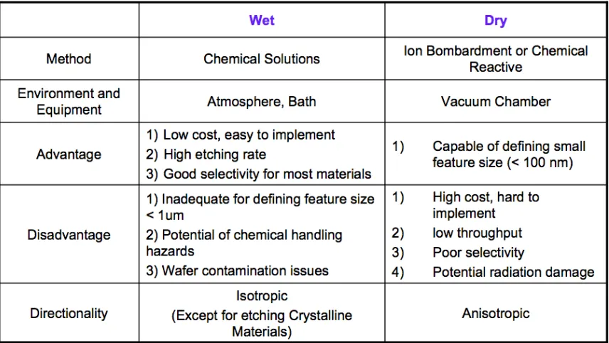
2.5. Comparison between Wet and Dry Etching
Table 2.1. Comparison between wet and dry etch [26].
2.5.1. Important Etch Terminology
Isotropic Etching: Etching rate is the same in both horizontal and vertical
direction
Anisotropic Etching: Etching rate is different in horizontal and vertical direction
Lateral Etch Ratio: Ratio of horizontal etch rate to
vertical etch rate components.
[image:52.612.113.541.105.346.2]
(2.9)
Bias:
The difference in lateral dimensions between the feature on mask and the actually
etched pattern. Smaller RL results in smaller bias. The etch bias problem can be mitigated
by using a compensation factor in mask dimensions. For example an etch bias of 0.5 m
can be counter balanced by using a 5.5 m etch mask to get 5 m transferred feature.
Under Cut and Over Etch:
As seen in figure 2.29, For RL =1 (left), over etching results in more vertical
profile but larger bias and severer undercutting, whereas for 0< RL <1 over etching results
[image:53.612.160.488.361.564.2]in poor CD control in thicker films.
Fig. 2.29. Pattern transfer for different lateral etch ratios (RL) during wet etch. [26].
Selectivity:
Selectivity is the ratio of etch rates of different materials in a etch process. The
selectivity with respect to mask material is denoted by Sfm and with respect to underlying
and
(2.10)
Degree of Anisotropy:
A = 1 - RL where, RL=0 represents isotropic etching and, RL=1 represents anisotropic etching
[image:54.612.235.435.258.522.2]Mask Erosion (Faceting): Film-Mask Etching Selectivity:
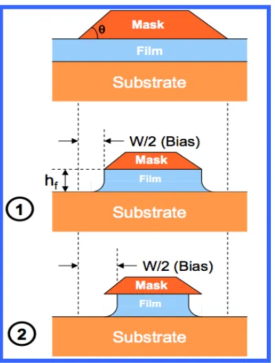
Fig. 2.30. The progression of the etched feature with finite mask etch rate (mask erosion). The CD loss is twice the bias width and is given by µ:¶[26].
As depicted in figure 2.30, the ratio of the total loss of linewidth (W) dimension of the
mask to film thickness (hf) is given by;
Case I: If film horizontal etch rate (rfh) < mask horizontal etch rate (rmh)
Mask lateral etch ratio,
(2.12)
Case II: Film horizontal etch rate (rfh) > mask horizontal etch rate (rmh)
(2.13)
Thus, it is extremely important to have a good etch mask for anisotropic etching.
Resist is most widely used as an etch mask, but, is not good for high aspect ratio etching
because it is readily attacked by the etch chemistries used. Many approaches have been
used to improve the etch resistance capabilities of resists such as hard baking the resists
at near glass transition temperatures. But, this leads to serious reflowing of resist owing
to higher temperatures leading to rounded-resist tops, which itself is problematic and may
FDXVH XQGXH LQFUHDVH LQ &'¶V GXH WR PDVN HURVLRQ DQG IDFHWLQJ LVVXHV GXULQJ HWFKLQJ
The corner of resist is always rounded even when the mask walls are vertical. These
corners etch faster and erode quickly than the other areas. Also, the sputter etch yield of
materials is a function of incident angle of the ions.
The corner-faceting is shown in figure 2.31. For example, the sputter etch rate of
resists is maximum at the incident angles of 600 as compared to normal ionic incidence.
Thus, the sloped sidewall of a mask may lead to sloped etching sidewalls, which may
further deteriorate due to increased electric field at the corners because of the applied
bias. The faceting can be controlled by an ideal or near-squared resist top profile. Other
techniques available for increasing the etch endurance of the resist mask are
UV-hardening and e-beam UV-hardening [28], but they are not feasible here at RIT due to special
tool requirements.
Loading and Micro-loading effects
The etch rates decrease with increase in etchable surface in chamber is termed as
loading effect. This effect is caused by gas phase etch species depletion by reaction with
material being etched. The loading effect is predominant in silicon etching in
fluorine-based chemistries because etching reactions dominate the loss of fluorine. However, in
bromine and chlorine based chemistries etch rates are less vulnerable to load size and
circuit topology conditions as the concentration of atoms in such plasmas are limited by
atom-atom recombination [29]. The loading effect is undesirable because it causes: a)
etch rate drop, b) loss of throughput and leads to process non-uniformities from
run-to-run and c) once the end point is achieved, the etchable area increases abruptly and causes
increased etch rate with just the sidewalls being exposed. This aggravates the
undercutting problem. Micro-loading effect accounts for slower etching of denser
features than isolated features (within wafer non-uniformities), and isolated lines etch
slower than trenches. This effect is even more severe from center to edge of the wafer.
and high surface area; b) allowing the removal rate by pumping to dominate by using
large gas flows and; c) by using an electrode made of material similar to one being etched
to reduce process dependence on wafer quantity.
2.5.2. Dry Etching
Figure 2.32 illustrates the sequence of events occurring during a plasma-assisted
etch process. The slowest process is the ultimate rate-determining step.
Fig. 2.32. Plasma etching mechanism with the sequence of processes.
I. Generation of etching species (Gas phase reactions)± The etching will not proceed
without any etch species. Reactive species (radicals and ions) are generated in the
plasma. Radicals cause chemical reaction and ions cause bombardment.
II. Surface Diffusion (Mass transport) ± Reactive species diffuse towards the surface
to be etched, the mechanics of getting to the surface can limit etch rates, aspect
ratio, undercutting and uniformity
IV. Chemical Reaction (Reaction rate controlling step)- Strong temperature
dependence (Arrhenius relationship)- affects the etch rate
V. Desorption ± The etch by-products needs to be highly volatile or the etch ceases
VI. Diffusion to bulk gas- May cause dilution of un-reacted etching species leading to
non-uniform etching
The ultimate goal of an etch process is to reproduce the features on the mask with
precision and possess following attributes:
1) High selectivity with respect to mask and underlying layer.
2) Suitably high throughput.
3) Etch uniformity; wafer to wafer, across wafer and over different runs.
4) The process should be safe and cause minimum substrate damage.
2.5.3. Reactive Ion Etching (RI E)
As seen in the figure 2.33, a typical RIE system consists of a vacuum chamber
and two parallel electrodes connected to a high frequency RF power supply (usually
13.56 MHz). The wafers are placed on a cathode plate that is grounded to electrically
isolate from the rest of the chamber. Gas enters the chamber through a showerhead, and
exits to the vacuum pump system through the bottom. The gas selection depends upon the
etch process. The pressure inside the chamber is maintained between a few mTorr - few
hundred mTorr to sustain the plasma. This can be achieved by tuning the gas flow rates
Fig.2.33. Schematic of a typical parallel plate RIE system [26].
Operation
Applying a strong radio frequency electromagnetic field to the wafer plate ignites
the plasma. The oscillating electric field ionizes the gas molecules by impact ionization,
stripping them of electrons, creating plasma. The electrons are accelerated up and down
in the chamber due to the E-field sometimes striking both the upper wall and the cathode.
However, the ions being much more heavier move relatively lesser in response to the
E-field. The electrons absorbed into the cathode leads to charge build up due to its DC
isolation. This build up leads to a negative self-dc bias on the cathode, of the order of few
hundred volts. Whereas, the plasma is always positive relative to grounded electrode due
to the higher concentration of positive ions compared to free electrons.
Under the influence of a large potential difference, positive ions tend to drift
toward the cathode causing collisions with the sample/wafer. These ions can react e- + C F
-material. The vertically directed reactive ions/ species, can produce near 90 degree etch
profiles, which contrast with the typically sloped wet etching profiles. The sheath
WKLFNQHVV LV RI WKH RUGHU RI µDebye OHQJWK¶and features smaller than this characteristic length can be etched directionally. The mean free path length must be greater than
chamber dimensions (i.e.low gas pressure) to prevent the reflection and re-deposition of sputtered species.
Parameter control in RI E process
Implementing an etch process that possesses the desired characteristics involves
control of the large number of parameters affecting that process. Figure 2.34 illustrates
some of the parameters that affect the gas-phase and the surface phase interactions. The
more macroscopic factors being pressure, power and the gas flow rates. In fact, the
macroscopic factors are coupled to the basic plasma parameters. A change in
macroscopic parameters may lead to complex interactions and alter two or more basic
parameters such as potential or temperature.
For example: gas flow, pumping speed and pressure are interrelated factors and
needs simultaneously fine tuning to control pressure. This makes the Dry-Etch process
development a profound challenge and demands a designed experimental approach.
Effect of Pressure and F requency
At pressures lower than ~ 50 - 100 mTorr, the sheath thickness and sheath
potential increases from 10s - 100s of volts. In this regime, plasma potential goes up and
ionic bombardment energy is precipitously increased with decreasing pressure. Finally, at
very high ionic energies and low gas pressure, physical sputtering dominates. However,
sputtering does not occur until ionic energy exceeds a material and ion-specific threshold
[29]. The similar effect is seen when frequency is lowered from around 5 MHz to
1MHz with gas pressures being in range of 100-100 mTorr. Thus, either low frequency or
low pressure can be used to induce anisotropy.
Effect of Temperature
Just like pressure, temperature has a profound influence on etching. For e.g. etch rate constant are Arrhenius function of temperature. Physisorption and diffusion are
sensitive to temperature which inturn can affect selectivity and anisotropy. High
temperatures (>1200) assist in anisotropic sidewalls.
Table 2.2 compares the different etching methods commonly employed in
Table 2.2. Dry etching spectrum with typical etching characteristics.
2.5.4. Dry Etch Gas Selection
Gas mixture of CF4 + O2 + N2 gives high Si3N4/ SiO2 etch selectivity, where N2
acts as diluent gas, improves heat transfer and forms active etch species [30] and CHF3 +
[image:62.612.107.543.111.335.2]O2 gives high SiO2/ Si selectivity and anisotropy [31].
Table 2.3. Typical etch chemistries and the byproduct of dry etching reactions. Types of Etching Gas/vapor Etching Plasma Etching Reactive ion
Etching Sputtering Etching
Methods Chemical Chemical Chemical & Physical (ion) Physical
Geometry Isotropic Isotropic Directional Directional
Selectivity Very High High Fair Low
Excitation Energy
None 10's to 100's of Watts
100's of Watts 100's to 1000's of Watts
Pressure High (760-1torr)
Medium (>100 mtorr)
Low Medium (10-100 mtorr)
Low (~10 mtorr)
Materials Etch Gas Etch Product
Silicon Cl2, CCl2F2 SiCl2, SiCl4
Si, SiO2, Si3N4
(Si3N4 etch rate > SiO2 E.R)
CF4 + H2, SF6, NF3,
CHF3 + O2
SiF4
(Low Si3N4/ SiO2 Selectivity)
High selectivity (~10:1) Si3N4/ SiO2 CF4 + O2 +N2
Aluminum BCl3, CCL4, SiCl4, Cl2 AlCl3, Al2Cl6
n-type doped Si etches faster (reaction rate increased by ~2.5 X) than P type doped Si
(reaction rate reduced by 0.8X) [32] in fluorine based feed gas system, while heavily
doped n-type Si and polysilicon in Cl atom plasmas etch 15-25 times faster than undoped
films.
2.5.5. Dry Etching Si/ SiO2 in Fluorine Based Gases and Plasmas
CF4 does not chemisorb on Si, and would not etch silicon in absence of plasma.
Etching is accomplished by creation of radical species (fluorine atoms) produced
by dissociation of CF4 molecules.
Etch Rate and Si/ SiO2 selectivity dependence on O2/ C F4 ratio
Insufficient F- atom concentration leads to a slower etch rate even with plasma.
However, with the addition of O2, F-atom concentration increases according to
reactions;
O + CF3 ÆCOF2 + F,
And, then O+COF2 ÆCO2 + 2F
Fig. 2.35. Normalized etch rate of Si and SiO2 versus the O2 concentration in CF4 ± O2 gas
[31].
As illustrated in figure 2.35, etch rate maximizes around 12% O2 and decreases at
higher O2 concentration because of dilution of F atom concentration by overly
abundant O2.
Etch Rate and SiO2/ Si selectivity dependence on H2/ C F4 ratio
H2 is a fluorine scavenger, i.e. reduces Fluorine to Carbon ratio (F/ C ratio),
thereby reducing F- atoms concentration by following reaction:
H+ + F+ e-ÆHF
[image:64.612.238.413.271.461.2]Addition of H2 increases SiO2/ Si etch selectivity tremendously. As seen in the
figure 2.36, at 40% of H2 concentration Si etch rate reduces to zero whereas SiO2
rate remains unaffected.
Fig. 2.36. The etch rate of resist, SiO2 and poly-Si in a RIE configuration versus H2
concentrations in CF4 - H2 feed gas system [31].
Increased etch selectivity involves two mechanisms;
1) Higher deposition of non-volatile (carbon like) residues on Si surface
terminates the etching of Si.
2) Lesser accumulation of residue on SiO2 surface than on Si surface: Carbon
combines with locally available O2 (available from the byproduct of the etch
Fluorine-to-Carbon Ratio (F/ C) model
Fig. 2.37. The boundary between etching and polymerization conditions influenced by F/ C ratio of reactive species and the applied bias [31].
Plasmas with F/ C ratio less than 4 (for e.g. CHF3 has F/ C ratio of 3) are known
as fluorine deficient plasmas and produce similar effect as if adding H2 to the etch
gas. Increasing F/ C ratio increases Si etch rates, and decreasing the F/ C ratios
lowers them.
Conversely, the addition of O2 increases the F/ C ratios, because the oxygen
consumes more carbon than F atoms. The feed gases emulating similar effect are
CO2, F2, and NO2.
Also illustrated in the figure 2.37, the boundary between polymerization and
etching varies with the applied bias. Higher bias allows etching to occur at lower
![Fig.2.6. CD variations as function of electron dose for gold structures plated in 400 nm and 150 nm resist [11]](https://thumb-us.123doks.com/thumbv2/123dok_us/115289.11031/27.612.235.411.73.222/fig-variations-function-electron-dose-structures-plated-resist.webp)
![Fig. 2.29. Pattern transfer for different lateral etch ratios (RL) during wet etch. [26]](https://thumb-us.123doks.com/thumbv2/123dok_us/115289.11031/53.612.160.488.361.564/fig-pattern-transfer-different-lateral-etch-ratios-etch.webp)
![Fig.2.33. Schematic of a typical parallel plate RIE system [26].](https://thumb-us.123doks.com/thumbv2/123dok_us/115289.11031/59.612.216.428.77.313/fig-schematic-typical-parallel-plate-rie.webp)