Rochester Institute of Technology
RIT Scholar Works
Theses
Thesis/Dissertation Collections
2-1-1994
VHDL modeling and design of an asynchronous
version of the MIPS R30000 microprocessor
Paul Fanelli
Follow this and additional works at:
http://scholarworks.rit.edu/theses
This Thesis is brought to you for free and open access by the Thesis/Dissertation Collections at RIT Scholar Works. It has been accepted for inclusion
in Theses by an authorized administrator of RIT Scholar Works. For more information, please contact
Recommended Citation
VHDL MODELING AND DESIGN OF AN
ASYNCHRONOUS VERSION OF THE MIPS
R3000 MICROPROCESSOR
by
Paul Fanelli
A Thesis Submitted
In
Partial Fulfillment of the
Requirements for the Degree of
MASTER OF SCIENCE
In
Computer Engineering
Approved by:
Graduate Advisor - Prof. George A. Brown
Department Chairman - Dr. Roy Czernikowski
Reader - Dr. Tony Chang
DEPARTMENT OF COMPUTER ENGINEERING
COLLEGE OF ENGINEERING
ROCHESTER INSTITUTE OF TECHNOLOGY
ROCHESTER, NEW YORK
THESIS RELEASE PERMISSION FORM
ROCHESTER INSTITUTE OF TECHNOLOGY
COLLEGE OF ENGINEERING
Title:
VHDL Modeling and Design of an Asynchronous Version of the MIPS R3000
Microprocessor.
I, Paul Fanelli, hereby deny pennission to the Wallace Memorial Library of RIT to
reproduce my thesis in whole or in part
_-ABSTRACT
The
goal of
this thesis
is
to
demonstrate
the
feasibility
of
converting
a synchronous
general
purpose
microprocessor
design
into
one
using
an
asynchronous
methodology.
This
thesis
is
one of
three
parts
that
details
the
entire
design
of an asynchronous
version
of
the
MIPS R3000
microprocessor.
The design
includes
the
main architectural
features
of
the
R3000:
the
5-stage
pipeline, the thirty-two
32-bit
register
bank,
and
the
32-bit
address
and
data
paths.
To limit
the
size
of
the
project, the
memory
and
coprocessor
are
excluded.
Therefore,
this
design
has implemented
the
entire set
of
instructions from
the
original synchronous
version with
the
exception of
the
coprocessor
support
instructions.
The
three
participants
in
this
project are
Paul
Fanelli,
Kevin
Johnson,
and
Scott
Siers.
Paul
Fanelli
developed
the
Very
High
Speed Integrated
Circuit Hardware
Description
Language
(VHDL)
models
for
the
processor.
Three
models,
behavioral,
dataflow,
and
structural,
were
constructed.
Kevin Johnson
designed
the
register
bank,
the
arithmetic
logic
unit,
and
the shifter,
including
schematic
diagrams
and
layouts.
Scott
Siers
designed
the
pipeline
stages, the multiplier/divider,
the
exception
handler,
and
the
completion
signal
generator,
including
schematic
diagrams
and
layout.
Each
of
the
TABLE
OF CONTENTS
ABSTRACT
iii
LIST
OF
FIGURES
vi
LIST OF
TABLES
x
GLOSSARY OF TERMS
xi
1.0
INTRODUCTION
1
2.0
CONCEPTS
6
2.1 ASYNCHRONOUS DESIGN
6
2.2 HANDSHAKING CONTROL CIRCUIT
7
2.3 VHDL
11
2.4 TOP DOWN DESIGN
12
2.5 DATATYPES
15
3.0
BEHAVIORAL
MODEL
17
3.1
INSTRUCTION FETCH
21
3.2 INSTRUCTION DECODE
23
3.3 INSTRUCTION EXECUTION
35
4.0
DATAFLOW MODEL
43
4.1 INSTRUCTION FETCH STAGE
46
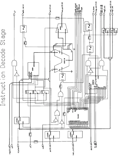
4.2 INSTRUCTION DECODE STAGE
50
4.3
ARITHMETIC LOGIC UNIT STAGE
66
4.4 MEMORY STAGE
68
4.5 WRITEBACK STAGE
72
5.0
STRUCTURAL
MODEL
79
5.1
GENERAL
PURPOSE
REGISTER BANK
79
5.2 ARITHMETIC
LOGIC UNIT BLOCK
83
6.0 RESULTS
102
6.1
TESTING PROCEDURE
102
6.2 DELAY TIMES
104
6.3
EXAMPLE
SIMULATIONS
107
6.4 PROCESSOR
SIMULATION TIMES
119
7.0 CONCLUSIONS
120
BIBLIOGRAPHY
124
APPENDIX A
-RLE
STRUCTURE
A-l
APPENDDC B
-BEHAVIORAL MODEL SOURCE CODE
B-l
APPENDIX
C
-DATAFLOW MODEL SOURCE CODE
C-l
APPENDDC D
-STRUCTURAL MODEL SOURCE CODE
D-l
APPEuNDIX E
-SUPPORT PROGRAMS
E-l
LIST
OF FIGURES
Figure 1-1. Test
Bench Block Diagram
3
Figure
2-1. HCC Architectural Organization
7
Figure
2-2.
HCC
Component
Block Diagram
8
Figure
2-3
.Handshaking
Control
Circuit
(HCC)
Schematic
Diagram
9
Figure
2-4.
HCC
Waveforms
10
Figure
3-1. Behavioral Model Test Bench
17
Figure
3-2.
The
Body
Outline
of
the
Processor Process
19
Figure
3-3.
Load Mode
20
Figure
3-4.
Run Mode
While-Loop
Shell
20
Figure
3-5.
Instruction Fetch
21
Figure 3-6.
Memory
Read
Procedure in Processor Process
22
Figure
3-7. R3000 Instruction Formats
23
Figure
3-8.
Extracting
the
Op-code from
the
Instruction
26
Figure 3-9. IF-ELSIF-ELSE Statement
used
for Instruction Decode
27
Figure 3-10. Special Instruction Branch
of
IF-ELSIF-ELSE
Statement
28
Figure
3-11.
Bcond Instruction Branch
of
IF-ELSIF-ELSE
Statement
29
Figure
3-12.
Jump
Instruction Branch
of
IF-ELSIF-ELSE
Statement
30
Figure
3-13.
Branch Instruction Branch
of
IF-ELSIF-ELSE Statement
31
Figure 3-14.
ALU
Immediate Instruction Branch
of
IF-ELSIF-ELSE
Statement
32
Figure 3-15. Load
and
Store Instruction Branch
of
IF-ELSIF-ELSE
Statement
33
Figure 3-16. Halt Instruction Branch
of
IF-ELSIF-ELSE
Statement
33
Figure 3-18. Reserved
Instruction
Branch
of
IF-ELSIF-ELSE
Statement
34
Figure 3-19.
The Shift Left Logical Instruction
36
Figure
3-20 The
Jump
Register Instruction
36
Figure 3-21.
The
Multiply
Instruction
37
Figure 3-22. The Add
Instruction
38
Figure
3-23.
The Branch
on
Less Than Zero Instruction
39
Figure
3-24.
The
Jump
Instruction...
40
Figure 3-25. The Branch
on
Equal Instruction
40
Figure
3-26.
The
Add Immediate Instruction
41
Figure 3-27. The Load Byte Instruction
42
Figure
4-1. Dataflow Model Test Bench
43
Figure
4-2.
Dataflow Model
CPU Component
45
Figure
4-3.
Schematic
of
IF
Stage
48
Figure
4-4.
Waveforms
of
IF
Stage
49
Figure
4-5. Instruction Decoder Component
50
Figure
4-6.
Schematic Diagram
of
ID
Stage
51
Figure
4-7.
Code Excerpt
of
the
ID
Stage Instruction Decoder Architecture
54
Figure
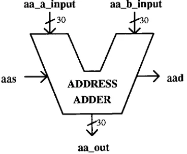
4-8. Address Adder
(AA)
Component
55
Figure
4-9.
Code Excerpt
of
the
Address Adder Architecture
56
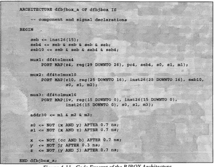
Figure
4-10.
Branch
and
Jump
(BJBOX)
Component
56
Figure 4-1
1. Code
Excerpt
of
the
BJBOX Architecture
57
Figure 4-12. Schematic Diagram
of
BJBOX
58
Figure
4-13.
Data
Dependency
Example
59
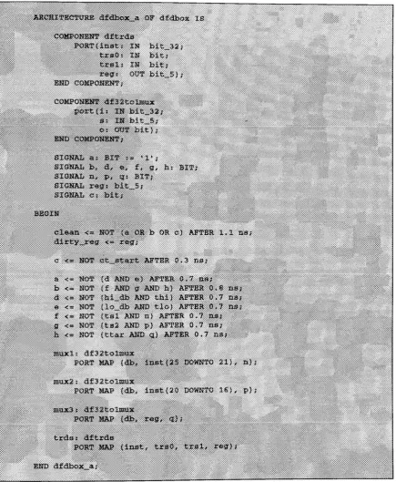
Figure 4-14. The
Dirty
Box
(DBOX)
Component
60
Figure 4-16.
VHDL
Code
of
the
TRDS
Architecture
61
Figure 4-17.
VHDL Code
of
the
DBOX
Architecture
63
Figure
4-18. Schematic
Diagram
of
TRDS
64
Figure
4-19. Schematic
Diagram
of
DBOX
65
Figure
4-20. ALU Stage
Block Diagram
67
Figure
4-21.
Schematic Diagram
of
MEM
Stage
69
Figure
4-22.
Code Excerpt
of
the
MU Architecture
70
Figure
4-23.
Code
Excerpt
of
the
SU Architecture
71
Figure 4-24. Schematic Diagram
of
WB Stage
73
Figure
4-25. BCU
Interfaces
to
IF, MEM,
and
Memory
74
Figure
4-26. Schematic Diagram
of
Bus Control
Unit
(BCU)
75
Figure
4-27.
BCU Waveforms
77
Figure
4-28. BCU FSM
State
Diagram
78
Figure 4-29. VHDL
Code
that
Implements
the
FSM
78
Figure 5-1. General Purpose Register Bank Component
79
Figure 5-2. VHDL
Code
of an
8-bit Wide Transmission Gate
80
Figure
5-3. VHDL Code
of an
8-bit Register
81
Figure
5-4. VHDL Code
of a
32-bit
Register
82
Figure
5-5. Arithmetic Logic Unit Block
(ALUB)
Diagram
84
Figure
5-6. Bus Control Block
(BCB)
Diagram
85
Figure
5-7.
The
A-Bus
Selector Component
86
Figure 5-8. The B-Bus Selector Component
88
Figure 5-9. The Bus Selection
Decoder
Component
89
Figure 5-10. Arithmetic Logic Unit
Component
(ALUC)
90
Figure 5-12. The
Overflow Block
Component
93
Figure 5-13. The Compare
Block
Component
94
Figure 5-14.
The Branch Control
Component
95
Figure 5-15.
The Shifter Unit
Component
96
Figure
5-16.
The Shifter
Unit Control Component
98
Figure
5-17.
The
Set
On Less Than
Unit Component
99
Figure
5-18.
The
Output Selector Component
100
Figure
6-
1
.
Example 1
-Arithmetic
Register Instruction Waveforms
1
09
Figure
6-2. Example 2
-Branch Instruction Waveforms
1 1 1
Figure
6-3.
Example 3
-Jump
Instruction Waveforms
113
Figure
6-4.
Example 4
-Load Instruction Waveforms
1 14
Figure
6-5.
Example
5
-Multiplication Instruction Waveforms
1
17
LIST
OF TABLES
Table
2-1. HCC Component Signal Names
and
Descriptions
8
Table
3-1. R3000
Instruction
Opcode Bit
Encoding
25
Table
4-1.
Instruction Decoder
Select
Lines
52
Table
4-2.
Bit
Encoding
to
Determine Destination Register
52
Table
4-3.
WB
Stage
Destination Register Bit
Encoding
Scheme
72
Table
5-1. ALUC
Operation
Encoding
90
Table
6-1. Gate
Delay
Times
105
Table
6-2.
Component
Delay
Times
107
GLOSSARY OF TERMS
AA
Address
Adder,
hardware
unit
that
calculates
the
address
of
next
instruction,
located
in
the
instruction decode
stage of pipeline
Accusim
Mentor
Graphics Corporation analog
circuit simulator
ADD8
Unit inside
the
ALU
stage
that
calculates
the
link
address
for branch
conditional
instructions
ALU
Arithmetic
Logic
Unit,
third
stage of
the
pipeline
ALUB
Arithmetic Logic Unit
Block,
one of
the
units
that
comprises
the
ALU
stage;
consists of
the
ALUC,
ALUC
decoder,
shifter,
shifter
control,
branch
control,
etc.
ALUC
Arithmetic
Logic
Unit
Component,
unit
that
performs
addition,
subtraction,
and
logical
computations
bcond
Branch
Conditional
group
of
instructions
BCB
Bus Control
Block,
unit
inside
the
ALUB
that
controls what
gets placed
on
the
A
and
B
busses in
the
ALU
stage
BCU
Bus Control
Unit,
unit
that
controls
which
stage
(IF
or
MEM)
is
granted
access
to
the
address and
data busses
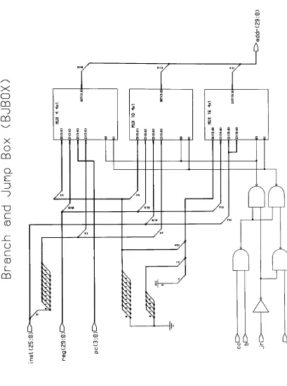
BJBOX
Branch
and
Jump
Box,
unit
inside
the
ID
stage
that
controls what gets
sent
to the
AA
bton
Bits-to-Natural
function,
converts
bits
to
natural
numbers
CMOS
Complementary
Metal
Oxide Semiconductor
CPU
Central
Processing
Unit
current_inst
Variable
that
holds
the
current
instruction
DBOX
Dirty
Box,
unit
inside
the
ID
stage
that
handles
data
dependencies
DOD
Department
of
Defense
ea
Variable
that
holds
the
effective
address,
used
to
calculate effective
address
of
load
and store
instructions
EH
Exception
Handler,
unit
that
handles
exceptions
from
the
IF, ID,
ALU,
and
MEM
stages and generates an
interrupt
vector
that
is
sent
to the
IF
FLOW
Reorders
a program
that
contains
branch
and
jump
instructions
to
follow
the
program
flow.
FSM
Finite
State Machine
funct
Function
field
that
holds
the
minor operation
code
used
for instruction
decoding
GPR
General Purpose Register
HCC
Handshaking
Control
Circuit
ibo
Immediate
or
base-offset,
one of
the
output signals of
the
instruction
decoder
in
the
ID
stage
that
goes
high
either
for
an
immediate
instruction
or
for
an
instruction
that
needs a
base-offset
calculation
ID
Instruction
Decode,
second
stage of pipeline
IE
Instruction Execution
IF
Instruction
Fetch,
first
stage of pipeline
immed
Field
that
holds
the
immediate
value used
for instruction
decoding
LSB
Least Significant Bit
MASS
MIPS
Assembler,
program written
to
convert
MIPS assembly
code
into
machine code
MDU
Multiplier/Divider
Unit
MEM
Memory,
fourth
stage
of
pipeline
MERA
MIPS Expected Results
Assembler,
program written
to
help
generate an
MIPS
MPP
MSB
MU
ns
offset
op
opcode
PC
pc_reg
R3000
rd
RISC
rs
rt
shamt
special
SU
target
Name
of
company
that
designed, developed,
and
built
the
R3000
microprocessor,
also stands
for Millions
of
Instructions Per Second
which
is
a
processor speed
rating
MIPS
Preprocessor,
program written
to
load
processor with
test
programs
Most
Significant
Bit
Mask
Unit,
unit
inside
the
MEM
stage
that
determines
the
length
of
the
requested
data
and whether
the
data is
sign or
zero-extended
Nanoseconds
Field
that
holds
the
offset
value used
for instruction
decoding
Field
that
holds
the
major
operation code
used
for instruction
decoding
Operation Code
Program
Counter
Variable
that
holds
the
program counter
value
Model
number
of
processor
this thesis
is modeling
Destination
register
field
used
for instruction
decoding
Reduced
Instruction
Set Computer
Source
register
field
used
for instruction
decoding
Target
register
field
used
for instruction
decoding
Field
that
holds
the
shift
amount
Special
Instructions,
name
of
group
of
MIPS instructions
Shift
Unit,
unit
inside
the
MEM
stage
that
shifts
data
when
it is
not
aligned on a
word
boundary
TRDS
Target Register
Dirty
Select,
unit
that
selects
which
register will
be
set
dirty
vbt
Valid Byte
Tag,
this
signal
is
generated
by
the decoder
inside
the
MEM
stage and
is
used
by
the
GPR bank in
the
ALU
stage;
it
specifies
which
bytes
of
data
are valid and can
be
written
back
to
a register
VHDL
VHSIC Hardware Description Language
VHSIC
Very
High
Speed
Integrated
Circuit
VLSI
Very
Large
Scale
Integration
1.0
INTRODUCTION
This
thesis
is
one
of
three
parts
encompassing
the
modeling,
design,
and
implementation
of
an
asynchronous
microprocessor.
This
project
was
performed
cooperatively
by
Scott
Siers,
Kevin
Johnson,
and
this
author.
The
project
has been
divided
so
that
each part
forms
a separate
master's
thesis.
This
paper
discusses
the
Very
High
Speed
Integrated
Circuit Hardware Description
Language
(VHDL)
modeling
of
this
processor.
The
asynchronous
processor uses most of
the
R3000's instruction
set
and
architectural
features
but
differs
in
implementation.
Three
models,
behavioral,
dataflow,
and
structural,
are constructed.
The behavioral
model
describes
the
functionality
of
the
R3000
without regard
to
implementation.
The dataflow
model
represents
the
pipeline
of
the
processor.
It
models
the
data
flowing
through the
pipeline stages.
The
structural
model represents
the
processor at
the
gate or structural
level.
The
dataflow
and structural
model
delay
times
were
back
annotated
from
circuit simulation runs.
Each
model
is
tested
using
a
VHDL
test
bench
to
verify
correct operation.
Kevin Johnson
and
Scott
Siers
were
responsible
for
the
Very
Large
Scale Integration
(VLSI)
design
and
implementation.
Kevin Johnson
designed
the
register
bank,
the
arithmetic
logic
unit
(ALU),
and
the
shifter.
Scott Siers designed
the
bus
control
logic,
the
multiplier/divider
unit
(MDU),
and
the
pipeline
structure.
This
author
also
participated
in
the
design
of
the
asynchronous
processor
from
a
modeling
perspective.
The
hardware
designs
were
changed
or
completely
redone
depending
upon
the
results of
the
VHDL
modeling.
The
main purpose of
this
project
was
to
investigate
the
feasibility
of
converting
an
existing
synchronous
processor
design
to
an
asynchronous
design. The
MIPS R3000
was
chosen
for
this task
for
numerous
reasons.
The R3000 has
the
best
combination
of
instruction
set
size,
architectural
features,
and
system
complexity
to
fully
exploit
the
differences between
synchronous and
asynchronous
design.
The R3000
was one of
the
and
elegant architecture.
The
number
of
instructions
is
minimal
and
there
are
only
three
addressing
modes.
For
a
32-bit
machine
it has
a small architecture and
hence
makes an
ideal
processor
for
thesis
work.
There is
an
abundance
of
literature
written
on
the
MIPS
R3000.
For example,
the
paper written
by
Asada, Okura,
and
Cho
in 1992
[1]
discusses
the
design
of an
asynchronous
implementation
of
the
MIPS data
path.
Another
paper
by
Ginosar
and
Michell
[2]
discusses converting
the
MIPS
pipeline
using
an
asynchronous
design
methodology.
Also,
the
book MIPS RISC Architecture
[3]
gives
extremely
low-level
details
of
the
synchronous
version of
the
processor.
These features
make
the
R3000
an
ideal
processor
to
model.
The
MIPS
R3000
is
a general purpose microprocessor
that
includes
a
32-bit data
path with
thirty-two
32-bit
general purpose registers.
The R3000
has
a
5-stage
pipeline.
The
five
stages are
instruction fetch
(IF),
instruction decode
(ID),
arithmetic
logic
unit
(ALU),
memory
(MEM),
and register
writeback
(WB). The
three
main
addressing
modes
are
register,
immediate,
and
jump.
The R3000
is
a reduced
instruction
set computer
(RISC).
One
characteristic of a
RISC based
architecture
is
that
it is
a register
based
design.
The
processor
only
works
on
data
contained
in
the
registers.
The
order
of
operations
is
that
data
is
loaded from
memory into
the registers, the
processor
works
on
the
data
in
the registers, the
result
is
stored
back
into
a
register,
and
finally
the
result
is
put
back
into
memory.
The
advantage of
this
architecture
is
that the
instruction
set
is
smaller
(reduced)
and
consists
of
simpler
instructions.
This
allows
the
cycle
time
for
each
instruction
to
be
short.
All
of
the
R3000's instructions
are
32 bits in length.
This is
another
advantage
of
RISC
machines.
The complexity
of
the
instruction
decoder
is
minimal
and
the
instruction
set size
is
limited.
Before
any
modeling
was
done,
certain
issues had
to
be
considered.
What
architectural
features
were
to
be
modeled?
Which instructions
were
to
be
modeled?
How
many
specific
models
should
be designed
and at
what
level
of
detail?
During
preliminary
R3000
would
be
modeled:
the
5-stage
pipeline,
the thirty-two
32-bit
register
bank,
the
hi/lo
registers,
and
the
32-bit
address
and
data
paths.
The
features
that
would
be left
out
are
the
coprocessor
and coprocessor
support, the
cache
for
memory
and
instruction
fetch,
and
the
memory
management.
Since it
was
decided
that
memory
would
not
be
modeled,
memory
management
would
not
be
implemented.
The
coprocessor
and
memory
management
instructions
were
left
out.
Due
to these
architectural
decisions
and
to
limit
the
size
of
this
thesis,
the
asynchronous
processor
instruction
set was reduced.
The VHDL
modeling
in
this
thesis
consists
of
the
following
three
models:
behavioral, dataflow,
and
structural.
All
models consist of
three
modules:
memory,
central
processing
unit
(CPU),
and compare.
These
three
modules
when put
together
with
the test
program and
the
expected results
file
create a complete
test
bench.
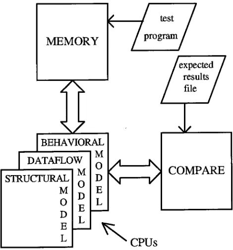
Figure 1-1
shows
the test
bench
setup.
Each
model
will
use
the
test
bench along
with
test
programs
to
verify
correct operation.
The memory
and compare modules
are
relatively
similar
for
all
three
models.
The
memory
module
is
used
as
the
main
memory
storage
for
the
BEHAVIORuAL
M
DATAFLOW
M
STRUCTURAL
M
O
D
E
L
?c
K
expected
results
file
V
COMPARE
[image:18.520.144.379.411.663.2]CPUs
processor and
holds
the
test
program used
in
the test
bench.
The
compare module
is
used
to test the
state
of
the
processor after each
instruction is
executed and
holds
the
expected
results
file. The CPU
module
corresponds
to
one of
the three
models.
Software
was
written
for
this thesis to
assist
in
testing
the
models.
An
assembler,
called
MIPS
Assembler
(MASS),
was
written
to
convert
MIPS assembly
code
into
machine code
that the
models
can understand.
Also,
an expected results
program
was
written.
This program,
called
MIPS Expected
Results
Assembler
(MERA),
allows
the
user
to
input
the
expected results
data
into
a
file.
This file is loaded into
the
compare
module and
is
tested
against
the
state of
the
model after each
instruction
is
executed.
Another
program
was
written
for branch
and
jump
instructions.
This
program,
called
FLOW,
takes
a program
that
contains
branch
and
jump
instructions
and reorders
the
instructions
to
follow
the
program
flow.
The last
program
is
called
MIPS Preprocessor
(MPP).
This
program
takes the
files
created
by
MASS
and
MERA
and copies
them
into
two
files
that
are used
by
the
models.
These
two
files,
"machine"and
"expected",
are
loaded
by
the
memory
and compare
modules,
respectively.
Six
test
programs
were written
for
the
models.
Each
of
these
tests
correspond
to
a
set of
instructions. The
program
"ai.test"
tests
immediate
arithmetic
instructions,
"ar.test"tests
register arithmetic
instructions.
The
third
program,
"jb.test",
is
used
for
jump
and
branch instructions. The
program
"ls.test"
is
used
to test
load
and store
instructions. The
fifth
test,
"md.test",
checks
the
multiplication
and
division instructions along
with
the
move
to
and
from
the
hi/lo
registers.
The last
test
file, "s.test",
is
used
for
the
shift
instructions.
The
software
tools
used
in
this
project
are
from Mentor Graphics Corporation
and
run
on
HP/Apollo Workstations.
Five
software
tools
were
used:
Design
Architect,
System-
1076
(VHDL)
editor and
compiler,
Quicksim
II, Accusim,
and
IC Station. Design
Architect
is
a schematic capture
tool.
The VHDL
editor
and compiler
is incorporated into
embedded
into Quicksim
II.
Accusim
is
the
analog
circuit
simulator.
Finally,
the
mask
2.0
CONCEPTS
One
major
feature
of
synchronous
design is
the
use of a global
clock.
The very
nature of
synchronous
design
is
to
control all
events
based
on
this
clock.
Multiple
events
can
happen but
they
will
not
be
triggered
until
the
next clock pulse.
The
order of events
is
of no
concern.
On
the
other
hand,
asynchronous
design
avoids
the
use
of a global clock.
Therefore,
there
is
no
convenient
way
to
synchronize
events.
Here,
the
order of events
is
very
important.
A
controller can
be
used
between logic blocks
as
a communication
device.
The
controller
uses
start
and
done
signals as
handshake
signals.
When
one
logic
block
is
finished,
it
sends
the
controller a
done
signal.
The
controller can now send
the
next
logic
block
a start signal.
With
synchronous
design,
the
logic blocks
can
be
tuned to
start at a certain
time
based
on
the
clock phase.
However,
the
exact
time
at
which
a
specific event starts or ends
is
not
known in
asynchronous
design. This
is
why
a controller
is
needed.
It
coordinates
the
timing
of
events
through
the
use of
handshaking
signals.
2.1
ASYNCHRONOUS
DESIGN
An
asynchronous
design
approach
was chosen over a synchronous one
for many
reasons.
As
transistor
sizes
in VLSI
keep
getting
smaller, the
major
drawbacks
to
synchronous
design become
more
apparent
and
difficult
to
tolerate.
Two
major
disadvantages
are
the
skew associated
with
a
global
clock and
the
increasing
line
delay
that
occurs
when
a signal
is
routed across a
VLSI
chip.
One
of
the
major
design
goals
in
synchronous
design
is
to
increase
the
performance of
the
processor
by
reducing
the
clock
period.
However,
as
the
reduction
in
scale of
VLSI
systems
continues,
more and more of
the
clock period
is
used
to
account
for
clock skew.
Global
clock
lines become
more
sensitive
to
loading
and
it
becomes
increasingly
difficult
to
keep
the
various
clock
line
circuit
design
was
the
transistor
gate.
Today,
the
line
delay
in
signal
routing is
a
major
concern.
To
obtain
substantial
increases
in performance,
new
architectures
will
have
to
be
used
to
reduce
the
need
for
long
metal
lines.
Circuit
modules
will
have
to
be linked only
by
local
interconnections
and
the
modules
will
then
communicate
via
self-timed
handshaking
schemes.
The
asynchronous
design
that
eliminates
the
global
clock
and
reduces
the
need and effects of
long
signal
lines
is
an attractive solution
in
modern
VLSI
implementation.
2.2
HANDSHAKING CONTROL CIRCUIT
The
handshaking
control circuit
(HCC)
represents
the
control
flow
mechanism
for
the
asynchronous
machine.
Every
major
logic block in
the
design has
an
HCC
associated
with
it.
The HCC
synchronizes
the
events
among
the
major
logic blocks.
The
HCC
coordinates
control
information from its
own
logic block
and
from
other
HCCs in
the
design.
Figure 2-1
shows
the
HCC
architectural organization.
The
major
logic blocks
shown
in
the
diagram
correspond
to the
five
pipeline stages of
the
processor.
An HCC
is
dependent
on
the
previous
and
the
next
HCC.
The
HCCs
on
the
ends
of
the
pipeline
are
init
only
dependent
on
its
one neighbor.
For example,
the
ALU HCC is dependent
on
the
ID
and
MEM
HCCs.
The.
ALU
stage
cannot
begin
operation until
the
ID
stage
is finished
and
the
MEM
stage
has
latched
the
previous
data from
the
ALU
stage.
The HCC
component
block
diagram
is
shown
in Figure 2-2. The
signal names and
their
descriptions
are shown
in
Table
2-1.
Figure
2-2.
HCC
Component
Block Diagram
SIGNAL NAME
DESCRIPTION
init
Initializes
the
HCC
ok(n-l)
Previous
stage
has
completed
its
operation
aout
Acknowledgment
to
previous
stage
that
data has been latched
rout
Start
signal
to
logic block
ready
Done
signal
from logic block
ok(n)
Signals
next stage
that
present stage
is
completed
ain
Acknowledgment from
next
stage
that
data has been latched
Table 2-1. HCC Component Signal Names
and
Descriptions
The HCC
schematic circuit
diagram
is
shown
in Figure 2-3
and
its
waveforms are
shown
in
Figure 2-4.
The
operation
of
the
HCC
is
as
follows.
The init
signal
is
used
to
initialize
the
HCC
and acts
like
a reset.
The
ok(n-l)
signal
is
the
start signal
for
the
HCC.
cj
CJ
o
c
CJ
o
c
o
CJ
CD
jv:
CD
_CI
CO
n^
CZ
CO
AAA
~3>
<Z
-j*-^^
~TJ
"CO
CO
CZ
CD
' ~
a
L-o
cn
cn
*t-cn
co
cn
cn
LO
cn
cn
cn
cn
.cn
cn
co
cn
to CXJ
cn
cn
/N
/N
/|\
A\
/J\
ff\
ok(n-l)
|
rout
|
ok(n)
|
aout
ready
ain
previous stage
has
valid
data. The
HCC
sends
the
acknowledgment
signal aout
high
when
rout
and
ready
are
both
low.
When
aout
is high
and
ain
is
low,
rout
goes
high,
rout
is
the
start signal
to the
HCCs
logic
block.
The
HCC
now waits
for
the
completion of
the
logic
block. This is
signified
by
the
ready line
going high. Once
ready
is
high,
the
HCC
sends
ok(n)
low.
This
signals
to the
next
HCC
that the
logic
block
has
valid
data.
The HCC
now waits
for
ain
to
go
high
which
is
an
acknowledgment
from
the
next
HCC.
ain
going
high
causes
rout
to
go
low
and
ok(n) to
go
high.
When
rout
goes
low,
ready
goes
low.
The
cycle
then
repeats
itself.
2.3 VHDL
VHDL
stands
for VHSIC
Hardware
Description
Language.
VHSIC
stands
for
Very
High
Speed Integrated Circuit.
The
Department
of
Defense
(DOD)
initiated
the
VHSIC
program.
The DOD
also
initiated
VHDL
to
create
a
hardware description
language
that
all
VHSIC
contractors
could use
to
specify
their
designs.
More
importantly,
this
would
allow
designs
to
be
transferred
from
one
company
to
another and
be
totally
independent
of
the tools
and
the
platforms
they
run on.
VHDL is
a
high level language.
High level
constructs are
important
for design
specification
(behavioral model)
and
testing.
VHDL
allows
the
user
to
concentrate on
the
behavioral
aspects of
the
design
and
forget
the
low level
details
during
the
beginning
stages
of
design.
VHDL
is
an
IEEE
standard
formalized in
specification
1076-1987
and
updated
in
specification
1076-1992.
Writing
in VHDL
allows
the
user
to
port
the
source
code
over
to
another
hardware
platform
with
ease.
All
that
needs
to
be
done is
to
recompile
the
source code on
the
new
platform
and
to
run
the
new platform's
simulator.
VHDL
is
a
programming
language
that
can
simulate
concurrent events.
This
concept
of
delta
delay,
which
is
an
infinitesimally
small
delay,
to
order
events
that
occur at
the
same simulation
time.
VHDL
software
tools
incorporate
a
simulator
to test the
design,
and
a
test
bench
can
be
used
to
simplify
the
testing
process.
Also,
VHDL has
packages
specifically
designed
to
model
hardware
at
different
stages of
design.
2.4 TOP
DOWN DESIGN
Top
down design
is
a popular
design
methodology.
It
guides
a
design
from
a
high
level
to
a
low level
of abstraction.
The
system's
functionality
is
described
at a
high level
of
abstraction.
Implementation
of
this
functionality
is
not an
issue
at
this
level.
On
the
contrary, the
system's
low level
details
are
only
considered at a
low level
of abstraction.
The
low level describes
the
gate
level implementation. As
the
design
progresses
from
one
level
of
abstraction
to the next,
functionality
of
the
design is
completed and set at
the
higher
levels
and
then
the
implementation
of
this
functionality
is
created at
the
lower
levels.
This
thesis
uses
this
concept
by
using
the three
different
models.
Each
model
is
another
level
of abstraction.
A behavioral
model
is
a
model
that
describes
the
behavior
of
the
hardware entity
under
test.
An entity
is
a
hardware
unit
that
can
be
as simple as a gate or as
complex
as
an
entire
electronic system.
A behavioral
model
does
not
explicitly
specify
the
structure
of
the
entity but
specifies
its
functionality.
Another way
of
looking
at
the
behavioral
style of
modeling is
the
well
known "black
box"approach.
The hardware
unit
is
described in
terms
of
its
input-output mapping
without
specifying
the
model's
technology,
components,
or
dataflow.
A behavioral
model projects a
very high level
of
abstraction.
At
the
first
stages of
design,
the
behavioral
model relieves
the
user
of
the
low-level details
of
the
design
and
behavior
of
the
system
in
question.
Overall,
the
behavioral
model provides
a means
to
better
understand
the
functionality
of
the
entity.
Finally,
due
to
the
high level
of
abstraction,
the
behavioral
model
executes
much
faster
than
other
modeling
schemes.
This
is
advantageous
at
the
beginning
stages
of a
design
when
many
simulations need
to
be
done.
The
behavioral modeling
technique
was used
to
model
the
functionality
of
the
R3000
without regard
to
hardware implementation.
The behavioral
model
was used
to
understand
the
operation of
every instruction
that
was
implemented. The
entire
behavioral
model
is actually
one
VHDL
PROCESS
statement.
All instructions in
a
PROCESS
statement are executed
sequentially.
Therefore,
the
pipeline was modeled
in
a
sequential
fashion.
An
instruction is
fetched, decoded,
executed, stored,
and
tested
all
within
one
cycle of
the
PROCESS
statement.
The
next
instruction
is
not
worked
on
until
the
first
instruction
is finished.
The data
type
used
in
this
model
is
the
BIT VECTOR. This
choice
is discussed in
section
2.4. The
computation
instructions
are
implemented using functions
and procedures since
this
model
is
only
concerned
with
the
operation of
the
processor
and
not on
how it is
implemented.
These
functions
and procedures
are
located in
a
VHDL
PACKAGE.
A dataflow
model
describes
the
behavior
of
the
hardware entity just like
the
behavioral
model
but
in
more
detail.
Dataflow modeling involves
some
implementation
details
since
it
is
concerned
with
the
flow
of
data from
one part
to
another.
The dataflow
model starts
to
break
the
functionality
of
the
behavioral
model
down
into
compartments.
An
example of
this
is
the
breakdown
of
the
pipeline.
Each
stage of
the
pipeline performs
a
different
function. The dataflow
model specifies
how
the
data
will
flow from
one section
to
another.
Dataflow modeling
is
similar
to behavioral
modeling
since
there
are no gates
to
specify
low level
implementation,
but
it
is
also
similar
to
structural
modeling because
of
The
dataflow
model
uses
the
same
data
types
and
package
of
declarations, functions,
and
procedures
as
the
behavioral
model.
This
was
done
to
simplify
the
model.
The
main
focus
of
attention
was
to
get
the
pipeline
stages
talking
to
each
other and
to
assure
that
each
stage
was
decoding
and
working
on
the
proper
instruction.
Also,
to
keep
the
dataflow
model
simple,
only
two
logic
states
(0
and
1)
were used
to
describe
and simulate
the
model.
The
dataflow
model
provided
the
next
level
of abstraction
by
modeling
the
pipeline
stages concurrently.
This
model
is
used
to
design
the
handshaking
interface
protocol
between
the
pipeline stages.
The
main
objective
of
this
model was
to
establish proper and
efficient communication
between
the
pipeline
stages.
A
rough protocol would
be designed
and
then tested
using
the
dataflow
model.
Using
the
simulation waveform
outputs
of
the
model,
the
protocol
was
modified
to
improve
the
design.
Also,
design
errors
were
corrected
using
the
dataflow
output waveforms.
This
continued
throughout the
entire
design
cycle of
the
asynchronous processor.
The
dataflow
model
is
largely
a
hierarchical
structure of
dataflow
components.
The
top
level
component
is
the
CPU.
The CPU
is
then
broken up
into
eight unique
components:
the
five
pipeline
stages, the
HCC,
the
bus
controller
(BC),
and
the
exception
handler (EH).
Each
stage
of
the
pipeline
has
an
HCC
associated
with
it.
Each
of
these
components
are
made
of other
smaller
components
and
primitives.
Examples
of
the
primitives
are
multiplexers,
latches,
and edge
detectors.
The
components
were used
to
speed
up
the
model
building
process.
When
a
particular
component
is
needed, the
proper
code
is
called
through
use of
the
VHDL
COMPONENT instantiation
and
PORT MAP
statements.
The
original
dataflow
model
was
constructed
using
arbitrary
delay
times
just
to
get
the
model
working.
Back
annotation was
used
once
the
model was
completed,
tested,
and
verified
for
correct
operation.
The
new
delay
times
were
obtained
from Accusim
These
simulations
were performed and
discussed
in
Scott
Siers'thesis
and
Kevin Johnson's
thesis
"Design
and
Implementation
of an
Asynchronous
Version
of
the
MIPS R3000
Microprocessor"[10,19].
The
structural
model
represents
the
processor
at
its
gate or structural
level. This
is
the
lowest
form
of abstraction.
It
is
the
lowest
and most
detailed level
of
description. The
structural model uses a set of
components connected
by
signals.
With
the
structural
model, the
behavior
of
the
entity is
not
apparent
from
the
model.
This
is
unlike
the
behavioral
model where
the
behavior
or
functionality
is readily
apparent.
Component
instantiation
is
the
major
VHDL
device
that
facilitates
a structural or gate
level
nature.
2.5 DATATYPES
Originally,
integers
were chosen as
the
main
modeling data
type.
However,
this
presented
some
problems.
The
representation of
data
by
integers
appears
to
be ideal but
instructions
need a more robust
data
type.
Different
pieces of
the
instruction
represent
different
aspects and conditions of
the
computer.
An instruction
holds
operation,
register
operand,
and
memory
address
information.
Also,
depending
on
the
addressing
mode,
an
instruction holds
different
types
and amounts
of
information.
A
composite
type
called a
record
was
considered
in
order
to
hold
all
the
different
fields
of
information
contained
in
an
instruction.
However,
Mentor
Graphic's
version
of
VHDL
now
in
use
(version
8.1)
does
not support records.
At
this
time,
a
decision
was
made
to
use a
data
type
called a
bit
vector.
Bit
vectors
are
ideal
to
use
because
they
represent
the
language
that the
computer understands.
Bit
vectors can
be
manipulated
using
two
methods.
Using
the
first
method, the
bit
vector
is
converted
to
an
integer,
the
integer
is
operated
on,
and
then
the
integer
is
converted
back
second
method
is
to
manipulate
the
individual
bits.
These bit
manipulations are
handled
by
procedures and
functions.
An
example of
this
is adding
two
bit
vectors
together.
The
two
bit
vectors
are
passed
to the
overloaded
"+"function.
The
"+"function
adds
the
individual
bits
together
and
returns a
bit
vector
result.
These
specialized
functions
add
3.0
BEHAVIORAL
MODEL
The behavioral
model
is
an
instantiated
component.
The
name of
the
model
is
CPU,
since
the
central
processing
unit
is
the
main
part
of
the
MIPS R3000
that
is
modeled.
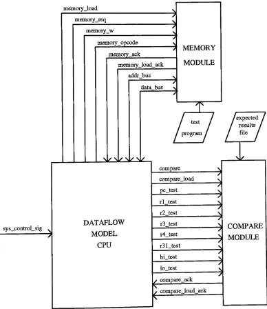
This CPU
component
is
part of a
test
bench
shown
in Figure 3-1.
The
other
two
components
of
the test
bench
are
the
memory
and compare modules.
The
memory
module
is
used
as main
memory
storage
for
the
processor.
It
is
accessed
by
six
interface
signals.
The
memory
control
signals, mem_control_sig
and
mem_control_sig
sys_control_sig
addr
bus
addr
bus lo
"}
mem_ack_sig
mem_exception_sig
data bus
\I/\I/mV
BEHAVIORAL
MODEL
CPU
MEMORY
MODULE
/"^
compare_control_sig
^
pc
^
rl
r2
r3
"}
r4
r31
hi
lo
compare_ack_sig
COMPARE
mem_ack_sig,
provide
a
fully
interlocked
handshaking
protocol
between
the
CPU
component
and
the
memory
component.
The
address
bus is
broken
into
two
separate
signals:
addrjbus and
addr_bus_lo.
Addrjbus
provides
the
upper
30 bits (bits 2
through
31)
of
the
32
bit
address
bus,
which
accesses
a word of
memory
(a
word
of
memory is
32
bits
wide).
Addrjbusjo
provides
the
lower
two
bits
(bits
0
and
1)
of
the
address
bus,
which
accesses a
byte
of
memory
(a
byte
of
memory is 8
bits
wide).
The
datajbus
is
a
32-bit
bi-directional bus.
It
is
used
to transfer
data between
the
CPU
and
the
memory
module.
Finally,
the
exception control
signal, mem_exception_sig,
is
activated
when
a
memory
exception occurs.
The
compare
module
tests the
state
of
the
processor
after each
instruction
is
executed.
It
is
accessed
by
ten
interface
signals.
The
compare
control
signals,
compare
_control_sig
and
compare_ack_sig,
provide
the
handshaking
between
the
CPU
and
the
compare module.
The
pc
signal monitors
the
CPU
program
counter.
Signals
rl,
r2,
r3, r4,
and
r31
monitor
the
contents of
the
specified registers.
The
hi
and
lo
signals
monitor
the
multiplication
and
division
storage
registers.
The CPU
module
or component uses a
VHDL PROCESS
to
model
the
processor.
A PROCESS
statement
is
a
collection
of
sequential
statements
that
describe
the
functionality
or
behavior
of a
portion
of
an
ENTITY.
A PROCESS is
first
entered
during
the
initialization
phase of
a
simulation.
During
this
initialization,
it
continues
to
execute
until
it
suspends
due
to
an
explicit
WATT
statement
or
an
implicit WATT
due
to
a
sensitivity
list.
Also,
once a
PROCESS
is
entered,
it
is
never exited.
It
is
always
in
one of
two
states:
active
or
suspended.
A PROCESS is
active
when
it is
executing
and
suspended when
it is
waiting for
a
certain
event
to
occur.
A PROCESS
is
sensitive
to
signals
in
a
sensitivity list.
If
an event occurs on
any
one
or
more
of
the
signals
in
the
sensitivity
list,
the
PROCESS
is
executed.
The
statements
in
the
PROCESS
are
executed
in
a
sequential
fashion.
It
suspends
after
the
sensitivity
list.
A WATT
statement
can
be
used
in
place
of a
sensitivity list.
A
PROCESS
executes
until
a
WATT
statement
is
reached.
The PROCESS
is
suspended
until
an event
occurs
on
the
signal
in
the
WAIT
statement.
The
body
outline of
the
PROCESS
used
in
this
model
is
shown
in Figure 3-2. It is
sensitive
to the
sys_control_sig
signal
using
a
WATT
statement.
The
process
is
broken
down,
using
a
VHDL CASE statement,
into
four
sections each
corresponding
to the
four
modes of operation:
stop,
reset,
load,
and
run.
processor*
PROCESS
--process
declarations
BEGIN
WAIT
ON
sys_control_Bigj
CASE
ays_control_sig
IS
stop
=>
WHEN
reset
=>WHEN
load
=>WHBS
run
->E8D
CASE;
END
PROCESS
processor.
Figure
3-2. The
Body
Outline of
the
Processor
Process
The load
mode,
shown
in Figure
3-3,
is
part of
the
system
initialization,
load
sends
signals
to the
memory
and
compare
components
to
load
the
system
programs.
More
precisely, the
load
mode
initiates handshake
signals
with
the
memory
and compare
components.
It
sends
the
load
signal
to the
memory
component via
mem_control_sig
and
to the
compare component via
compare
When
both
components are
finished
loading
their
respective
programs,
they
send
back
their
acknowledgment
signals.
A
reset
WHEN
load
=>run_mode_flag
:=no;
meH_control_flig
<-
load
AF7BR
delay
WAIT UNTIL
mem_ack_sig
=yes;
mem_cont.rol_sig
<=reset
AFTER
delay;
WAIT
writ. amackslg
*no;
campara_corit.rol_si.cr
<=load
JVFTER
delay/
-::WAIT XTtJTIIi
compare_ack_sig
=yes;
comparecontrol_jsAg
<*
reset
AFTER
delay;
WAIT
tJNTII.
compare_ack_sig
-no;