1
Atomic-scale characterization of occurring phenomena during hot nanometric
cutting of single crystal 3C-SiC
Saeed Zare Chavoshi, Xichun Luo*
Centre for Precision Manufacturing, Department of Design, Manufacture and Engineering
Management, University of Strathclyde, Glasgow, G1 1XJ, UK
* xichun.luo@strath.ac.uk
Abstract:
Nanometric cutting of single crystal 3C-SiC on the three principal crystal orientations at various
cutting temperatures spanning from 300 K to 3000 K was investigated by the use of molecular
dynamics (MD) simulation. The dominance of the (111) cleavage was observed for all the tested
temperatures. An observation of particular interest was the shift to the (110) cleavage at cutting
temperatures higher than 2000 K. Another key finding was the increase of anisotropy in specific
cutting energy from ~30% at 300 K to ~44% at 1400 K, followed by a drop to ~36% and ~24% at
1700 K and 2000 K, respectively. The obtained results also indicated that the specific cutting
energies required for cutting surfaces of different orientations decrease by 33%-43% at 2000 K
compared to what are required at 300 K. Moreover, the position of stagnation region was observed
to vary with changes in temperature and crystallographic orientation. Further analysis revealed that
the subsurface deformation was maximum on the (111) surface whereas it was minimum on the
(110) plane. This is attributable to the occurrence of cleavage and the location of the stagnation
region. In addition, the amount of subsurface damage scaled linearly with the increase of cutting
temperature. A vortex flow of atoms beneath the cutting tool was also observed, which is
atom-2
by-atom attrition wear and plastic deformation of the diamond cutting tool could be alleviated while
cutting at high temperatures. Nevertheless, chemical wear i.e. dissolution-diffusion and adhesion
wear is plausible to be accelerated at high temperatures.
Keywords: MD simulation; Hot nanometric cutting; 3C-SiC; Anisotropy
1. Introduction
Silicon carbide (SiC) is a ceramic with outstanding mechanical and physical properties such as high
strength, high thermal conductivity, high stability at high temperature, high resistance to shocks,
low thermal expansion, low density, high refractive index, wide (tunable) bandgap and chemical
inertness. This interesting material exhibits one-dimensional polymorphism characterized by
different stacking sequences of the Si-C bilayers. 3C-SiC, as a zinc blende structured SiC, possesses
the highest fracture toughness, hardness, electron mobility and electron saturation velocity amongst
the SiC polytypes [1]. Thus, it has drawn substantial attention to be utilized in the fabrication of devices which require high performance in extreme environments. 3C-SiC behaves as nearly an
ideal brittle solid material at room temperature owing to its sp3-bonded nature and short bond
length. Accordingly, 3C-SiC exhibits poor machinability at room temperature. At high
temperatures, yield strength and hardness of this nominally brittle material decreases and its fracture
toughness improves. As a result, plastic deformation and machinability of 3C-SiC enhances.
Available literature regarding molecular dynamics (MD) simulation of nanoscale cutting has mainly
concentrated on elucidating material removal at room temperature (300 K) and only rudimentary
studies have been performed on studying hot nanometric cutting. In a preliminary investigation
performed in our research group, hot machining of single crystal 3C-SiC at 1200 K was compared
with the cutting at 300 K. It was found that hot machining results in lowering tangential cutting
3
[3-6] performed MD simulations to examine the characteristics of hot nanometric cutting of single crystal silicon at various temperatures. It was observed that the anisotropy increases with the
increase of cutting temperature. Also, narrower shear zones were observed while cutting the (111)
crystal plane or at higher cutting temperatures. Furthermore, smaller resultant force, friction
coefficient at the tool/chip interface and chip temperature was witnessed on the (111) orientation, as
opposed to the other orientations. There are also couple of MD studies on nanoindentation of
silicon, copper, gold and diamond at elevated temperatures [7-10]. What is known from these high temperature nanoindentation studies is that Young’s modulus, hardness and the extent of elastic
recovery (spring back) decrease and softening increases with the increase of temperature. However,
it must be noted that nanometric cutting unlike nanoindentation is dominated by shear stress and
thus leads to more deviatoric stress conditions; hence providing a wider outlook of the material
deformation.
It may thus be seen that there exists a relatively fair MD knowledge on hot nanometric cutting and
nanoindentation of silicon and some other materials but hot nanometric cutting of 3C-SiC is still in
infant stage and needs therefor to be explored so as to fill the current pool of knowledge concerning
high temperature deformation behaviour of 3C-SiC. In particular, there exists no experimental work
up till now for nanometric cutting of 3C-SiC at elevated temperatures. It is evident that in order to
be able to improve the hot nanometric cutting of 3C-SiC, it becomes necessary to have a clear and
unequivocal understanding of the microscopic aspects of this process. To this end, simulation-based
studies have to be performed. The obtained knowledge could be vital in implementing the hot
nanometric cutting of 3C-SiC with the assistance of Laser processing. Accordingly, a series of MD
simulations of nanometric cutting of 3C-SiC on the (010), (110) and (111) crystallographic
orientations at various temperatures (300 K-3000 K) were performed in this study using an
analytical bond order potential (ABOP) [11] to obtain a clear and unequivocal understanding of the material removal behaviour i.e. anisotropic cutting behaviour, chip formation, plastic flow of
4 2. Simulation methodology
MD simulations are implemented by using a public-domain computer code, known as “large-scale
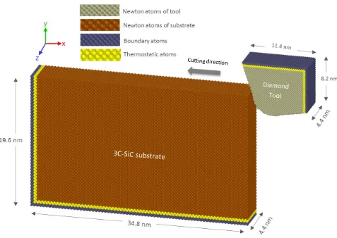
atomic/molecular massively parallel simulator” (LAMMPS) [12]. The three-dimensional nanometric cutting model of 3C-SiC is demonstrated in Fig. 1. Basically, this model is a plane-stress condition representation of realistic machining process. Both 3C-SiC workpiece and diamond
cutting tool are built as deformable bodies. The region of atoms in the tool and the workpiece are
divided into three different zones: boundary atom zone, thermostatic atom zone and Newtonian
atom zone, in accord with the previously published studies [13-17]. The boundary atoms serve as rigid bases for the workpiece and tool and would maintain the symmetry of the lattice. The
thermostatic atoms are allowed to follow Berendsen thermostatic dynamics to ascertain plausible
outward heat conduction away from the machined zone which is carried away by chips and
lubricants during actual machining. The Newtonian atoms whose behaviour is directed by the
motion equations arising from their Hamiltonian are allowed to follow the Newtonian dynamics
(LAMMPS NVE dynamics). In order to minimize the boundary effects, the length and height of the
workpiece and cutting tool are selected adequately large.
The temperature of the atoms during the machining simulation can be computed using the following
conversion between the kinetic energy and temperature:
T Nk v m b i i i 2 3 2
1
2 (1)
where N is the number of atoms, vi represents the velocity of ith atom, kb is the Boltzmann constant
(1.3806503×10⁻²³ J/K) and T represents the atomistic temperature. However, the instantaneous
fluctuations in kinetic energy (K.E.) of atoms would be very high so K.E. should be averaged (time
and/or spatial) over few timesteps to convert into equivalent temperature. Since the movement of
the cutting tool contributes to the kinetic energy, a modified kinetic energy should be applied so as
5 T Nk v
v
m b
i
tool i i
2 3 2
1
2 2 (2)
where vtoolis the velocity of cutting tool. While calculating the temperature for tool, It is possible to
[image:5.595.58.535.214.552.2]use temp/com command, which this automatically subtracts the tool velocity.
Fig. 1. Schematic of the MD simulation model
Interatomic potential function plays a pivotal role in the accuracy and reliability of the MD
simulation results. Erhart and Albe [11] proposed a three-body potential function called ABOP formalism so as to dictate the interactions between the atoms within the Si-Si, C-C and Si-C. Both
bulk and dimer properties such as binding energy, D0, the equilibrium bonding distance, r, and the
6
Hence, ABOP function was employed in this study to model hot nanometric cutting of single
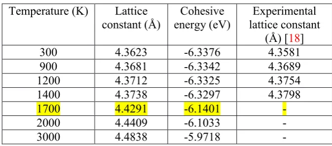
crystal 3C-SiC. In order to obtain accurate simulation results, the corresponding equilibrium lattice
constants for the studied cutting temperatures i.e. 300 K, 900 K, 1200 K, 1400 K, 1700 K, 2000 K
and 3000 K were calculated and accordingly were utilized to build the geometry of the workpiece.
The cohesive energy corresponding to the equilibrium lattice constant of 3C-SiC obtained from the
simulation at various temperatures are summarized in Table 1. In all cases, the tool was equilibrated at 300 K before simulations; hence the lattice constant of 3.568 Å calculated using the ABOP
[image:6.595.128.465.346.494.2]function at 300 K was used for the carbon atoms.
Table 1. Calculated equilibrium lattice constants and cohesive energies of single crystal 3C-SiC at different temperatures using ABOP function [11]
Temperature (K) Lattice constant (Å)
Cohesive energy (eV)
Experimental lattice constant
(Å) [18]
300 4.3623 -6.3376 4.3581
900 4.3681 -6.3342 4.3689
1200 4.3712 -6.3325 4.3754
1400 4.3738 -6.3297 4.3798
1700 4.4291 -6.1401 -
2000 4.4409 -6.1033 -
3000 4.4838 -5.9718 -
To avoid the interaction between workpiece and tool atoms at the beginning of simulation, the
cutting tool was placed at a distance of 10 Å (1 nm) away the workpiece surface. The model was
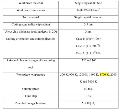
then allowed to run for 30 ps to achieve the desired temperature. Table 2 lists the geometry details and process parameters used in this study. The nanometric cutting trials were simulated by
advancing the tool atoms at every time step giving the tool a velocity of 50 m/s. This cutting speed
was employed primarily due to limitation of computational power since implementation of
parametric investigations at realistic cutting speeds (~1-2 m/s) would require very long computation
7
Table 2. Details of the MD simulation model and the cutting parameters used in the study
Workpiece material Single crystal 3C-SiC
Workpiece dimensions 34.8×19.6×4.4 nm3
Tool material Single crystal diamond
Cutting edge radius (tip radius) 3.5 nm
Uncut chip thickness (cutting depth in 2D) 3 nm
Cutting orientation and cutting direction Case 1: (010)<100>
Case 2: (110)<001̅>
Case 3: (111)<1̅10>
Rake and clearance angle of the cutting
tool
-25° and 10°
Workpiece temperature 300 K, 900 K, 1200 K, 1400 K, 1700 K, 2000
K and 3000 K
Cutting speed 50 m/s
Time step 1 fs
Potential energy function ABOP [11]
3. Results and discussion
3.1. Cutting forces and specific cutting energy
From the MD simulation standpoint, the cutting forces can be calculated by summing up the total
forces exerted by the carbon atoms of the cutting tool to the 3C-SiC workpiece. The force
components along the x, y and z directions describe tangential, thrust and axial forces, respectively.
Surface form error is chiefly affected by thrust force since this component of force has tendency to
separate the tool away from the workpiece. The tangential force brings about displacements in the
8
behaviour changes dynamically i.e. wear, fracture, elastic-plastic transition, displacement of the
material, heat generation, wear of the tool, dislocation slip etc. leading to change of the force as per
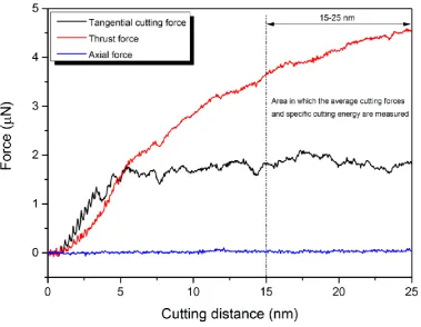
along the length of cut. The magnitude of the average tangential cutting forces, thrust forces,
resultant forces and specific cutting energy for all the studied temperatures and crystal planes has
been summarized in Table 1A in Appendix A. The average values of the forces were calculated only after the tool penetrated in the workpiece by 15 to 25 nm, as shown in Fig. 2.At the beginning stage of cutting, both the tangential and thrust forces are zero. As the diamond cutting tool starts moving
towards the single crystal 3C-SiC workpiece, the negative forces are observed, as illustrated in Fig. 2, signifying the effects of long-range attraction forces. Atoms attract each other when the instantaneous distance between two atoms is longer than the equilibrium distance between them. As
the cutting tool advances more, cutting forces on the tool atoms alter to repulsive and climb
proportionally, in a sense of average, with the cutting length. From Table 1A in Appendix A, it is conspicuous that the values of tangential, thrust and resultant forces decrease with the rise of
workpiece temperature for various crystal surfaces. With the increase of temperature, the amplitude
of atomic vibration within the workpiece increases. It is regarded as an increase in the number of
phonons. This phenomenon results in generating atomic displacements. The atomic displacements
within the workpiece causes a rise in the interatomic distances and a decrease in the restoring forces
owing to thermal expansion, resulting in lowering the energy needed to break the atomic bonds. As
a consequence, thermal softening occurs which reduces the cutting force required to deform the
9
Fig. 2. An MD output of the force plot showing the region where the average cutting forces and specific cutting energy were measured
The machinability and cutting resistance of materials can be indicated by the “specific cutting
energy”, which is the energy required to remove a unit amount of material. The specific cutting
energies can be calculated by dividing the resultant force by the chip area or volume, and it is
expressed in N/m2 or J/m3 [6]. In general, the lower the specific cutting energy, the higher the
efficiency of the cutting process is. Fig. 3 shows that large specific cutting energy values correspond to low workpiece temperatures since the 3C-SiC workpiece at a low temperature is more difficult to
be deformed. It can be also observed that the (111) crystal plane requires least specific cutting
energy while the highest magnitudes emerge on the (110) orientation. Hence, it can be deduced that
the (111)<1̅10> crystal setup is the easy orientation setup for cutting 3C-SiC. This particular
behaviour of 3C-SiC is similar to another important semiconductor, silicon [6]. Table 3 highlights the percentage reduction in the specific cutting energy during hot nanometric cutting with respect to
10
energy reduces up to 33% while cutting the (111) crystal plane at 2000 K. Also, it can be inferred
that at high temperatures, i.e. 2000 K and 3000 K, the minimum reduction in specific cutting energy
appears on the (111) plane whereas at lower temperatures the maximum reduction emergies on this
plane. Fig. 4 illustrates the variation of crystallography-induced anisotropy in the specific cutting energy as a function of workpiece temperature. It can be seen that the anisotropy increases from
~30% at 300 K to ~44% at 1400 K and afterwards it decreases to ~36%, ~24% and ~22% at 1700
K, 2000 K and 3000 K, respectively. The trend is on the contrary to the anistropy in specific cutting
[image:10.595.106.493.305.641.2]energy of siliocn, where it constantly increased with the increase of cutting temperature [6].
11
Table 3. Percentage reduction in specific cutting energy of 3C-SiC at high temperatures relative to room temperature
Crystal orientation
% reduction in cutting energy at
1400 K compared to 300
K
% reduction in cutting energy at
2000 K compared to 300
K
% reduction in cutting energy at
3000 K compared to 300
K
(010) Up to 19% Up to 43% Up to 60%
(110) Up to 9% Up to 38% Up to 54%
[image:11.595.104.495.101.630.2](111) Up to 27% Up to 33% Up to 48%
12 3.2. Chip formation and characteristics
During nanometric cutting, the cutting edge of the tool penetrates into the workpiece atoms and
separates the atoms near the tool tip. The separated atoms slide off along the rake face of the cutting
tool at a constant velocity in a stationary flow, leading to the formation of cutting chip. A stagnant
region ahead of the cutting tool divides the plastic flow into upward and downward directions, as
shown in Fig. 5. In other words, above the stagnation region, atoms flow up along the rake face and consequently form the chip. Underneath the stagnation region, atoms compress downward into the
workpiece leading to the formation of the freshly machined surface. The location of the stagnation
region can be determined through calculation of the average displacement of workpiece atoms in y
direction in various layers. Fig. 6 represents displacements of different layers in the workpiece when nanometric cutting of 3C-SiC is performed on the (110) crystal surface at 1400 K. Slope
alternation of the displacement line from positive to negative is an indication of the stagnation zone.
To be more precise, in the stagnation region the displacement line has an almost zero slope. Table 4
13
Fig. 5. Schematic view of chip formation demonstrating the stagnation region and five distinct zones within the workpiece: I- Cut zone, II- Below the flank face, III- Between the flank face and tool tip IV- Ahead and underneath the tool tip, V- Uncut zone. 𝜃𝑠1,2 and ℎ1,2 show the limiting bounds of the stagnation region.
Fig. 6. Displacement of various layers in y direction while cutting 3C-SiC on the (110) crystal plane at 1400 K
It can be deduced from Table 4 that while cutting the (111) crystal plane at different temperatures, the stagnation region is located at an upper position than other planes, which indicates ploughing
caused by compression is more pronounced on the (111) surface and therefore a thicker deformed
region is expected to be generated, which may result in higher elastic recovery. The converse
scenario occurs for the (110) orientation, where the stagnation region is located at a lower position
than those of other crystal orientations. It can be also inferred that at high temperatures the
stagnation region is located lower than that at room temperature, attributable to the thermal
softening and enhanced plasticity of 3C-SiC workpiece. Interestingly, it is found that the 3C-SiC
exhibits the same general trend observed for the position of stagnation region during nanometric
[image:13.595.107.486.151.430.2]14
magnitudes of stagnation angle and friction angle. The stagnation angle (𝜃𝑠) illustrated in Fig. 5 was calculated from:
𝜃𝑠1,2 = 𝑐𝑜𝑠−1(1 −ℎ1,2
𝑟 ) (3)
where ℎ1,2 and r are the limit bounds of stagnation region and tool tip radius, respectively. While
using a rounded edge tool, the friction angle (β) can be also calculated from:
𝛽 = 𝛼𝑒𝑓+ 𝑡𝑎𝑛−1(𝐹𝑐
𝐹𝑡) (4)
𝛼𝑒𝑓= 𝑠𝑖𝑛−1(1 −𝑑
𝑟)
where 𝛼𝑒𝑓 stands for the effective rake angle, Fc and Ft , respectively, represent the tangential and
thrust forces, and d is the uncut chip thickness. It is observed from Table 4 that up to 1400 K, the values of stagnation and friction angle are closely correlated for the (110) crystallographic
orientation. Nonetheless, there exists a discrepancy between two angles while cutting the (010) and
(111) planes or at high temperatures i.e. 2000 K and 3000 K, particularly the difference is more
[image:14.595.59.545.514.746.2]marked for the high cutting temperatures.
Table 4. Stagnation region, stagnation angle and friction angle while cutting 3C-SiC Workpiece
Temperature
(K)
Crystal
orientation
Position of stagnation region
from bottom of the tool (ℎ1,2)
(nm)
Stagnation angles
(𝜃𝑠1,2) (degree)
Friction angle
(β) (degree)
300
(010) 0.9-1.1 42-46.7 33
(110) 0.6-0.8 34-39.9 34.3
15 900
(010) 0.8-1 39.9-44.4 32.4
(110) 0.5-0.7 31-36.9 32.2
(111) 1-1.2 44.4-48.9 44.9
1200
(010) 0.7-0.9 36.9-42 32.7
(110) 0.5-0.7 31-36.9 31.1
(111) 0.7-0.9 36.9-42 45.7
1400
(010) 0.6-0.8 34-39.9 34.1
(110) 0.4-0.6 27.7-34 32.2
(111) 0.7-0.9 36.9-42 47.4
1700
(010) 0.6-0.8 34-39.9 36.5
(110) 0.3-0.5 23.9-31 36.2
(111) 0.7-0.9 36.9-42 46.8
2000
(010) 0.5-0.7 31-36.9 37.8
(110) 0.3-0.5 23.9-31 39
(111) 0.6-0.8 34-39.9 49
3000
(010) 0.2-0.4 19.5-27.7 40.1
(110) 0.1-0.3 13.7-23.9 41.3
16
It has been reported that during nanometric cutting of 3C-SiC on the (111) plane at room
temperature, cleavage occurs ahead of the cutting tool [20]. Indeed, it is generalized that cleavage is a dominant mechanism on the (111) crystal orientation, and the (111) plane is the most commonly
observed fracture plane of 3C-SiC. In order to realize whether cleavage takes place in nanometric
cutting on the various crystallographic orientations at elevated temperatures, the chip formation
process was carefully examined and the local environment of atoms up to the second neighbour
shell was monitored. Fig 7 illustrates the chip formation at three stages together with the evolution of cutting forces while cutting the (111) crystal surface at 1400 K. Crystallites of 3C-SiC in the
cutting chip can be observed, suggesting the occurrence of cleavage at high temperature of 1400 K.
In fact, the cleavage was observed to occur for all the simulated temperatures, 300 K-3000 K, while
cutting the (111) surface, which have not been shown here for the purpose of brevity. However, at
high temperature of 3000 K, smaller amount of crystallites were observed in the chip in comparison
to those of lower temperatures, plausibly due to improved plasticity at this temperature. The
substantial dominance of the (111) cleavage plane can be attributed to the lower cleavage energy
and fracture surface energy of this plane as opposed to the other crystal orientations. This specific
characteristic of 3C-SiC is comparable with that of diamond [21]. As evident from Fig. 7 (b), cutting forces experience an abrupt drop at the points where cleavage occurs, resultant from flaking
off the crystallite of 3C-SiC without undergoing amorphization. Thus, as the cutting tool does not
17 (a)
(b)
[image:17.595.63.532.58.679.2]18
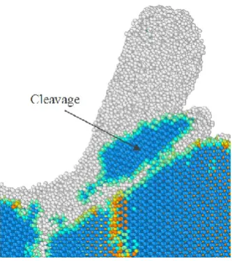
While cleavage is anticipated to be dominant on the (111) orientation, a shift to the (110) cleavage
at the cutting temperatures higher than 2000 K was seen during nanometric cutting processes , as
shown in Fig 8. It is of note that the event of cleavage was observed to occur alongside with the formation and annihilation of stacking fault-couple, locks and cross-junctions between pairs of
counter stacking faults [22]. Such (110) cleavage event is in accord with the earlier observations on the diamond under blunt indentations at high temperature [23], where shear stresses and plastic flow are thought to dictate the failure and the stress fields are inhomogeneous. It should be mentioned
here that the diamond shares the same cubic lattice structure in its sp3 bonded state with 3C-SiC.
Hence, similarities in the material behaviour under contact loading problems could be expected.
Note that very small amount of remnants of cleavage was observed for some other cases, i.e. on the
(010) and (110) at 300 K.
Fig. 8. Snapshot from the MD simulation showing the event of cleavage while cutting the (110) crystal plane at 2000 K
[image:18.595.215.382.443.631.2]19
highest number of atoms in the chip appears on the (111) plane; however it drops at 3000 K. As
mentioned earlier, large volume of cleavage is occurred while cutting the (111) crystal plane thus it
is sensible to observe higher number of atoms in the chip while cutting the (111) plane.
Furthermore, as seen in Fig. 10, the depth of subsurface deformation layer becomes deeper when the temperature of workpiece rises. As noted earlier, increase of the workpiece temperature will
weaken interatomic bonding which triggers more crystal deformation within subsurface atoms.
Thus, the layer depth of deformation becomes larger. This specific behaviour seemingly appears to
be common in both single crystal 3C-SiC and silicon [4]. Another light can be brought by Fig. 10 is that the depth of subsurface deformation layer is the highest on the (111) plane whereas it is the
lowest on the (110) orientation. The occurrence of cleavage and pronounced ploughing due to
compression as a result of the upper position of stagnation region on the (111) plane could have the
key role in this observation.
[image:19.595.103.497.422.714.2]20
Fig. 10. Subsurface deformation layer depth as a function of cutting temperature and crystal orientation
Fig. 11 shows the variation of resultant force exerted by the tool rake face on the chip, and friction coefficient at the tool rake face/chip interface while cutting 3C-SiC on different crystallographic
planes at various temperatures. Clearly, the values of resultant force exerted by the tool rake face on
the chip are found to be smallest while cutting 3C-SiC on the (111) crystal plane whereas they are
largest on the (110) orientation, which is consistent with the previous observations in this study. The
friction coefficient at the tool rake face/chip interface varies from 0.42 to 0.9 on different crystal
planes and temperatures. It may be noted that the friction coefficient is minimum on the (111)
orientation. A remarkable observation is that the friction coefficient at the tool rake face/chip
interface on the (110) and (010) orientations increases in the temperature range of 300 K to 1200 K
and 300 K to 900 K, respectively, as opposed to the (111) crystal plane, where the friction
[image:20.595.110.491.57.352.2]21
Fig. 11. Variations of the resultant force exerted by the tool rake face on the chip, and friction coefficient at the tool rake face/chip interface while cutting 3C-SiC on different crystallographic planes at various temperatures
The theory of heat release in the primary, secondary and tertiary deformation zones is well
documented. During nanometric cutting, heat is generated owing to the energy release as a result of
the breaking and reformation of bonds in the primary deformation zone and owing to the friction at
the interface of the cutting tool and the workpiece. The generated heat in the primary deformation
zone is transferred into the chip thus the chip carries a great amount of heat during its separation
from the workpiece. To investigate the heat generated during chip formation process and
consequently the extent of temperature increase (due to the generated heat) from the initial substrate
temperature, an elemental atomic volume (1×1.5×3 nm3 including 442 atoms) was considered in the
primary deformation zone and the variations of the temperature were monitored on this volume. It
can be observed from Fig. 12 that while cutting the (111) plane in the temperature range of 300 K to 1400 K, the extent of temperature increase caused by the generated heat in the deformation zone is
[image:21.595.86.517.66.369.2]22
form of heat during occurrence of cleavage on this crystallographic orientation. However, at 2000
K, the amount of release of heat is smaller than those at lower temperatures due to the weaker
bonding between atoms. As stated above, the generated heat in the deformation region is dissipated
into the chip thus it is not surprising to see the similar trend for the chip temperature, as depicted in
Fig. 13. It must be mentioned here that there may exist some inconsistencies in the observed trends in this study since a multifaceted interplay of various variables such as adhesive forces, interfacial
energies, contact areas, number of dangling bonds, nanoscale friction etc. changes with the
[image:22.595.98.495.325.621.2]temperature and crystallographic orientation during nanometric cutting at elevated temperatures.
23
Fig. 13. Chip temperature as a function of cutting temperature and crystal plane
3.3. Plastic flow behaviour
In order to investigate the plastic deformation mediated flow behaviour of 3C-SiC during
nanometric cutting, the atomic flow field in various zones of the workpiece was determined. Fig. 14
illustrates the displacement vector of atoms after 20 nm of cutting at 300 K on the (010), (110) and
(111) orientations. A very clear distribution of atomic flow field is apparent in various zones of the
workpiece. It can be drawn from Fig. 14 that the atoms beneath the cutting tool in region ΙΙΙ experience a rotational flow. This particular flow behaviour of 3C-SiC is analogous to what was
observed in our previous study concerning nanometric cutting of silicon [3] and other materials [24]. Nevertheless, there are some discrepancies i.e., in region ΙV, the motion of atoms along the cutting direction is much more marked for the 3C-SiC than silicon workpiece. In particular, with the
(111) orientation at 300 K, the movement of atoms along the [1̅1̅1̅] direction alters to the [2̅01̅].
This behaviour can be attributed to the occurrence of cleavage ahead of the cutting tool. Another
24
observed for the silicon. The upwards motion of 3C-SiC atoms is more remarkable on the (111)
surface plausibly due to the higher elastic recovery, as a consequence of higher ratio of hardness to
Young’s modulus (H/E), and upper position of stagnation region (see section 3.2), on this crystal
orientation as opposed to the other planes. Similar to silicon, the centre of rotational flow
underneath the tool while cutting 3C-SiC on the (111) orientation was found to be positioned lower
than those of other crystal surfaces, which assists a more effective flow of the atoms within the
workpiece. It can, therefore, facilitate the chip formation and material removal during nanometric
cutting process. This observation could confirm why the lowest specific cutting energy was realized
25
Fig. 14. Atomic flow field in the XY plane during nanometric cutting of 3C-SiC on the various crystal planes at 300 K. The location of the cutting tool in connection with the different regions can be traced from Fig. 5.
As can be seen from Fig. 15, when nanometric cutting of 3C-SiC is carried out at 3000 K, the rotational flow of the atoms in region ΙΙΙ is practically eliminated. This fact is more discernible for
the (111) crystallographic orientation and atoms show a little turbulence flow. Moreover, as a result
of weak van der Waals interactions between atoms at high temperature of 3000 K, the workpiece
[image:25.595.59.541.50.551.2]26
upward motion of atoms in region I even at high temperature of 3000 K. Accordingly, one would
expect to perceive elastic recovery at this temperature. The reason for such observation could be
traced at the melting point of 3C-SiC predicted by the ABOP function.A common problem intrinsic
to bond order potentials (BOP) for semiconductors is the overestimation of melting point. An
attempt was made to calculate the melting point of 3C-SiC predicted by ABOP using one-phase
method and adopting reflective boundaries to diminish the hysteresis phenomenon [25-26]. The phase instability and entirely molten temperature of a 15 × 15 × 15 supercell were observed at
3529 K and 3993 K, respectively, which are far above the experimental value (~2800 K). Therefore,
satisfactory thermal softening and in turn decline of elastic recovery which ought to be occurred at
27
Fig. 15. Atomic flow field during nanometric cutting of 3C-SiC on the various crystallographic surfaces at 3000 K
3.4. Stress, temperature and wear of the cutting edge of the tool
Figs. 16 and 17 demonstrate the variation of average von Mises stress and temperature measured on the cutting edge of the diamond cutting tool during nanometric cutting of single crystal 3C-SiC on
[image:27.595.59.542.49.569.2]28
average magnitude of von Mises stress measure, Tresca stress measure and temperature on the
[image:28.595.115.485.139.436.2]cutting edge in all the simulated test cases.
29
Fig. 17. Variation of temperature measured on the cutting edge of the diamond tool while cutting different orientations of 3C-SiC at different cutting temperatures
It can be observed from Fig. 16 that the cutting tool experiences least stress and temperature on the (111) crystal plane compared to others, which makes it an easy cutting plane, consistent with the
observed trend in critical von Mises stress to cause yielding of 3C-SiC during nanometric cutting
[22]. Besides, the values of stresses on the cutting edge decrease with the increase of workpiece temperature for the different crystallographic planes. The magnitudes of Mises stress and Tresca
stress acting on the cutting edge of the cutting tool at low and high temperatures are found to be in
the range of 38 to 68 GPa and 21 to 38 GPa, respectively. Clearly, the stress values are lower than
95 GPa [27], which is the minimum stress obtained by first-principle calculation to cause structural instability in the diamond structure. However, as can be seen in Fig. 17, the average temperature on the cutting edge spans from 680 K to 1060 K for the different workpiece temperatures and
crystallographic orientations. A representative illustration of the temperature distribution on atoms
30
at some atoms on the cutting edge might reach 3000 K but due to high heat conductivity of diamond
and usage of thermostatic atoms (to ascertain plausible outward heat conduction away from the
machined zone which is carried away by cutting chips and lubricants during actual machining), the
average temperature on the cutting edge is in the range of 680 K to 1060 K.
[image:30.595.169.428.439.654.2]Fig. 18. Temperature distribution on atoms while cutting the (110) crystal plane at 3000 K
Fig. 19. The hardness of diamond as a function of temperature [28]
31
that the hardness of diamond decreases to ~52 GPa and ~33 GPa, respectively, at temperatures of
680 K and 1060 K. On the other hand, at these temperatures i.e. 680 K and 1060 K, the average von
Mises stress acting on the cutting edge is found to be 61.4 GPa while cutting the (010) surface and
63.5 GPa while cutting the (110) plane, respectively. Accordingly, it is not surprising to witness
plastic deformation of cutting tool and tool wear via atom-by-atom attrition during nanometric
cutting of 3C-SiC at different temperatures, as demonstrated in Fig. 20. It is of note that, up to the workpiece temperature of 1400 K, abrasive action between atoms of diamond cutting tool and
3C-SiC workpiece culminates in increasing the temperature on the cutting edge. However, at higher
temperatures, due to enhanced thermal softening and decrease of the hardness of workpiece,
abrasive action would be mitigated; hence a slight decrease in the temperature on the cutting edge is
visible in Fig. 17. Consequently, it can be seen from Fig. 20b that at a workpiece temperature of 2000 K, the atom-by-atom attrition wear is quantitatively less severe than that of 1400 K, which
correlates highly with the amount of stresses on the cutting edge at these temperatures. Moreover,
the shape of the cutting tool is found to be somewhat deformed while cutting at 1400 K in
comparison with that of 2000 K. These observations confirm that while cutting at high
temperatures, the atom-by-atom attrition wear and plastic deformation of the diamond cutting tool
could be alleviated. However, chemical wear i.e. dissolution-diffusion and adhesion wear may be
32 (a)
(b)
Fig. 20. Atom-by-atom attrition wear and plastic deformation of diamond cutting tool while nanometric cutting of 3C-SiC at a) 1400 K b) 2000K
4. Conclusions
Due to superior properties of 3C-SiC, this material has been in the centre of focus as a compound
semiconductor to be utilized in the fabrication of devices operating under harsh conditions, leading
to a potential demand for cost effective manufacturing of complex 3C-SiC components with mirror
finish. Nanometric cutting is now an established ultra-precision manufacturing method to obtain
mirror finish and damage-free surfaces with significant cost reduction. However, in nanometric
cutting of brittle materials i.e. 3C-SiC, the diamond tool faces tremendous cutting resistance. In
such cases, methods are required to be identified to reduce the cutting resistance offered by the
substrate so as to improve the machinability. A common understanding about 3C-SiC is that high
temperature reduces the yield strength and hardness, and improves the fracture toughness which in
turn improves its plastic deformation. However, its extent has never been reported as this knowhow
could be vital in implementing the hot machining of 3C-SiC with the assistance of Laser
processing. This process can open up new horizons for new commercial, technological and
[image:32.595.102.508.82.316.2]33
temperature electronics and sensors used in spacecrafts and aircrafts, power devices, microwave
electronics used in radar systems, and other applications in the biomedical sector. Taking into
account the aforementioned points, MD simulation was employed to investigate the process of
nanometric cutting of 3C-SiC on different crystallographic planes i.e. the (010), (110) and (111)
under a wide range of workpiece temperatures (300 K-3000 K) in order to shed some light on the
mechanisms involved in this process. The primary findings are as follows:
1. The anisotropy in the specific cutting energy initially increased with the increase of
cutting temperature up to 1400 K and then decreased at higher temperatures i.e. 1700 K
and 2000 K.
2. The stagnation region was seen to be positioned at a lower position on the (110) crystal
plane or at elevated temperatures. Further analysis revealed that the stagnation and
friction angles were closely correlated while cutting the (110) crystal plane in the
temperature range of 300 K-1400 K.
3. A shift to the (110) cleavage at the cutting temperatures higher than 2000 K was
witnessed. Moreover, crystallites of 3C-SiC in the cutting chip was observed in the all
simulated temperatures while cutting the (111) plane. Nevertheless, at 3000 K, the
amount of cleavage was smaller than those of lower temperatures.
4. The increase of cutting temperature led to the formation of deeper subsurface
deformation layer. Maximum damage depth for the preferred cleavage plane of the (111)
was found to be consistently larger than those of other planes.
5. The values of resultant force exerted by the tool rake face on the cutting chip were found
to be smallest while cutting 3C-SiC on the (111) crystal plane whereas they were largest
on the (110) surface. Furthermore, the friction coefficient at the tool rake face/chip
interface was minimum on the (111) orientation. The friction coefficient at the tool rake
face/chip interface on the (111) was observed to constantly decrease with the increase of
34
6. Much higher extent of temperature increase caused by the generated heat in the
deformation region was witnessed while cutting the (111) plane in the cutting
temperature range of 300 K to 1400, plausibly due to occurrence of cleavage on this
crystallographic orientation.
7. Atoms beneath the cutting tool were found to experience a rotational flow, which is
practically analogous to the plastic flow behaviour of silicon. The elimination of vortex
flow at the cutting temperature of 3000 K was more manifest for the (111)
crystallographic orientation than other surfaces.
8. According to the stress state on the cutting edge of the diamond cutting tool, the
atom-by-atom attrition wear and plastic deformation of the diamond cutting tool were seen to
be alleviated while cutting at high temperatures i.e. 2000 K. However, chemical wear
viz. dissolution-diffusion and adhesion wear could be accelerated at high temperatures.
Acknowledgments
SZC would like to thank the help of Dr. Saurav Goel from Queen’s University, Belfast, UK for his
useful advice. The authors gratefully acknowledge the financial support from the EPSRC
(EP/K018345/1) and Royal Society-NSFC international exchange programme (IE141422) for this
study. The authors also acknowledge the use of the EPSRC (EP/K000586/1) funded ARCHIE-WeSt
High Performance Computer at the University of Strathclyde.
Appendix A
Table 1A. Average forces and specific cutting energy while cutting single crystal 3C-SiC on
different crystallographic orientations at various temperatures
[image:34.595.113.483.705.764.2]35
(K) cutting
force (nN) force (nN) force (nN) cutting energy (GPa) 300
(010) 2112 4564.8 5029.7 381
(110) 2280.5 4660.6 5188.6 393.1
(111) 2122.3 2943.1 3628.5 274.9
900
(010) 1863.7 4156.8 4555.5 345.1
(110) 1988 4462.9 4885.7 370.1
(111) 1781 2393.4 2983.4 226
1200
(010) 1869.7 4100.4 4506.6 341.4
(110) 1888.5 4463.5 4846.6 367.2
(111) 1741.6 2270.7 2861.7 216.8
1400
(010) 1792.9 3691.4 4103.8 310.9
(110) 1934.8 4349.3 4760.2 360.6
(111) 1680.3 2062.3 2660.1 201.5
1700
(010) 1604.7 2983.1 3387.3 256.6
(110) 1841.1 3459.6 3919 296.9
(111) 1554.9 1947.8 2492.3 188.8
2000
(010) 1433.6 2526.2 2904.7 220
(110) 1672.7 2804.8 3265.7 247.4
(111) 1606.3 1864.1 2460.7 186.4
3000
(010) 1067.1 1717 2021.6 153.1
(110) 1330.6 2039.5 2435.2 184.5
(111) 1267.6 1402.9 1890.8 143.2
36
Table 1B. Average stresses and temperature on the cutting edge of the diamond tool while cutting
single crystal 3C-SiC on different crystallographic orientations at various temperatures
Workpiece temperature (K) Crystal orientation von Mises
stress on the
cutting edge (GPa) Tresca stress on the cutting edge (GPa) Temperature on the cutting edge (K) 300
(010) 66 38 773.6
(110) 67.7 38.3 927.8
(111) 61.4 34.3 679.1
900
(010) 61.2 34.3 878.5
(110) 66.5 38 1037.3
(111) 56.8 32.6 729.9
1200
(010) 60.4 34.1 937.2
(110) 65.6 37 1049.8
(111) 55.7 32.9 733.9
1400
(010) 59.8 33.7 958.9
(110) 63.5 36.3 1060.3
(111) 54.1 31.3 783.8
37
1700 (110) 58.9 35.3 1010.4
(111) 46.6 28.9 775.3
2000
(010) 48.9 27.1 909.5
(110) 54.3 30.1 983
(111) 41.7 22.6 758.6
3000
(010) 44.5 24.7 871.4
(110) 46.5 25.2 919.8
(111) 38.5 21.1 738.2
References
[1] P. Mélinon, B. Masenelli, F. Tournus, A. Perez, Playing with carbon and silicon at the
nanoscale. Nature Materials 6 (2007) 479-490
[2] S. Goel, W.B. Rashid, X. Luo, A. Agrawal, V. K. Jain, A theoretical assessment of surface
defect machining and hot machining of nanocrystalline silicon carbide. Journal of Manufacturing
Science and Engineering, 136 (2) (2014) 021015
[3] S. Z. Chavoshi, S. Goel, X. Luo, Molecular dynamics simulation investigation on plastic flow
behaviour of silicon during nanometric cutting. Modelling Simul. Mater. Sci. Eng. 24 (2016)
015002
[4] S. Z. Chavoshi, X. Luo, An atomistic simulation investigation on chip related phenomena in
nanometric cutting of single crystal silicon at elevated temperatures. Computational Materials
38
[5] S. Z. Chavoshi, S. Xu, X. Luo, Dislocation-mediated plasticity in silicon during nanometric
cutting: A molecular dynamics simulation study, Materials Science in Semiconductor Processing,
51, (2016) 60-70
[6] S. Z. Chavoshi, S. Goel, X. Luo, Influence of temperature on the anisotropic cutting behaviour
of single crystal silicon: A molecular dynamics simulation investigation. Journal of Manufacturing
Processes, Accepted
[7] T-H Fang, C-I Weng, J-G Chang, Molecular dynamics analysis of temperature effects on
nanoindentation measurement. Materials Science and Engineering A, 357 (2003) 7-12
[8] C-L Liu, T-H Fang, J-F Lin, Atomistic simulations of hard and soft films under nanoindentation.
Materials Science and Engineering A 452-453 (2007) 135-141
[9] J-Y Hsieh, S-P Ju, S-H Li, C-C Hwang, Temperature dependence in nanoindentation of a metal
substrate by a diamond-like tip. Physical Review B (2004) 70, 195424
[10] H. Zhao, P. Zhang, C. Shi, C. Liu, L. Han, H. Cheng, L. Ren, Molecular dynamics simulation
of the crystal orientation and temperature influences in the hardness on monocrystalline silicon.
Journal of Nanomaterials, (2014) Article ID 365642
[11] P. Erhart, K. Albe, Analytical potential for atomistic simulations of silicon, carbon, and silicon
carbide. Physical Review B, 71(3) (2005) 035211
[12] S. Plimpton, Fast parallel algorithms for short-range molecular-dynamics. Journal of
computational physics, 117 (1) (1995) 1-19
[13] J. Belak, Nanotribology: modelling atoms when surfaces collide Energ. Tech. Rev. (1994), pp.
39
[14] N. Chandrasekaran , A. Noori Khajavi , L. M. Raff, R. Komanduri, A new method for
molecular dynamics simulation of nanometric cutting. Philosophical Magazine Part B, 77:1, 7-26
(1998)
[15] R. Komanduri, N. Chandrasekaran, and L. M. Raff, Molecular dynamics simulation of
atomic-scale friction. Phys. Rev. B 61, 14007 (2000)
[16] R. Komanduri , N. Ch and rasekaran & L. M. Raff (2001) Molecular dynamics simulation of
the nanometric cutting of silicon, Philosophical Magazine Part B, 81:12, 1989-2019.
[17] R. Komanduri, N. Chandrasekaran & L. M. Raff (1999) Some aspects of machining with
negative-rake tools simulating grinding: A molecular dynamics simulation approach, Philosophical
Magazine Part B, 79:7, 955-968
[18] Z. Li, R. C. Bradt, Thermal expansion of the cubic (3C) polytype of SiC. Journal of Materials
Science 21 (1986) 4366-4368
[19] A. Stukowski, Visualization and analysis of atomistic simulation data with OVITO-the Open
Visualization Tool. Modelling Simul. Mater. Sci. Eng. 18 (2010), 015012
[20] S. Goel, A. Stukowski, X. Luo, A. Agrawal, R. L. Reuben, Anisotropy of single-crystal 3C-SiC
during nanometric cutting. Modelling Simul. Mater. Sci. Eng. 21 (2013) 065004
[21] J. E. Field, The mechanical and strength properties of diamond. Rep. Prog. Phys. 75 (2012)
126505
[22] S. Z. Chavoshi, X. Luo, Molecular dynamics simulation study of deformation mechanisms in
3C-SiC during nanometric cutting at elevated temperatures. Materials Science and Engineering: A,
654 (2016) 400-417
[23] C. A. Brookes, E. J. Brookes, V. R. Howes, S. G. Roberts, and C. P. Waddington, A comparison
of the plastic deformation and creep of type I, type II and synthetic diamonds at 1100°C under
40
[24] G.L. Cross, B.S. O'Connell, H.O. Özer, J.B. Pethica. Room temperature mechanical thinning
and imprinting of solid films, Nano Lett 7 (2007) 357-362
[25] H. T.T. Nguyen, V. V. Hoang, L. N. T. Minh, Melting of crystalline silicon thin films.
Computational Materials Science 89 (2014) 97-101
[26] Q. Zhang, Q. Li, M. Li, Melting and superheating in solids with volume shrinkage at melting:
A molecular dynamics study of silicon. The journal of chemical physics 138 (2013) 044504
[27] H. Chacham, L. Kleinman, Instabilities in diamond under high shear stress. Physical Review
Letters 85(23) (2000) 4904-4907
[28] M. B. Cai, X. P. Li, M. Rahman, Study of the temperature and stress in nanoscale ductile
mode cutting of silicon using molecular dynamics simulation. Journal of Materials Processing