Abstract:A novel high-k gate dielectric material, i.e., Lanthanum-doped Zirconium oxide (La-doped ZrO2), has been
thoroughly studied for applications in future metal oxide semiconductor field-effect transistor (MOSFET). The film's structural, chemical and electrical properties are investigated experimentally. The incorporation of La into ZrO2 impacted the
electrical properties in terms of leakage current while not sacrificing its dielectric constant. The dielectric constant of 25 is achieved which is calculated from the C-V analysis taken from Agilent 1500A Semiconductor Device Analyzer. XRD, FTIR, EDX analysis were conducted to confirm the stoichiometry and bond formation of La2Zr2O7. The sol-gel spin coating method is adopted
to form a uniform thin film over p-Silicon substrate and Aluminium is evaporated in the eBeam technique as gate electrode to form an MIS capacitor. The La-doped ZrO2 film is
hence a potential high-k gate dielectric for future application in MIS thin film transistors.
Keywords: La2Zr2O7, MOS capacitor, High-k, Gate capacitor,
dielectric constant, thin film.
I. INTRODUCTION
H
igh-k materials presently under investigation are Al2O3, CeO2, ZrO2, TiO2, HfO2, Ta2O5, La2O3, Er2O3,Pr2O3,Gd2O3, Y2O3, etc. and some of their silicates such as
AlxZr1-xO2, ZrxSi1-xOy, HfxSi1-xOy, etc. however, many of
these materials show less thermodynamic stability on Si, also few other properties which need to be taken care of are; good adhesion, deposition at low temperature, large breakdown voltage, low defect density, ability to be patterned easily and low charge states on silicon. To find a best substitute for SiO2, in addition to the high-k value, the high-k materials should have several sophisticated characteristics. They should have good interface properties with the Si substrate, chemically stable with Si substrate and the gate electrode, should be thermally stable-at temperatures no less than 500°C. The structure can have high channel mobility, low interface trap density, large bandgap, low oxide trap density, low leakage current density, large band off-set energies and
Revised Manuscript Received on September 06, 2019
Mohammad Hayath Rajvee*, Center for Nanotechnology, AU College of Engineering (A), Andhra University, Visakhapatnam -5320003, Andhra Pradesh, India. [email protected].
P.Rajesh Kumar, Professor, Department of Electronics and Communication Engineering, AU College of Engineering (A), Andhra University, Visakhapatnam -5320003, Andhra Pradesh, India.
Y.Srinivasarao, Professor, Department of Instrument Technology, AU College of Engineering(A), Andhra University, Visakhapatnam -5320003, Andhra Pradesh, India. [email protected]
equivalent oxide thickness (EOT) – 10 to 15Å, High dielectric constant (10 < high-k < 50). All these guidelines are met by only few of these materials whereas many dielectrics are favorable in some of these areas. Including these, the bulk and interface properties of the new dielectric material must be comparable to the remarkable properties of SiO2. Since an important function of the gate dielectric is to isolate the gate terminal from the current-carrying channel region, it needs to be a good insulator. Lanthanum Zirconate nanocrystallites have high dielectric constant (k~22-30), wide energy band gap (~6eV), high crystallization temperatures, and good stability with Si. Also, it has been demonstrated as the thermal barrier coatings and showed excellent thermal stability because of its cubic pyrochlore structure [9–14]. Hence, we expect it can be used as a good gate dielectric for the future of MOSFET generations.
II. EXPERIMENTAL
La2Zr2O7 solution was prepared using the sol-gel method.
Initially, 5gms of Zirconium Oxychloride Octahedrate (ZrOCl2.8H2O) (Sigma Aldrich) powder was dissolved in
50ml of ethanol(C2H6O) and stirred at an optimum stirring
speed using magnetic stirrer and the solution was leveled to form a clear and transparent solution. The mixture was then stirred continuously for 30min at 500C and 350rpm. 5.01gms of 99.9% pure lanthanum oxide (La2O3) (Sigma Aldrich)
powder dissolved in 25ml of ethanol (C2H6O) in a 100ml
beaker, this solution was then stirred for 5hrs at 90oC and 500rpm. Subsequently, lanthanum solution was added dropwise to the zirconium precursor solution and stirred for another 1hr at 100oC and 350rpm. To achieve a stoichiometric lanthanum zirconate in 1:1M ratio of La/Zr was maintained. After a homogeneous mixture was obtained, the resulting La2Zr2O7 was cooled down before spin-coating
on an RCA(Radio Corporation of America) Cleaned p-Si (100 orientation) substrate (with a resistivity of 5-10Ω-cm) wafers were cut down into small pieces of 1cm X 1cm square shape before depositing LZO solution. The spinning rate was 4000rpm and spinning time was 30sec. After spun, sample was placed in a furnace for post-deposition annealing at 130oC with a heating rate of 18oC-min-1 for 15min. The sample was then cooled down to room temperature. Spin deposition process was repeated ten times to achieve a uniform ultrathin LZO (Lanthanum zirconate) passivation layer. The novel procedure adopted in this work is to achieve a higher dielectric constant than that of the earlier reported works.
Aluminium was deposited by e-beam evaporation method in a vacuum chamber at a background pressure up to 5x10⁻⁵ Pa. 200µm X 200µm front contact was made through hand-made shadow masking. Aluminium
metal was evaporated on the complete back surface of Si
Fabrication and Characterization of amorphous
Lanthanum Zirconate Gate Capacitors
substrate to act as a back contact. The use of a metal contact as the dielectric surface, and highly doped Si wafer as a substrate completes the parallel plate capacitor device. The metal contact deposition was established using e-beam evaporation for 200µm X 200µm area. The deposition rate was maintained at 1Å /s till the thickness reached to 150nm.
[image:2.595.307.544.50.421.2]III. RESULTSANDDISCUSSION
Figure 1: XRD diffraction pattern of lanthanum doped ZrO2
The XRD diffraction pattern of Lanthanum doped ZrO2 as in
Figure 1. No clear peak in the graph represents the amorphous nature of the material. Crystallite size calculated using Bragg's law is 32nm. On heating, the material will acquire crystallite nature at 6000C and the miller indices can be calculated.
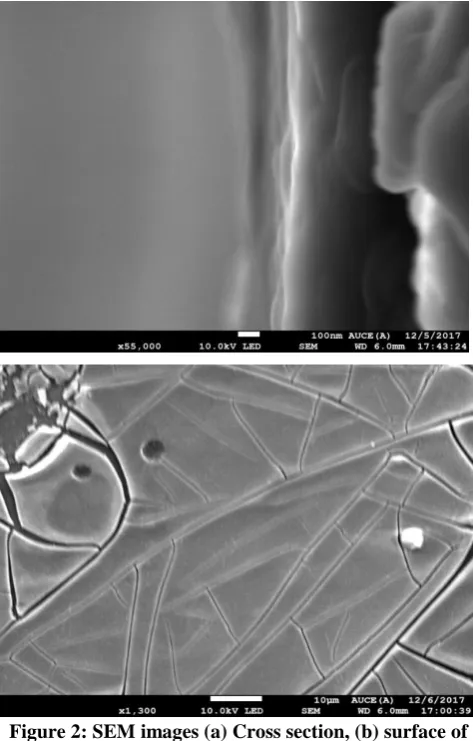
Figure 2(a) shows the cross sectional SEM image of Lanthanum doped ZrO2 film. Formation of a nano thin film is
clearly visible. From the microstructure, it can be concluded that dopant has modified the film growth process and by consequence the microstructure and surface morphology. The Lanthanum doped ZrO2 film shown in figure 2(b)
represents a uniform coating and the surface appearing less porous. The cracks and delaminations that were found are consistent with the existing literature.
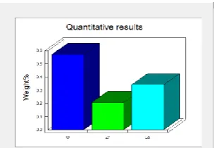
The Lanthanum doped thin film calcinated at 1300C was analyzed by energy dispersive spectroscopy as shown in Figure 3 and Figure 4 respectively. EDS analysis of La2Zr2O7
film shows that Lanthanum, Zirconium and Oxygen are the detected elements and thus presence of lanthanum and zirconium in the ratio of 1:1 was confirmed.
The following figure 4 indicated the bar chat for thin film of Lanthanum doped Zirconium high-k Dielectric gate capacitor confirming the presence of La2Zr2O7. The atomic weight
percentage proves that the sample synthesized has a good stoichiometry with a good compromise of materials
Figure 2: SEM images (a) Cross section, (b) surface of Lanthanum doped ZrO2 films
Figure 3: EDX Spectrum analysis of lanthanum doped zirconium oxide
Element Weight% Atomic%
OK 0.57 88.26
Zr L 0.21 5.65
La L 0.34 6.09
Totals 1.12 -
TABLE1:ELEMENTAL COMPOSITION OF LA2ZR2O7
[image:2.595.54.284.258.448.2]Figure 4: Bar chart of lanthanum and zirconium Figure 5 shows the FTIR spectra of spin coated La2Zr2O7 thin
films. The band at 2560.43cm–1 indicates vibration of Zr-O bond. Ali Bahari [5] investigated ZrO2 thin films deposited
[image:3.595.308.544.46.526.2]by sol-gel spin coating technique and obtained a similar type of microstructure. The band at 3700cm–1 corresponds to the vibration of the Si-O bond.
Figure.5: FTIR Spectra Of Spin Coated La2Zr2O7 Figure 6 indicates the AFM images of sol-gel spin coated Lanthanum Zirconate high-k dielectric thin film. The 3D image the layer shows a smooth surface with uniform distribution of material. Scan is performed at a random location in an area of 1μm x 1μm. These results are further correlated with electrical properties achieved in other characterizations. The film resulted in a surface area ratio of 4.31% representing large linearity of the deposited film. A random location is chosen from the scanned region to plot the line profile of the film. It shows an average variation of 6.5nm in the surface profile shown in Figure 8. Uniform thin film has resulted from the sol-gel spin coat technique at room temperature. The grain boundary results of AFM shown in Figure 8 supports the film linearity as it showed very fewer grains.
[image:3.595.94.247.49.154.2]Figure.6: 3D Surface Image obtained from PARK XE-7 AFM
Figure 7. Grain boundaries on film surface
Figure.8: Line Profile of the deposited film C-V measurements of Al/La2Zr2O7/p-Si were carried out by
using Agilent 1500A Semiconductor Device Analyzer and plotted in Figure 9. Three distinct regions of the C-V graph are accumulation, depletion and inversion which are clearly visible at the interface. The maximum capacitance was achieved in the accumulation for negative voltage. Because, the majority charge carriers (holes) of p-substrate will form a conduction layer at the interface. The maximum capacitance in this region was found to be 859pF,163pF and 2.74pF respectively for 1KHz, 100KHz and 1MHz applied frequencies respectively. This wide dispersion observed in the accumulation region is because of the substrate series resistance. Effect substrate series resistance will be more prominent as the frequency increases. The dielectric constant calculated with the values of C-V curve is 25 using equation 4. The curves were corrected for the calculation of dielectric constant (Wu et al 2006).
[image:3.595.55.290.256.397.2] [image:3.595.67.273.589.717.2]K= Ctox/(ƐA) (4)
where C is Accumulation capacitance, tox oxide thickness, Ɛ
is permittivity of free space and A is the area of the gate
[image:4.595.50.281.97.293.2]electrode. Equivalent Oxide thickness was measured using EOT= (ksio2.tox)/kx (5)
Figure 9: C-V Characteristics of spin coated La2Zr2O7 film
where value of ksio2 is 3.9, tox is oxide layer thickness(44 nm)
and kx dielectric constant of LaZrO4 layer fabricated (25);
value of EOT calculated is 5.4 nm. A slight positive shift of 0.4V in the flatband voltage(Vfb) is observed. This is because of the negative charges present in the LZO thin film.
Effective oxide charges (Qeff) located in La2Zr2O7thin film.
Qeffis given by
Qeff
=
[image:4.595.55.285.406.598.2]
(6)
Figure 10: Leakage current Vs Gate voltage which is calculated as 1.098x10¹⁵Cm-12. A positive shift in flatband voltage Vfb can be identified from CV analysis.
Maximum leakage current measured is 10nA; which is shown in figure 10. This value is lower than the reported leakage current..
IV. CONCLUSION
The main focus of this work was to study structural, topographical and electrical characteristics of high-k dielectric layer of Lanthanum zirconate (La2Zr2O7). Initially,
La2Zr2O7 solution is prepared through sol gel method and it is
deposited using spin coating method at 4000 rpm spun for 30Sec. The as prepared film's amorphous nature was
confirmed by XRD analysis, the EDX report obtained is supporting stoichiometry of 1:1 nature of the prepared gel. The deposited film thickness is measured to be 31.5nm using ellipsometer. Calculated EOT is 5.4nm. Presence of uniform thin dielectric layer was confirmed by cross sectional SEM image. Aluminium is thermally evaporated using eBeam evaporation as a gate electrode. Thus an Al/La2Zr2O7/p-Si/Al
capacitor is formed; and analysed for AC and DC characteristics with Agilent 1500A Semiconductor Device Analyzer electrometer for C-V analysis and I-V analysis. The measured dielectric constant (k) is 25 and the gate leakage current measured to be 10nA. All the calculated values are tabulated in table number 2.
V. FUTURESCOPE
The deposited films can be undertaken for annealing at various temperatures like 4000C, 5000C, and 6000C to study the crystal orientation of the material (phase formation) which in turn changes the dielectric constant, leakage current and Equivalent Oxide thickness.
Physical Oxide layer
thickness - tox 31.5nm Dielectric Constant - k 25
Equivalent Oxide
thickness (EOT) 5.4nm
Qeff
1.098x101
5Cm-12
Gate Leakage Current 10nA
Vfb 0.4V
TABLE 2:MEASURED /CALCULATED PARAMETERS OF THE GATE CAPACITOR
10. So Yeon Je, Byeong-Geun Son, Hyun-Gwan Kim, Man-Young Park, Lee-Mi Do, Rino Choi, and Jae Kyeong Jeong, “Solution- Processable LaZrOx/SiO2 Gate Dielectric at Low Temperature of 180 °C for High-Performance Metal Oxide Field- Effect Transistors”, ACS Appl. Mater. Interfaces 2014, 6, 18693−18703
11.Mohammad Hayath Rajvee, P. Rajesh Kumar, Y. Srinivasarao,
“Fabrication and Characterization of
Cerium Doped Zirconium Oxide High-K Dielectric thin film Gate Capacitors by solgel spin coating technique to investigate the spin rate dependence of dielectric constant and EOT for VLSI/ULSI technologies” J. of Adv Res. in Dynamical & Control Systems, Vol. 10, 13-Special Issue, 2018.
14. Mohammad Hayath Rajvee, P.Rajesh Kumar, Y.Srinivasarao, “Effect of pre synthesis sintering on bandgapg of CeZrO4 nano crystalline powders prepared through high energy ball milling for high k dielectric thin films”, DOI: 10.1109/SPACES.2018.8316334, ieee xplore
15. K.Praveen Kumar, Kumaraswamy Gajula “Fractal Array antenna Design for C-Band Applications”, International Journal of Innovative Technology and Exploring Engineering (IJITEE), Volume-8 Issue-8 June, 2019.
16. K.Praveen Kumar, “Active Switchable Band-Notched UWB Patch Antenna”, International Journal of Innovative Technology and Exploring Engineering (IJITEE), Volume-8 Issue-8 June, 2019. 17. K.Praveen Kumar, “Circularly Polarization of Edge-Fed Square Patch
Antenna using Truncated Technique for WLAN Applications”, International Journal of Innovative Technology and Exploring Engineering (IJITEE), Volume-8 Issue-8 June, 2019.
18. K.Praveen Kumar, “Triple Band Edge Feed Patch Antenna; Design and Analysis”, International Journal of Innovative Technology and Exploring Engineering (IJITEE), Volume-8 Issue-8 June, 2019. 19. K.Praveen Kumar, Dr. Habibulla Khan "Optimization of EBG structure
for mutual coupling reduction in antenna arrays; a comparitive study" International Journal of engineering and technology, Vol-7, No-3.6, Special issue-06, 2018.
20. K.Praveen Kumar, Dr. Habibulla Khan "Active PSEBG structure design for low profile steerable antenna applications" Journal of advanced research in dynamical and control systems, Vol-10, Special issue-03, 2018.
21. K.Praveen Kumar, Dr. Habibulla Khan, "Design and characterization of Optimized stacked electromagnetic band gap ground plane for low profile patch antennas" International journal of pure and applied mathematics, Vol 118, No. 20, 2018, 4765-4776.
22. K.Praveen Kumar, Dr Habibulla Khan " Surface wave suppression band, In phase reflection band and High Impedance region of 3DEBG Characterization" International journal of applied engineering research (IJAER), Vol 10, No 11, 2015.
23. K.Praveen Kumar, Dr. Habibulla Khan " Active progressive stacked electromagnetic band gap structure (APSEBG) structure design for low profile steerable antenna applications" International Conference on Contemporary engineering and technology 2018 (ICCET-2018) March 10 - 11, 2018. Prince Shri Venkateshwara Padmavathy Engineering College, Chennai.
24. K.Praveen Kumar, Dr. Habibulla Khan "Optimization of EBG structures for Mutual coupling reduction in antenna arrays; A comparative study" International Conference on Contemporary engineering and technology 2018 (ICCET-2018) March 10 - 11, 2018. Prince Shri Venkateshwara Padmavathy Engineering College, Chennai.
25. K Satish Reddy a, K Praveen Kumar, Habibulla Khan, Harswaroop Vaish “Measuring the surface properties of a Novel 3-D Artificial Magnetic Material” 2nd International Conference on Nanomaterials and Technologies (CNT 2014), Elsevier Procedia material Science. 26. K.Praveen Kumar, "Mutual Coupling Reduction between antenna
elements using 3DEBG" IEEE International conference on communication technology ICCT-April-2015. Noor Ul Islam University Tamilnadu.
27. K.Praveen Kumar, "The surface properties of TMMD-HIS material; A measurement" IEEE International conference on communication technology ICCT-April-2015. Noor Ul Islam University Tamilnadu. 28. K.Praveen Kumar, "Design of 3D EBG for L band Applications" IEEE
International conference on communication technology ICCT-April-2015. Noor Ul Islam University Tamilnadu.
29. K.Praveen Kumar, "Effect of 2DEBG structure on Monopole Antenna Radiation and Analysis of It's characteristics" IEEE International
conference on communication technology ICCT-April-2015. Noor Ul Islam University Tamilnadu.
30. K.Praveen Kumar, Dr Habibulla Khan " The surface properties of TMMD-HIS material; a measurement" IEEE International conferance on electrical, electronics, signals, communication & optimization EESCO - January 2015.
31. B. Venkateswar Rao, Praveen Kumar Kancherla, Sunita Panda “Multiband slotted Elliptical printed Antenna Design and Analysis” Journal Of Mechanics Of Continua And Mathematical Sciences (JMCMS), Vol.-14, No.-4, July-August (2019) pp 378-386.
32. Kumaraswami Gajula, Amulya Boyina, K. Praveen Kumar “Active Quad band Antenna Design for Wireless Medical and Satellite Communication Applications” Journal Of Mechanics Of Continua And Mathematical Sciences (JMCMS), Vol.-14, No.-4, July-August (2019) pp 239-252.