Voltage Sag Compensation of Point of Common
Coupling (PCC) Using Fault Current Limiter
M. Jafari, Student Member, IEEE, S. B. Naderi, Student Member, IEEE, M. Tarafdar Hagh, Member, IEEE, S. H. Hosseini, Member, IEEE, M. Abapour, Student Member, IEEE
Faculty of Electrical & Computer Engineering, University of Tabriz, Tabriz, IRAN Email: [email protected]
Abstract-In this paper, voltage sag compensation of point of common coupling (PCC) using a new structure of fault current limiter (FCL) is proposed. The proposed structure prevents voltage sag and phase angle jump of substation PCC after fault occurrence. This structure has a simple control method. Using semiconductor switch (IGBT or GTO) at dc current rout leads to fast operation of the proposed FCL and consequently, dc reactor value is reduced. On the other hand, the proposed structure reduces total harmonic distortion (THD) on load voltage and it has low ac losses in the normal operation. As a result, other feeders which are connected to the substation PCC will have good power quality. Analytical analysis, simulation results using PSCAD/EMTDC software and experimental results are presented to validate effectiveness of this structure.
Index Terms─Voltage sag, fault current limiter, power quality,
point of common coupling (PCC), semiconductor switch, THD.
I. INTRODUCTION
Electric power quality can be defined as the capacity of an electric power system to supply electric energy of a load in an acceptable quality. Many problems can result from poor power quality, especially in today's complex power systems, such as false operation of modern control systems. Voltage sag is an important power quality problem because of sensitive loads growth. Worldwide experience shows that short circuit faults are the main origin of voltage sags and therefore the loss of voltage quality. This problem appears especially in buses which are connected to radial feeders [1-6].
The most common compensator for voltage sag is dynamic voltage restorer (DVR). The basic operation of the DVR is based on injection a compensation voltage with required magnitude, phase angle and frequency in series with sensitive electric distribution feeder [7, 8].
The voltage sag during the fault is proportional to the short circuit current value. An effective approach to prevent expected voltage sag and improve the voltage quality of point of common coupling (PCC) is fault current limitation by means of a device connected at the beginning of most exposed radial feeders [9].
Superconducting fault current limiter (SFCL) structures have proper characteristics to control the fault current levels due to their variable impedance in the normal and fault conditions [10-13]. However, because of high technology and cost of superconductors, these devices are not commercially available. Therefore, by replacing the superconducting coil with non-superconducting one in the FCL, it is possible to make it simpler and much cheaper. It is important to note that, the main drawback of non-superconductor is a power loss which is
negligible in comparison with the total power, provided by distribution feeder [14, 15].
The other structures which are introduced in [4, 16, 17], have two numbers of thyristor switches in AC branch of diode bridge. When the fault occurs, after fault detection, thyristor switch turns off at first zero crossing and the fault current is limited to an acceptable value. These structures have switching power loss and complicated control circuit because of thyristor switching in the normal operation. In addition, we know that thyristor operation delay (turn off at first zero crossing) makes interruption on structure performance. So, to limit the fault current between fault occurrence instant and thyristors turn off instant, a large reactor in dc route is used. Because of voltage drop, harmonic distortion and power losses, this large value of dc reactor is unfavorable.
In this paper a new topology of FCL is proposed for the voltage sag and the phase angle jump mitigation of the substation PCC. In section II, analytical analysis of voltage sag and phase angle jump is discussed. Then, in section III, the proposed FCL topology is introduced and its operation in a simplified power system is explained. In section V, the PSCAD/EMTDC software is applied to investigate the operational behavior of the proposed FCL in this power system and simulation results are analyzed. Experimental results are presented and adapted with the simulations in section VI.
II. VOLTAGE SAG STUDY IN SIMPLIFIED POWER SYSTEM
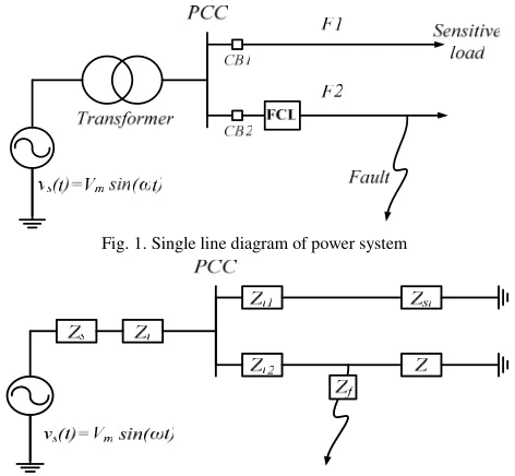
Fig. 1 shows single line diagram of the power system. This figure shows a substation with only two feeders F1 and F2. However, the presented analysis can be extended to any number of feeders, easily. The F1 supplies a sensitive load. With a fault in the F2, the voltage sag occurs in the substation PCC.
Positive sequence equivalent circuit of such a system is shown in Fig. 2. To calculate the voltage sag, the simple voltage divider method is introduced in [18].
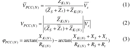
In the normal state, the voltage magnitude and its phase angle in the substation PCC can be expressed as follows:
( ) ( )
( )
( )
K N
PCC N s
t
S K N
Z
V V
Z Z Z
=
+ +
(1)
( ) ( )
( )
( )
K N
PCC N s
t
S K N
Z
V V
Z Z Z
=
+ +
(2)
( ) ( )
( )
( ) ( )
arctan( K N ) arctan( K N S t)
PCC N
K N K N S t
X X X X
R R R R
ϕ = − + +
+ +
[image:1.612.342.565.627.710.2]Fig. 1. Single line diagram of power system
Fig. 2. Positive sequence equivalent circuit of the case study system in the fault condition
where:
( ) PCC N
V : Voltage phasor of PCC in the normal state;
( ) PCC N
V : Voltage magnitude of PCC in the normal state;
( ) PCC N
ϕ : Phase angle of PCC voltage in the normal state where, the phase angle of Vs is considered to be zero;
: t
Z Phasor of transformer impedance; :
S s s
Z =R + jX Phasor of source impedance; :
S
V Phasor of source voltage;
( ) ( ) ( ):
K N K N K N
Z =R + jX Equivalent impedance of parallel
feeders in the normal condition, i.e.:
1 2
( ) ( L SL) ( L )
K N
Z = Z +Z Z +Z (4)
Z : Phasor of load impedance at the F2.
In the normal state, ZK N( ) is greater than ZS+Zt . So, the PCC voltage is almost equal to the source voltage.
In the fault condition in the F2, the voltage and phase angle of substation PCC can be expressed as follows:
( ) ( )
( )
( )
K F
PCC F s
t
S K F
Z
V V
Z Z Z
=
+ +
(5)
( ) ( )
( )
( )
K F
PCC F s
t
S K F
Z
V V
Z Z Z
=
+ +
(6)
( ) ( )
( )
( ) ( )
arctan( K F ) arctan( K F S t)
PCC F
K F K F S t
X X X X
R R R R
ϕ = − + +
+ +
(7)
where:
( ) PCC F
V : Voltage phasor of PCC during fault;
( ) PCC F
V : Voltage magnitude of PCC during fault;
( ) PCC F
ϕ : Phase angle of voltage of PCC during fault;
( ) ( ) ( ):
K F K F K F
Z =R + jX Equivalent impedance of parallel
feeders during fault, i.e.:
( ) ( 1 ) ( 2 )
K F L SL L F
Z = Z +Z Z +Z (8)
F
Z : Fault impedance.
In three phase fault condition (that is a balance fault.), ZF equals to zero approximately and according to Eq. (8), ZK F( )
and Eq. (3) with Eq. (7) show that the voltage sag and the phase angle jump occur in the fault interval, respectively. So, the sensitive load experiences worse condition. To prevent voltage sag and phase angle jump during fault, a proper solution is introducing a large limiting impedance between the substation PCC and the fault location. This solution is the base of FCL’s operation.
III. PROPOSED FCL CONFIGURATION AND ITS OPERATION
Fig. 3 shows the circuit topology of the proposed FCL which is composed of two following parts:
1. Bridge part that includes a diode rectifier bridge, a small dc limiting reactor (Ldc) (Note that, its resistance (Rdc) is involved, too.), a semiconductor switch (IGBT or GTO), a free wheeling diode (D5).
2. Shunt branch as a compensator that consists of a resistor and an inductor (Rsh+ j Lω sh).
Previously introduced structures for this application [4, 16, 17], have used two numbers of thyristors at bridge branches instead of one semiconductor switch inside the bridge (dc current route). Therefore, firstly, they have the more complicated control system. Secondly, in those structures, because of thyristors operation delay (turn off at first zero crossing), Ldc has large value to limit the fault current between fault occurrence instant and thyristors turn off instant, properly. This large value of Ldc leads to considerable voltage drop on the FCL and the power losses including ac power losses on the shunt branch impedance and dc reactor power losses (if it is non-superconductor) in the normal condition. By using the semiconductor switch in the proposed structure and its fast operation, it is possible to choose a small value for Ldc to prevent sever di dt at the beginning of fault occurrence. So, the voltage drop and power losses will be negligible. Nowadays, high rating semiconductor switches are available in practice. However, using self turn off switch instead of thyristors in the proposed structure leads to more cost [19-21]. From power loss point of view, in the normal condition, the proposed FCL has the losses on the rectifier bridge diodes, the semiconductor switch and Rdc. Each diode of the rectifier
[image:2.612.359.518.564.711.2]bridge is ON in half a cycle, while semiconductor switch is always ON. Therefore, the power losses of this FCL in the normal operation can be calculated as Eq. (9).
2
.
4
loss R D SW dc dc DF ave SWF dc
P =P +P +P =R I + V I +V I (9)
where:
Idc : dc side current which is equal to peak of line current
(Ipeak);
VDF : Forward voltage drop on each diode;
VSWF : Forward voltage drop on the semiconductor switch;
Iave. : Average of diodes current in each cycle that is equal to
peak
I π .
Considering Eq. (9) and the small value of dc reactor in this structure, total power losses of the proposed structure becomes a very small percentage of the feeder’s transmitted power. For example, by considering Table I parameters in simulation section, the power losses will be 0.47% of the feeder’s transmitted power.
On the other hand, in the fault condition, the PCC voltage drops on the shunt impedance. Therefore, the line current will pass through the shunt resistor (Rsh). As a result, power loss on
the Rsh depends on its value that will be discussed in design
considerations section. Note that the fault condition is several cycles and it is a small time interval.
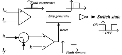
IV. CONTROL STRATEGY
Fig. 4 shows the control circuit of the proposed FCL. In the normal operation of the power system, the semiconductor switch is ON and the line current (iL) passes through “D1, Ldc, semiconductor switch, D4” and “D3, Ldc , semiconductor switch, D2” in positive and negative alternatives, respectively. So, L dc is charged to peak of the line current and behaves as a short circuit. Using semiconductor devices (diodes and semiconductor switch) and small dc reactor, cause a negligible voltage drop on the FCL.
When a fault occurs, Idc become greater than maximum
permissible current Im and control circuit detects it and turns
the semiconductor switch off. So, the bridge retreats from the feeder and the shunt impedance enters to the faulted line and limits the fault current. At this moment, the free wheeling diode discharges Ldc. In fact, the free wheeling diode is used to provide free route for dc reactor current when the semiconductor switch is OFF.
When fault is removed, while semiconductor switch is OFF, shunt impedance will be connected in series with the load impedance. Therefore, line current will be decreased, instantaneously. To detect this instantaneous reduction of line current, iL is compared with (If) that can be calculated from Eq. (10).
Fig. 4. Control circuit of the proposed FCL
PCC f
sh sh V I
R j Lω =
+ (10)
When the difference of iL and If become greater than k as the fault removal sign, control circuit turns the semiconductor switch ON. So, power system returns to the normal state. The value of k can be calculated from Eq (11) as follow:
,min
PCC PCC
sh sh L
V V
k
Z Z Z
= −
+
(11)
where:
Zsh : The shunt impedance;
ZL,min : Minimum impedance of load on the protected feeder.
V. DESIGN CONSIDERATIONS
As mentioned previously, Ldc is placed in series with the semiconductor switch to protect it against severe di dt at the beginning of fault occurrence. So, its value can be chosen considering current characteristic of the semiconductor switch.
For designing shunt branch parameters, it is possible to consider following conditions. In the ideal case, shunt branch impedance is equal to load impedance. In this condition, when a fault happens in the protected feeder, the voltage sag at the PCC will be zero. However, it is difficult to equate these impedances exactly because of load variation on distribution feeders. So, it is difficult to estimate the best value for Lsh and
sh
R . From practical point of view, parameters of shunt branch can be determined by using the history of load measurements at the protected feeder. It is obvious that feeder’s power and consequently its current change. For calculation of Lsh and
sh
R values, average impedance of the protected feeder is calculated. So, Lsh and Rshare chosen equal to its inductance and resistance.
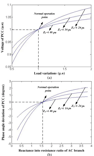
From practical point of view, Fig 5(a) and Fig. 5(b) are considered. Fig. 5(a) shows the magnitude of PCC voltage. The horizontal axis of this figure shows the magnitude of load impedance in per-unit where the base value is its impedance of ideal case. The dashed line shows the existence of ideal case. The ratio of reactance to resistance of shunt branch is kept constant in this figure. The parameter of this figure is the magnitude of source impedance. This figure shows that for a wide range of load magnitude variations (0.5 to 2 p.u. with fixed shunt branch impedance), the voltage magnitude of PCC for post-fault condition changes in an acceptable range especially for low values of ZS .
[image:3.612.72.280.630.724.2](a)
(b)
Fig. 5. (a) Voltage magnitude and (b) Phase angle deviation of the PCC when shunt branch impedance is not equal to the protected feeder load
impedance (non-ideal case).
VI. SIMULATION RESULTS AND EFFECT OF THE PROPOSED FCL ON VOLTAGE SAG AND PHASE ANGLE JUMP
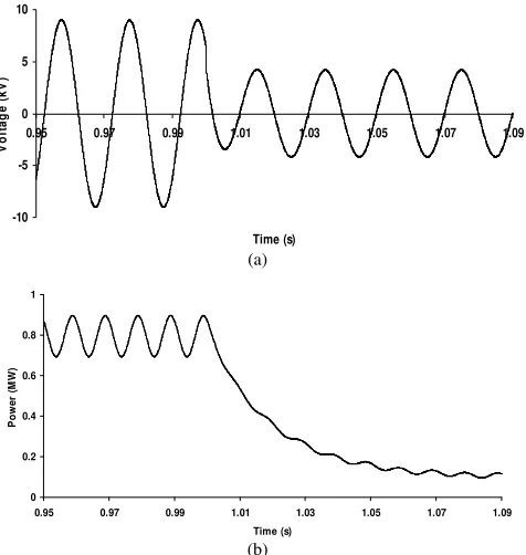
[image:4.612.73.262.41.355.2]With a balanced fault at the F2 in Fig. 1, without using the FCL, the PCC voltage drops, severely. When the FCL is installed in the F2, not only reduces the fault current, but also restores the non-faulted feeder voltage to the normal level. So, the FCL improves the voltage quality and the reliability of the supply network. In this section, analytical analysis of the proposed FCL and simulation results are presented. System parameters are as Table I. These simulations are obtained using the PSCAD/EMTDC software. In addition, considering section IV, to show the practical condition, the values of shunt branch parameters (Rsh, Lsh) are the non-ideal case.
Table I. System parameters
Power source 20kV, 50Hz, X/R ratio: 5 Total Impedance: 1.608 Ω Source Side Data
Transformer 20 kV/6.6 kV, 10 MVA, 0.1 pu
Feeder F1 j0.314 Ω Distribution
feeders data Feeder F2 j0.157 Ω
dc side
dc
L = 0.01 H, Rdc= 0.03 Ω
3 , 3 , 0.6
DF SWF m
V = V V = V I = kA Switch type: IGBT
FCL data
Shunt branch Lsh= 0.08 H, Rsh= 5 Ω
Sensitive load 10+ j15.7 Ω Load data
Load of F2 15+ j31.4 Ω
0 1
t = s), the PCC voltage and power transfer to the sensitive load drop without the FCL. Considering this figure, it shows that zero crossing of the PCC voltage changes before and after fault. With placing the proposed FCL in outset of the F2, when the fault happens, the proposed FCL inserts large impedance into the faulted line and prevents the voltage sag and phase angle jump at the substation PCC. Fig. 7 shows the PCC voltage and sensitive load single phase power in this condition. In the first moments of fault, slight distortion appears in the PCC voltage waveform caused by the semiconductor switch operation and inserting the shunt impedance into the faulted line. After that, the PCC voltage sag and phase angle jump will be in an acceptable range that is discussed in section IV in detail. The power of the sensitive load in this interval has not any considerable change.
In comparison with operation of the structures introduced in [4], [16] and [17], using the semiconductor switch at dc current route in the proposed FCL instead of thyristors at bridge branches, leads to mitigation of sag and distortion in the PCC voltage after fault occurrence (Fig. 8). As shown in simulation results, the proposed FCL can resolve voltage sag and phase angle jump problem properly.
Fig. 9 shows the voltage drop on the proposed FCL during fault. This voltage drop causes that the PCC voltage does not change (considering Fig. 7(a)).
Fig. 10 shows the line current of F2, dc reactor and shunt impedance current (i tL( ), idc( )t and ish( )t respectively). As shown in Fig. 10(b), between fault occurrence instant (t0) and line current rising to its normal condition’s peak instant (t1), the dc reactor current does not change. From instant t1 to t2 (semiconductor switch operation instant), the dc reactor charges according to differential Eq. (12).
1
( )
( ) 2
( )
dc
dc dc dc DF SWF PCC
dc peak
di t
L R i t V V V
d t
i t t I
ω
ω ω
ω
ω ω
+ + + =
= =
(12)
where:
( )
dc
i ωt : dc reactor current between t1 to t2; sin( )
PCC P
V =V
ω
t .Solution of Eq. (13) leads to:
1 ( )
( ) sin ( )
d c d c R
t t L
d c d c
i t A e B t K
ω ω
ω ω ϕ
− −
= + − + (13)
where:
1
2 2 2
2 2 2
2
sin( )
2
arctan( )
DF SWF
P
dc dc
dc
dc dc
P
dc dc
DF SWF
dc
dc dc
dc
V V V
A I t
R R L
V B
R L V V K
R L R
ω ϕ
ω
ω
ω ϕ
+
= − − +
+
=
+
+
= −
=
[image:4.612.46.574.565.726.2]-10 -5 0 5 10
0.95 0.97 0.99 1.01 1.03 1.05 1.07 1.09
Time (s)
V
o
lt
a
g
e
(
k
V
)
(a)
0 0.2 0.4 0.6 0.8 1
0.95 0.97 0.99 1.01 1.03 1.05 1.07 1.09
Time (s)
P
o
w
e
r
(M
W
)
(b)
Fig. 6. (a) PCC voltage and (b) Single phase instantaneous power of the sensitive load without FCL
-10 -8 -6 -4 -2 0 2 4 6 8 10
0.96 1.01 1.06 1.11 1.16 1.21 1.26
Time (s)
V
o
lt
a
g
e
(
k
V
)
(a)
0 0.1 0.2 0.3 0.4 0.5 0.6 0.7 0.8 0.9 1
0.96 1.01 1.06 1.11 1.16 1.21 1.26
Time (s)
P
o
w
e
r
(M
W
)
(b)
Fig. 7. (a) PCC voltage and (b) Single phase instantaneous power of the sensitive load with the proposed FCL
-10 -5 0 5 10
0.95 0.97 0.99 1.01 1.03 1.05 1.07 1.09
Time (s)
V
o
lt
a
g
e
(
k
V
)
PCC voltage with Thyristor switch in pervious structures PCC voltage with the proposed structure
(a)
0 0.2 0.4 0.6 0.8 1
0.95 0.97 0.99 1.01 1.03 1.05 1.07 1.09
Time (s)
P
o
w
e
r
(M
W
)
Transfer power with Thyristor switch in pervious structures Transfer power with the proposed structure
(b)
Fig. 8. (a) PCC voltage and (b) Single phase instantaneous power of the sensitive load waveforms with semiconductor switch in the proposed FCL and
thyristor switches in previously structures
-10 -8 -6 -4 -2 0 2 4 6 8 10
0.96 1.01 1.06 1.11 1.16 1.21 1.26
Time (s)
V
o
lt
a
g
e
(
k
V
[image:5.612.56.294.47.298.2])
Fig. 9. Voltage drop on the proposed FCL during fault
-0.7 -0.5 -0.3 -0.1 0.1 0.3 0.5 0.7
0.96 1.01 1.06 1.11 1.16 1.21 1.26
Time (s)
C
u
rr
e
n
t
(k
A
)
Im=0.6kA
(a)
Time
C
u
rr
e
n
t
Idc Line current Shunt impedance current
t0 t1 t2
Im
(b)
Fig. 10. (a) Line, dc reactor and shunt impedance currents and (b) enlarged view
In addition, at this interval, voltage across the proposed FCL increases shunt impedance current. Differential equation of this current is expressed by Eq. (15):
( )
( )
sh
sh sh sh PC C
di t
L R i t V
d t ω
ω ω
[image:5.612.314.561.52.173.2] [image:5.612.315.563.206.647.2] [image:5.612.54.298.325.722.2])
(
t
i
shω
1 ( )
( ) sin( )
sh sh R
t t L
sh sh
i t Ae B t
ω ω
ω ω ϕ
− −
= + − (16)
where:
1
2 2 2
2 2 2
sin( )
arctan ( )
P
sh
sh sh
P
sh sh
sh sh
sh
V
A t
R L
V B
R L
L R
ω ϕ
ω
ω ω ϕ
= − −
+
=
+
=
(17)
Note that the time interval between t1 to t2 is some
milliseconds.
Semiconductor switch control strategy is based on maximum permissible fault current, Im. Between t1 to t2, line current
(iL(ωt)) equals to idc(ωt) plus ish(ωt) (Fig. 10(b)). When semiconductor switch current exceeds Im, control system of its turns it off. In Eq. (13), if id c(ωt) is equal to Im , semiconductor switch operation instant (t2) can be calculated.
After t2, the diode bridge retreats and the shunt impedance
limits the fault current. Until fault clearance instant and turning on the semiconductor switch, the line current follows Eq. (16). In addition, at this interval, idc(ωt) is discharged by D5 as
following equation:
2
( )
( ) 0
( )
dc
dc dc dc
dc m
di t
L R i t
d t
i t t I
ω
ω ω
ω
ω ω
+ =
= =
(18)
As a result:
2
( )
( )
d c d c R
t t L
d c m
i t I e
ω ω ω
− −
= (19)
It is important to note that Eq. (16) is composed of two parts, exponential and sinusoidal. The Exponential part causes a transient in the line current (as shown in Fig. 10(a)) that duration of this transient depends on time constant of the shunt impedance (Lsh Rsh ).
VII.EXPERIMENTAL SETUP
To show effectiveness of the proposed FCL, an experimental setup is provided and its results are shown in this section. Table II shows parameters of the experimental study.
Fig. 11 shows the PCC voltage in a balanced fault condition by using the proposed FCL. This figure is in agreement with Fig. 7(a). It is obvious that the proposed FCL prevents the voltage sag with negligible distortion only because of semiconductor switch operation. In addition, the phase angle jump on the PCC voltage is mitigated, too
The voltage drop on the FCL is shown in Fig. 12. It is obvious that this figure follows Fig. 9. Fig. 13(a) and 13(b) show the line current of the F2 and the shunt impedance current, respectively. In general, the experimental setup validates the simulation results and shows that the proposed FCL has acceptable capabilities for the voltage quality improvement and the current limiting aims.
Power source 100V peak, 50Hz, 0.5 Ω Source Side Data
Transformer 100V/100V, 5kVA, 0.1 pu
Feeder F1 j0.2 Ω Distribution
feeders data Feeder F2 j0.2 Ω
dc side
dc
L = 0.01 H, Rdc= 0.03 Ω
1 , 2.5
DF m
V = V I = A
IGBT: 600V, 40A at 100
T= C, 2.5
SW V < V
FCL data
Shunt branch Lsh= 0.1 H, Rsh= 30 Ω
Sensitive load 30+ j47 Ω Load data
Load of F2 30+ j47 Ω
Fig. 11. The PCC voltage with the proposed structure (Volt/div.: 50V, Time/div.: 10ms)
Fig. 12. The voltage drop on the proposed FCL during Fault (Volt/div.: 50V, Time/div.: 25ms)
(a)
(b)
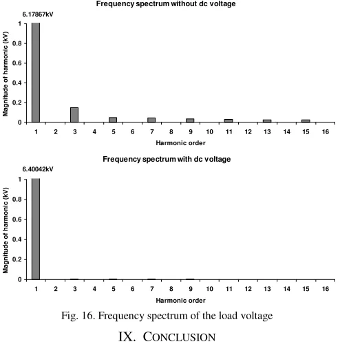
[image:6.612.317.560.54.711.2]VIII. HARMONIC STUDY
As mentioned above, because of using the diodes, the semiconductor switch and the small dc reactor, there is a voltage drop on the FCL. This voltage drop causes harmonic distortion on load voltage and power losses in shunt branch in normal condition.
Using dc voltage source in the proposed structure, Fig. 14, compensates voltage drop on the power electronic devices and the small dc reactor resistance. So, it reduces total harmonic distortion (THD) of voltage waveform [14, 22, and 23]. Its magnitude can be achieved by Eq. (20) as follow:
2
dc dc dc DF SWF
V =R I + V +V (20)
Where, VSWF and VDF stand for the voltage drops across the semiconductor switch and each diode, respectively. Idc is the current of dc route that is equal to the peak of line current in the normal condition. It is important to note that the dc voltage source can be simply provided by a rectifier [14, 15].
Fig. 15 shows load voltage in the normal operation of the power system with and without the dc voltage source and Fig. 16 shows frequency spectrum of the load voltage. By using the dc voltage source, the distortions of voltage waveform decreases to lower values in the normal condition, as shown in Fig. 14 and Fig. 16. THD of the load voltage in case of the proposed FCL without and with the dc voltage source are 2.789% and 0.117%, respectively.
D1 D2
D3 D4
Ldc
Switch
Lsh
Rsh
D5 Rdc
Vdc
Fig. 14. The proposed FCL topology with dc voltage source
Time (s)
V
o
lt
a
g
e
(
k
V
)
[image:7.612.318.565.51.301.2]Load voltage with dc voltage source Load voltage without dc voltage source Fig. 15. The load voltage in the normal operation of the power system with and
without the dc voltage source
Frequency spectrum without dc voltage
0 0.2 0.4 0.6 0.8 1
1 2 3 4 5 6 7 8 9 10 11 12 13 14 15 16 Harmonic order
M
a
g
n
it
u
d
e
o
f
h
a
rm
o
n
ic
(
k
V
)
6.17867kV
Frequency spectrum with dc voltage
0 0.2 0.4 0.6 0.8 1
1 2 3 4 5 6 7 8 9 10 11 12 13 14 15 16 Harmonic order
M
a
g
n
it
u
d
e
o
f
h
a
rm
o
n
ic
(
k
V
)
6.40042kV
Fig. 16. Frequency spectrum of the load voltage
IX. CONCLUSION
In this paper, the proposed FCL structure is introduced. Voltage sag compensation, phase angle jump mitigation and fault current limiting operation due to the control method were analyzed. The computer simulation using the PSCAD/EMTDC software and the experimental study are presented to validate results of the analytical analysis. The proposed FCL is capable of mitigating voltage sag and phase angle jump to acceptable levels. Because of using the semiconductor switch in dc current path instead of two numbers of thyristor at the bridge branches, the proposed FCL has high speed and consequently, dc reactor value is reduced to lower value. Note that the control system of this structure is simpler than previous ones. In addition, the dc voltage source placed in the proposed FCL structure reduces its THD and ac losses in the normal operation. In general, this type of FCL with the simple control circuit and low cost is useful for the voltage quality improvement because of voltage sag and phase angle jump mitigating and low harmonic distortion in distribution systems.
REFERENCES
[1] Jovica V. Milanovic, Yan Zhang, “Modeling of FACTS Devices for Voltage Sag Mitigation Studies in Large Power Systems,” IEEE Trans. Power Del., vol. 25, no. 4, pp. 3044-3052, Oct 2010.
[2] Timothy J. Browne, Gerald T. Heydt. “Power Quality as an Educational Opportunity,” IEEE Trans. Power Del., vol. 23, no. 2, pp. 814-815, May 2008.
[3] Nesimi Ertugrul, Ameen M. Gargoom, Wen. L. Soong. “Automatic Classification and Characterization of Power Quality Events,” IEEE Trans. Power Del., vol. 23, no. 4, pp. 2417-2425, Oct 2008.
[4] M. Abapour, Seyed Hossein Hosseini, M. Tarafdar Hagh. “Power Quality Improvement by Use of a New Topology of Fault Current Limiter,” ECTI-CON. , pp. 305-308, 2007.
[5] Morris Brenna, Roberto Faranda, Enrico Tironi. “A New Proposal for Power Quality and Custom Power Improvement: OPEN UPQC,” IEEE Trans. Power Del., vol. 24, no. 4, pp. 2107-2116, Oct 2009.
[6] WanMin Fei, YanLi Zhang, ZhengYu Lü, “Novel Bridge-Type FCL Based on Self-Turnoff Devices for Three-Phase Power Systems,” IEEE Trans. Power Del., vol. 23, no. 4, pp. 2068-2078, Oct 2008.
[image:7.612.63.287.386.682.2]2010.
[8] Majid Moradlou, Hamid R. Karshenas, “Design Strategy for Optimum RatingSelection of Interline DVR,” IEEE Trans. Power Del., vol. 26, no. 6, pp. 242-249, Jan. 2011.
[9] Stefano Quaia, Fabio Tosato. “Reducing Voltage Sags Through Fault Current Limitation,” IEEE Trans. Power Del., vol. 16, no. 1, pp. 12-17, Jan 2001.
[10] Lei Chen, Yuejin Tang, Zhi Li, Li Ren, Jing Shi, Shijie Cheng. “Current Limiting Characteristics of a Novel Flux-Coupling Type Superconducting Fault Current Limiter,” IEEE Trans. Appl. Supercond., vol. 20, no. 3, pp. 1143-1146, June 2010.
[11] Y. Cai, S. Okuda, T. Odake, T. Yagai, M. Tsuda, T. Hamajima. “Study on Three-Phase Superconducting Fault Current Limiter,” IEEE Trans. Appl. Supercond., vol. 20, no. 3, pp. 1127-1130, June 2010.
[12] S. B. Abbott, D. A. Robinson, S. Perera, F. A. Darmann, C. J. Hawley, and T. P. Beales. “Simulation of HTS Saturable Core-Type FCLs for MV Distribution Systems,” IEEE Trans. Power Del., vol. 21, no. 2, pp. 1013-1018, April 2006.
[13] Koki Omura, Hiroki Kojima, Naoki Hayakawa, Fumihiro Endo, Mathias Noe, Hitoshi Okubo. “Current Limiting Characteristics of Parallel-Connected Coated Conductors for High-Tc Superconducting Fault Current Limiting Transformer (HTc-SFCLT),” IEEE Trans. Appl. Supercond., vol. 19, no. 3, pp. 1880-1883, June 2009.
[14] Mehdi Abapour, Mehrdad Tarafdar Hagh. “Nonsuperconducting Fault Current Limiter With Controlling the Magnitudes of Fault Currents,” IEEE Trans. Power Elect., vol. 24, no. 3, pp. 613-619, March 2009. [15] M. Tarafdar Hagh, M. Abapour. “Non-superconducting fault current
limiters,” Euro. Trans. Elect. Power, vol. 19, Issue 5, pp. 669–682, July 2009.
[16] D. Jiang, Z. Lu, Z. Wu. “A new topology of fault-current limiter and its parameters optimization,” Proc. IEEE Power Electron. Specialists Conf., pp. 462–465, June 2003.
[17] J. Daozhuo, C. Gang, C. Yonghua, “Study on a novel solid state fault current limiter with bypass reactor,” Proc. Chinese Soc. Electrical Eng, pp. 200-205, Jul 2004.
[18] L.E. Conrad. “Proposed Chapter 9 for predicting voltage sags (Dips) in revision to IEEE Std. 493, the gold book,” IEEE Trans. on Ind. Application , vol. 30, no. 3, pp. 805–821, May/June 1994.
[19] The Engineering Search Engine, Globalspec Inc., www.globalspec.com. [20] B. Abdi, A. H. Ranjbar, G. B. Gharehpetian and J. Milimonfared,
“Reliability considerations for parallel performance of semiconductor switches in high-power switching power supplies,” IEEE Trans., Ind. Electron., vol. 56, no. 6, pp. 2133−2139, Jun. 2009.
[21] X. He, A. Chen, H. Wu, Y. Deng and R. Zhao, “Simple passive lossless snubber for high-power multilevel inverters,” IEEE Trans., Ind. Electron., vol. 53, no. 3, pp. 727−735, Jun. 2006.
[22] Seungje Lee, Chanjoo Lee, Min Cheol Ahn, Hyoungku Kang, Duck Kweon Bae, and Tae Kuk Ko, “Design and Test of Modified Bridge Type Superconducting Fault Current Limiter With Reverse Magnetized Core,” IEEE Trans. Appl. Supercond., vol. 13, no. 2, pp. 2016-2019, June 2003.
[23] Toshifumi Ise, Nguyen Hong Nguyen, and Sadatoshi Kumagai, “Reduction of Inductance and Current Rating of the Coil and Enhancement of Fault Current Limiting Capability of a Rectifier Type Superconducting Fault Current Limiter,” IEEE Trans. Appl. Supercond., vol. 11, no. 1, pp. 1932-1935, March 2001.
Mehdi Jafari (S’10)was born in Ahar, Iran in 1986. He received the B.S. and M.Sc. degrees in power engineering from the University of Tabriz, Tabriz, Iran, in 2008 and 2011, respectively. His current research interests include fault current limiters, power quality and power system transient.
Seyed Behzad Naderi (S’10)was born in Sarab, Iran in 1986. He received the B.S. and M.Sc. degrees in power engineering from the University of Tabriz, Tabriz, Iran, in 2008 and 2011, respectively. His current research interests include fault current limiters, power system transient and power quality.
with first honor and Ph. D. both in power engineering from University of Tabriz, Iran in 1992 and 2000, respectively. He has been with the faculty of electrical and computer engineering, University of Tabriz from 2000, where he is currently an Associate Professor. He has published more than 150 papers in power system and power electronics related topics. His interest topics include power system operation, FACTS and power quality.
Mehdi Abapour (S’09) received the B.S. and M.Sc. degrees in power engineering from the University of Tabriz, Tabriz, Iran, in 2005 and 2008, respectively. He is currently working toward the Ph.D. degree at Tarbiat Modares University, Tehran, Iran. His current research interests include fault current limiters, reliability and power system operation.