Int. J. Electrochem. Sci., 13 (2018) 6577 – 6583, doi: 10.20964/2018.07.25
International Journal of
ELECTROCHEMICAL
SCIENCE
www.electrochemsci.org
Short Communication
Electrodeposition of ZnO Nanorods as Electron Transport
Layer in a Mixed Halide Perovskite Solar Cell
Ana Burgos1, Rodrigo Schrebler1, Gustavo Cáceres1, Enrique Dalchiele2, Humberto Gómez1,*
1
Electrochemistry Laboratory, Chemistry Institute, Faculty of Sciences, Pontificia Universidad Católica de Valparaíso, Valparaíso, Chile.
2
Physics Institute, Engineering Faculty, Universidad de La República, Montevideo, Uruguay.
*
E-mail: humberto.gomez@pucv.cl
Received: 12 March 2018 / Accepted: 17 April 2018 / Published: 5 June 2018
ZnO nanorod arrays were prepared by electrodeposition from a zinc nitrate precursor on seed layers of the oxide fabricated by spin coating on fluor-tin-oxide (FTO) covered glass substrates. The morphological, structural, and optical properties of the arrays were analyzed by scanning electronic microscope, X-ray diffraction, and ultraviolet-visible spectroscopy. The nanorods were used as electron transport material in CH3NH3PbI3-xClx sensitized perovskite solar cells that were characterized
by X-ray diffraction. The performance of the cells was investigated using current-voltage measurements. They showed an open circuit voltage of 0.85 V, a short-circuit current of 6.8 mA cm-2, a fill factor of 0.46 and 2.4% power conversion efficiency under 1 sun of illumination.
1. INTRODUCTION
Organic-inorganic perovskite solar cells have been intensively studied and have recently emerged as a transformative photovoltaic technology within the framework of third generation hybrid photovoltaic devices [1-5]. The power efficiencies of these devices have progressively increased, and a recent study found the key to produce new cost-efficient cells with a world-record performance of 22.1% in small cells and 19.7% in 1-square centimeter cells 6. The perovskite materials that have been most used for the absorption of solar light and charge separation are hybrid organic-inorganic compounds presenting a 3D crystal structure obeying the general formula CH3NH3PbX3 ( X= Cl, Br or
OMeTAD, an organic molecular glass 7. One interesting aspect of this technology is the easy synthesis of the photoactive components at temperatures lower than 100º C 8. Furthermore, the hybrid organic-inorganic perovskite material exhibits exceptional characteristics to be used as an absorbent layer, such as a wide absorption spectra interval with high extinction coefficient 9, ambipolar diffusion 10, and long carrier diffusion length 11. TiO2 planar electrodes have been
mostly studied as hole-blocking electrodes in perovskite-based solar cells. Currently, a mesoporous titania layer is grown on top of a compact layer for further deposition of a perovskite absorber layer
12. Synthesis of these layers requires high temperature annealing and sintering processes, usually at 500º C. However, low temperatures are needed to reduce production costs and to allow for the possibility of preparing devices on flexible substrates. Alternatively, ZnO is known to have several advantages compared to TiO2,including a wide direct bandgap and higher electron mobility,which
favors transportto the front contact 13, 14. The facility for preparing a variety of ZnO nanostructures has led to several studies where vertically aligned one-dimensional nanostructures are utilized as photoanodes in solar cells sensitized with dyes 15. These nanostructures favor electron transport, contributing to diminished electron-hole recombination and improving electron collection towards the external circuit due to the existence of a direct pathway free of grain boundaries 16. High efficiencies have been reported for planar thin layers of ZnO prepared by spin-coating 17 and ZnO nanowires
18. A ZnO thin film doped with aluminum deposited by electrospray as an electron-selective layer achieved an efficiency of 12% 19.
The current work is focused on the electrochemical synthesis of ZnO nanorod nanostructures as ETL. Electrodeposition is a useful and simple technique to form this type of film on conducting substrates at lower temperatures and short deposition times 20. It also allows for the modulation of morphologies and structural characteristics of the deposits through simple changes in synthesis conditions. CH3NH3PbI3-x Clx was used as an absorber, taking into account that the incorporation of Cl
into an iodide-based structure improves the charge transport and separation kinetics within the perovskite layer 21. The morphology and structure of the as-prepared films were investigated. Additionally, the FTO/ZnO/CH3NH3PbI3-x Clx /spiro-OMeTAD/Au solar cell was fabricated and its
preliminary efficiency parameters were recorded.
2. EXPERIMENTAL
2.1 ZnO nanorod electrodeposition.
maintained at 70º C. The applied potential was –0.90 V vs the reference for driving the following reactions:
NO3- + H2O + 2e- NO2 + 2OH- (1)
Zn2+ + 2OH- ZnO (2)
2.2 Perovskite deposition.
CH3NH3PbI3-x Clx precursor ink dissolved in dimethylformamide was provided by Ossila (UK).
The ink was heated for 2 hours to allow for complete re-dissolution of solutes and then cooled to room temperature before deposition. The substrate was placed into the spin coater, then 30-50 μl of the perovskite was dispensed while spinning at 2000 rpm for 30 seconds. The substrate was then placed onto a hotplate and annealed at 90° for 120 minutes. After annealing, the substrate was transferred into a glovebox environment. Subsequently, the spiro-OMeTAD-based hole transport layer was prepared using the following solution: 97 mg/ml of spiro-OMeTAD in chlorobenzene, lithium-bis(trifluoromethanesulfonyl)imide (Li-TFSI) at a concentration of 175 mh/ml in acetonitrile and TBP at a volumetric percentage of 46.6% in acetonitrile. The final solution was obtained by mixing 1000 μl spiro-OMeTAD, 30.2 μl Li-TFSI, and 9.7 μl TBP. 50 μl of this solution was dispensed and spin coated onto the perovskite at 2000 rpm for 30 s. Finally, a 100 nm-thick gold layer as a back contact was deposited by thermal evaporation. Current-voltage curves were recorded using a Keithley 2400 digital source meter with a 0.10 V/s voltage scan rate. The solar cells were illuminated with a solar simulator (Abet Technology Sun Lite model) under AM 1.5 G conditions. A mask with an aperture diameter of 4 mm delimited the surface. A reference silicon solar cell was used to calibrate the power intensity to 100 mW cm-2.
2.3 Structural, morphological, and optical characterization.
Structural characterization of ZnO nanorods before and after perovskite deposition was carried out through X-ray diffraction measurements. Standard -2 scans were performed on a Philips PW 180 diffractomer (30 kV, 40 mA, CuKα radiation with λ= 1.5406 A). SEM images were recorded with a
JEOL JSM/5900 LV instrument. Optical properties were studied by transmission spectroscopy using a UV/visible SEC 2000 spectra system.
3. RESULTS AND DISCUSSION
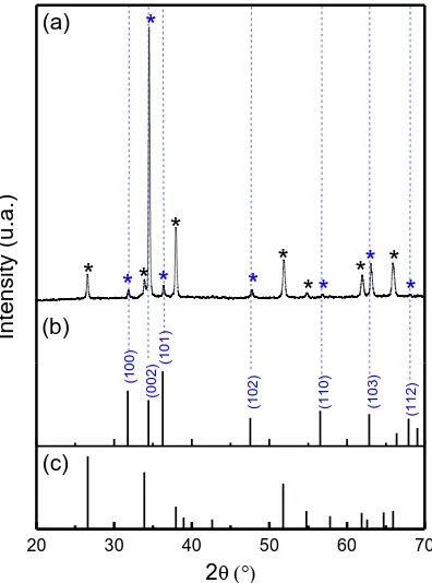
Figure 1 shows SEM images of a compact seed layer of ZnO grown by spin coating on the FTO surface and further covered with electrodeposited nanorods of the same oxide from a 2 mM Zn(NO3)2 solution at -0.9 V vs Ag/AgCl. It is observed that the array is highly oriented with an NR
the glass/FTO used as substrate (JCPDS, 41-1445, SnO2). A substantially high intensity is observed for
the (002) diffraction peak, indicating that the ZnO NR array grew along the c-axis normal to the substrate as shown in the SEM images.
Figure 1. SEM images from left to right: glass/FTO/ZnO seed layer; lateral view of ZnO NR arrays; top view.
Figure 2. (a) XRD pattern of ZNO NR arrays; (b) and (c) JCPDS of bulk ZnO and SnO2, respectively.
The band gap energy can be obtained by a linear fitting from the (h)2 vs. h plot, and the energy value corresponds to the intercept with the abscissa (Figure 3). This value is 3.38eV, which is very close to the expected room temperature band gap energy of bulk ZnO, which is between 3.2 and 3.4 eV at room temperature (22).
20 30 40 50 60 70
[image:4.596.95.503.148.251.2] [image:4.596.199.397.327.594.2]
Figure 3. (h)2 vs h plot. The intercept with the c axis is E
g.
The ZnO NR array was sensitized by the CH3NH3PbI3-x Clx perovskite as described in the
experimental section. The corresponding XRD pattern (Figure 4) exhibits reflection peaks at 2= 14.8° and 28.47°, which are associated with the (110) and (220) crystallographic perovskite planes (22), respectively.
Figure 4. XRD diffractogram of ZnO NRs covered with the CH3NH3PbI3-x Clx perovskite.
The sensitized ZnO NR structures were completed by adding a thin layer of spiro-MeTAD and other additives described in the experimental section. A gold contact was evaporated onto the top of the hole transport layer. Cell performance was evaluated by recording J/V curves under illumination equivalent to 1 sun (Figure 5). The device is characterized by a short-circuit (SC) current of 6.8 mA cm-2, open circuit voltage (OCV) of 0.85 V, a fill factor of 0.46 and a power conversion efficiency of
2.0 2.5 3.0 3.5 4.0
0 30 60 90
h(eV)
-ln
(T
)
*(
h
)
2
Eg=3.38 eV
0 10 20 30 40 50 60 70 80 90
0 1500 3000 4500 6000 7500 9000
Co
u
n
t
2 Theta
(110)
[image:5.596.126.468.403.622.2]
2.4%. In spite of the OCV being an acceptable value, the SC current and the fill factor are low compared to those recently reviewed for 1D ZnO NRs fabricated by hydrothermal methods and used in cells with CH3NH3PbI3 as absorber 23. Efficiency losses can originate from defects in the NR
morphology that may block the infiltration of the absorber but also from recombination at the surface and interfacial defects with the oxide, and between ZnO and the perovskite absorber 24, 25.
This low performance can be further improved by optimization of the different steps involved in the building of the cell architecture.
Figure 5. Current-voltage characteristics for glass/FTO/ZnO seed layer/ZnO NRs/CH3NH3PbI3-x Clx
spiro-OMeTAD/Au solar cell under 1 sun illumination.
4. CONCLUSIONS
Highly oriented ZnO NRs with c-axis preferred orientation were grown by electrodeposition on a ZnO seed layer and used as obtained for evaluating a solar cell based on CH3NH3PbI3-x Clx as an
absorber. The measured cell parameters under illumination of 1 sun were Voc= 0.85 V, JSC= 6.8 mA
cm-2 and a conversion efficiency of 2.4%. Further work is needed in order to improve these parameters, mainly to reduce charge transfer resistances at the interfaces between the electron transfer layer and the perovskite.
ACKNOWLEDGEMENTS
This work was supported by FONDECYT (Chile) and Dirección de Investigación, Pontificia Universidad Católica de Valparaíso Project 125. 702/215
References
1. J. Bursschka, N. Pellet, S. Jin Moon, R. Humphry-Baker, P. Gao. M.K. Nazeeruddin, M. Graetzel, Nature., 499 (2013) 316.
0.0 0.2 0.4 0.6 0.8
0 2 4 6 8
I
(
m
A
/
c
m
2 )
[image:6.596.172.417.219.406.2]
2. M.M. Lee, J. Teuscher, T. Miyasaka, T.N. Murakami, H.J. Snaith, Science., 338 (2012) 643. 3. J.M. Ball, M.M. Lee, A. Hey, H.J. Snaith, Energy Environ. Sci., 6 (2013) 1739.
4. M. Liu, M.B. Johnston, H.J.Snaith, Nature., 501 (2013) 395.
5. O.Malinkiewicz, A. Yella, Y.H. Lee, G.M. Espallargas, M. Graetzel, M.K. Nazeeruddin, H.J. Bolink, Nat. Photonics, 8 (2014) 128.
6. W. S. Yang, B-W. Park, E.H. Jung, N.J. Jeon, Y. C. Kim, D. U. Lee, S.S. Chin, S. J. SeO, E. K. Kim, J. H. Noh, S. I. Seok, Science., 356 (2017) 1376.
7. P.Qin, S. Tanaka, S. Ito, N. Tetrault, K. Manake, H. Nishino, M.K. Nazeeruddin, M. Gratzel, Nat. Commun. 5 (2014) 3834
8. P.V. Kamat, J.Am. Chem. Soc., 136 (2014) 3713.
9. Q. Chen, H. Zhou, Z. Hong, S. Luo, H.S. Duan, H.H. Yang, Y. Liu, G.Li, Y.Yang, J.Am. Chem. Soc., 136 (2014) 622.
10. H. J. Snaith, J. Phys. Chem. Lett., 4 (2013) 3623.
11. G.Giorgi, J. Fujisawa, H. Segawa, K. Yamashita, J. Phys. Chem. Lett., 4 (2013) 4213. 12. M. Liu, B. Johnson, H.J. Snaith, Nature., 499 (2013) 316.
13. M. Law, L.E. Green, J.C. Johnson, R. Saykally, P.D. Yang , Nat. Mater., 4 (2005) 455. 14. C. Magne, T. Moehl M. Urien, M. Gratzel, T. Pauporté, J. Mater. Chem. A, 1 (2013) 2079. 15. O. Lupan, V. M. Guerin, I.M. Tiginyanu, V.V. Ursaki, L. Chow, H. Henrich, T. Pauporté, J.Phys.
Chem. Lett., 4 (2010) 65.
16. J. Anta, E. Guillen, R. Tena-Zaera, J. Phys. Chem. C, 116 (2012) 11413. 17. D. Liu, T.L .Kelly, Nat. Photonics, 8 (2013) 133.
18. J. Y. Dong, J. Zhao, J. Shi; H.Wei, J. Xiao, X. Xu, D. Li, Y. Luo, Q. Meng, Chem. Commun., 50 (2014) 13381.
19. K. Mahmood, B.S. Swain, H.S. Jung, Nanoscale, 6 (2014) 9127.
20. C.D. Bojorge, V.R. Kent, E. Teliz, H.R. Canepa, R. Henriquez, H. Gómez, R.E. Marotti, E.A. Dalchiele, Physica Status Solidi A, 208 (2011) 1662.
21. C. Silvia, M. Edoardo, L. Andrea, G. Francesco, Chem. Mater., 25 (2013) 4613.
22. R.E. Marotti, P. Giorgi, G. Machado, E.A. Dalchiele, Sol. Energy Mat. Sol. Cells, 90 (2006) 2356. 23. P. Zhang, J. Wu, T. Zhang, Y. Wang, D. Lin, H. Chen, L. Li, C. Liu, W. Ahmad, Z. Chen, S. Li,
Adv. Mat., 30 (2018) 1703737.
24. D. Song, J. Im, H. Kim, N. Park, J. Phys. Chem. C, 118 (2014) 16567.
25. J. Dong, Y. Zhao, J. Shi, H. Wei, J. Xiao, X. Xu, J. Luo, J. Xu, D. Li, Y. Luo, Q. Meng, Chem. Commun., 50 (2014)13381