Int. J. Electrochem. Sci., 12 (2017) 3907 – 3915, doi: 10.20964/2017.05.51
International Journal of
ELECTROCHEMICAL
SCIENCE
www.electrochemsci.org
Short Communication
Effect of the Substrate Temperature on the Structural and
Morphological Properties of MoO
2Thin Films Obtained by
Pulsed Injection MOCVD
R. Narro-García1, N. Méndez2, L.M. Apátiga2, J.P. Flores-De los Ríos1, C.G. Nava-Dino1 and R. Quintero-Torres2,*
1
Universidad Autónoma de Chihuahua, Facultad de Ingeniería, Circuito Universitario S/N, 31125 Chihuahua, Chih., México
2
Centro de Física Aplicada y Tecnología Avanzada, Universidad Nacional Autónoma de México, Boulevard Juriquilla 3001, Querétaro 76230, México
*
E-mail: [email protected]
Received: 16 December 2016 / Accepted: 15 February 2017 / Published: 12 April 2017
Molybdenum oxides is of great technological interest due to their outstanding optical, electronic and catalytic properties. In this work, molybdenum dioxide (MoO2) thin films were deposited onto Si
wafers and stainless steel substrates at different substrate temperatures. The growth of the films was achieved by using a vertical metal organic chemical vapor deposition reactor working in pulsed injection mode. A powder of molybdenum hexacarbonyl mixed in a toluene solution was used as precursor. An effective pulsed injection system to supply the precursor, usually used for fuel injection in internal combustion devices, delivers a precise amount of liquid precursor to the reactor through injectors, whose pulse intervals (injection frequency) are controlled by a computer-driven system. The use of a liquid solution as precursor along with the experimental parameters provide thermodynamically favorable conditions to fabricate a thin solid film, homogenously deposited onto the whole substrate. The MoO2 film structure and morphology were studied by X-ray diffraction,
Raman scattering spectroscopy and scanning electron microscopy. Moreover, a comparative study was undertaken whereby the catalytic activity of stainless steel substrate for hydrogen evolution reaction was related to that of MoO2 thin film.
Keywords: MoO2 thin films; MOCVD; molybdenum oxides; catalytic activity
1. INTRODUCTION
of some metals [1-4], suggests that MoO2 can be used as an anode material for Dodecane-Fueled
solid-oxide fuel cells [5], partial oxidation of isooctane [6] and lithium ion batteries [7-10].
So far, several methods to grow MoO2 thin films have been explored including, sputtering
deposition [11-13], hot-filament metal oxide deposition [14], aerosol assisted chemical vapor deposition [15], electrodeposition [16, 17], electrostatic spray deposition [5] and epitaxial growth [18]. The structure, phase and properties of the resulting films are in general, strongly dependent upon the deposition technique employed.
In particular, the pulsed injection-metal organic chemical vapor deposition (PI-MOCVD) system is an attractive technique due to its excellent conformal coverage and low deposition temperatures. Moreover, the PI-MOCVD has the ability to cover large areas, high growth rates, step coverage possibility, and low cost [19-23]. A variety of metallic oxides have been produced using this system. However, the fabrication and characterization of MoO2 thin films by PI-MOCVD have not
been investigated yet.
In this study, we report the preparation of MoO2 thin films by PI-MOCVD. The structure and
morphology were studied by Raman, XRD, and SEM. A comparative study was undertaken whereby the catalytic activity of stainless steel substrate for hydrogen evolution reaction (HER) was compared to that of MoO2 thin film.
2. EXPERIMENTAL SECTION
The growth of the films was achieved using a vertical MOCVD reactor working in pulsed injection mode. The reactor consists of a quartz tube and stainless steel parts interconnected by O-rings producing a linear path from the gas carrier and injectors-end to the vacuum pump-end. The pulsed injection mechanism that consists of an injector normally used in internal combustion engines, allowed us to control the exact dose of liquid precursor into the reactor, where the injection frequency is controlled by a computer program. Once the precursor is injected, the liquid solution instantaneously evaporates and the resulting vapor mixture is transported by a carrier gas (N2) to the reaction chamber,
which is at high temperature, allowing the film growth on the hot substrate. The reaction chamber is a quartz tube surrounded by a resistance that can heat the substrate to 1000 °C. Circular stainless steel and rectangular silicon wafer with 1 cm diameter and 1.5 cm x 1 cm dimensions were used as substrates, respectively. The substrates were polished and cleaned prior to use by washing them with acetone and then ethanol in an ultrasonic bath for 10 min. Finally, substrates were dried in air.
A liquid solution of 30 ml of toluene mixed with 0.2139 gr of molybdenum hexacarbonyl (C6MoO6) was used as precursor. The pressure in the system was kept at 600 Pa with a flow of carrier
gas (N2) of 0.1 liters / min . Three experiments were performed by varying the substrate temperature at
500, 700 and 800 ºC, lower temperatures inhibits the material stoichiometry and the substrate coverage, the evaporation zone along the transport was kept at 280 ° C. The deposition parameters, substrates and sample labels are summarized in Table 1
the Cu radiation ( , an accelerating voltage of 40 kV and a current of 30 mA. The Raman signals were collected using a Sentera Dispersive Raman Microscope. The excitation laser wavelength and power were 785 nm and 25 mW, respectively.
The electrochemical test for hydrogen evolution activity was performed in a three-electrode cell arrangement using a thin platinum plate as the counter electrode, a saturated calomel electrode (SCE) as a reference electrode and the prepared samples as the working electrode. The voltage sweep potentials were provided by a computer controlled potentiostat/galvanostat (Princeton Applied Research, VersaSTAT 4 model). All the potentials described in the text were relative to the SCE. The linear polarization curves and electrochemical impedance spectroscopy (EIS) techniques were carried out in 0.5 M H2SO4 solution at room temperature. Before each experiment, the electrolyte solution
[image:3.596.47.551.354.438.2]was deaerated by bubbling nitrogen for 30 min, keeping an inert atmosphere during the whole measurement. The current density versus electrode potential curves were performed at a scanning rate of 10 mV/s. EIS measurements were carried out in the frequency range 1 to 105 Hz at overpotential (η=-450 mV) with the perturbation amplitude of 10 mV.
Table 1. Deposition parameters of PI-MOCVD process, substrate and corresponding sample label.
Sample Tsubstrate
(oC)
Tevaporation
(oC)
N2 flow rate
(l min-1)
Substrate
T500-Si 500 280 0.1 Silicon wafer
T700-Si 700 280 0.1 Silicon wafer
T800-Si 800 280 0.1 Silicon wafer
T800-SS 800 280 0.1 Stainless steel
3. RESULTS AND DISCUSSION
Figure 1 shows the Raman spectra of MoO2 films deposited at: 500 oC, 700 oC and 800 oC.
This range of temperature produced no change to the Raman spectra. All the Raman spectra are constituted by ten peaks located at 206, 229, 350, 364, 423, 468, 496, 569, 586, 743 cm-1, in good agreement with the spectrum of MoO2 previously reported by [24, 25]. No spectral evidence for
crystalline or amorphous MoO3 was observed due to the high substrate temperature.
Figure 2 shows the XRD pattern of MoO2 films deposited at different substrate temperatures of
500, 700 and 800 oC. In Figure 2 the obtained diffraction peaks at 2θ (o) are around 18.5, 26, 31.8, 37.02, 41.78, 49.56, 53.56, 60.3, 63.4, 66.6, 67.64, 70.02, 72.5, 73.36, 78.8, and 79.64. Unlike molybdenum oxide thin film prepared by MOCVD using molybdenum dioxide acetylacetonate as precursor in which the film consisted of α-MoO3 phase at deposition temperature of 560 oC [26], all
the identified peaks from the presented set of samples can be indexed to the monoclinic phase MoO2
(JCPDS card 32-0671) which is consistent with the Raman study. It is observed that the intensity of the sharp diffraction peak located at 2θ=26o increases with the substrate temperature which suggests that the thin film is well crystallized and exhibits the presence of MoO2 dominant phase with a strong
[image:4.596.100.497.127.415.2]
calculated lower value of crystallite size by using the well-known Debey–Scherrer’s formula gives and estimation of 40, 49 and 46 nm for samples deposited at 500 oC, 700 oC and 800 oC, respectively.
Figure 1. Raman spectra of the MoO2 films deposited at: 500 oC, 700 oC and 800 oC.
Figure 2. XRD pattern of the MoO2 films for different substrate temperatures of 500 °C, 700 °C and
[image:4.596.115.478.470.727.2]
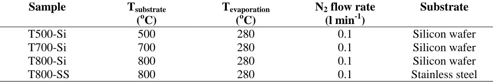
Scanning electron microscopy (SEM) was used to examine the surface morphology of the films and measure the film thickness. Error! Reference source not found.(a), (b) and (c) show the SEM images for the samples deposited at 500 oC, 700 oC and 800 oC. The microstructure of the deposited films changes depending on the substrate temperature. The SEM image for a sample deposited at low substrate temperature (T=500 oC) revealed nanostructured thin films with an average grain size of 38±7 nm while samples deposited at higher substrate temperatures exhibited an enhancement in the grain size, i.e. the average grain size of samples deposited at T=700 is 172±32 nm. The increase of the crystallite size corresponds to a coalescence of small crystallites as can be seen in Error! Reference source not found.(d) and this nanoparticle coalescence seems to be higher for samples deposited at 800 oC. It is worth to mention that this morphology differs greatly from that of a MoO2 thin film
obtained by aerosol assisted chemical vapor deposition at 500 oC [15] in which the coating is comprised of spherical and needle agglomerates of crystallites up to 1 μm. The film thickness of the samples is around 200 nm as measured by cleaving the sample and measuring in the SEM.
Figure 3. SEM images of MoO2 films for different substrate temperatures: a) T500-Si; b) T700-Si; c)
T800-Si; and d) show a different zone of sample deposited at 700 oC captured with a higher magnification (M=150k).
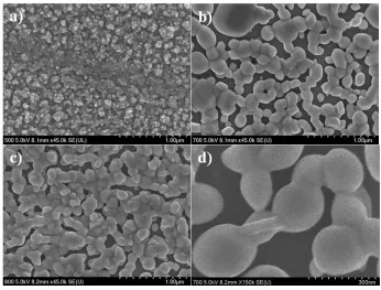
A comparative study was undertaken whereby the catalytic activity of stainless steel substrate for HER was related to that of MoO2 thin filmdeposited at 800 oC (T800-SS), this sample presented
the larges difference compared with the stainless steel substrate. Figure 4 shows the polarization curves for the stainless steel substrate and MoO2 coating. Current densities (j) were normalized to the
geometric area of the exposed surface. The catalytic property of the electrode for HER was significantly enhanced by the MoO2 thin film deposition onto the surface of the stainless steel. The
[image:5.596.124.470.318.581.2]
comparable to that shown by Y. Zhao et al. [27] showing the increase of HER with the addition of MoO2. The improved electrocatalysis exhibited by the MoO2 coating suggests that smaller activation
[image:6.596.107.490.137.407.2]energy is required for HER.
Figure 4. Linear sweep voltammetry polarization curves for the stainless steel substrate and the MoO2
thin film deposited at 800 oC onto stainless steel (T800-SS).
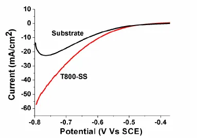
The EIS of the electrode is also an important parameter and can be used to evaluate the HER. Figure 5 shows the representative Nyquist plots of the stainless steel substrate and the MoO2 coating at
the overpotential -450 mV. The diameter of the semicircle is attributed to the interfacial charge transfer resistance of electrochemical reactions. The decrease of semicircle of Nyquist plots suggests an increase in the current density i.e. an increase in the rate of hydrogen evolution, attributed to the increase in the effective electrochemical interface by improved electron supply. This phenomenon facilitate the fast change transfer between the electrolyte and the MoO2 coating. Similar results are
shown in measurements made by B. W. Kwon et al. [5] where a reduction in the resistance of the cell is observed when working with MoO2. Both impedance curves reflect a distribution of reactivity that is
commonly fitted by using a simplified Randles equivalent circuit [28-30]. The equivalent electrical circuit consists of an active electrolyte resistance RS in series with the parallel combination of a
constant phase element (CPE) and an active charge transfer resistance Rct (see the inset of Figure 5). Its
impedance (Z) is described as:
(1)
where C is the CPE capacitance parameter and α is the CPE exponent. From the fitting parameters of the EIS data, Rs values are 6.5 Ω and 8 Ω for stainless steel substrate and T800-SS,
( )
1 ( )
ct s
ct R
Z R
i C R
respectively, manifesting excellent conductivity of electrolyte. Additionally, Rct decreases from 964
Ohm∙cm2
to 102 Ohm∙cm2 for stainless steel substrate and T800-SS, respectively (Table 2) all the values are for an area of 0.384 cm2. This suggests that MoO2 coating enhances the electrocatalytic
activity of the stainless steel substrate. Other work involving MoO2 coatings exhibits a reduction in Rct
values from 114 Ohm∙cm2
[image:7.596.112.485.222.505.2](uncoated) to 7 Ohm∙cm2 (coated) [5], validating the behavior obtained in the present work. The EIS results obtained are in reasonable agreement with those obtained from the linear polarization curves.
Figure 5. Electrochemical impedance spectra at η=-450 mV for sample T800-SS and substrate
Table 2. The kinetic parameters for substrate and T800-SS sample
Parameters Substrate M800-SS MoO2 coating [5]
RS (Ω∙cm2) 2.50 3.07 -
Rct (Ω∙cm2) 964 102 7
C (μF) 19 142 -
α 0.83 0.83 -
4. CONCLUSION
[image:7.596.43.560.590.662.2]
samples. The structure and morphology of the MoO2 thin films are highly dependent on the substrate
temperature. The thin films are well crystallized and exhibit the presence of MoO2 dominant phase
with a strong preferential orientation in (-1 1 1) direction for the highest substrate temperature (T=800
o
C). It was observed that the average grain size increases with substrate temperature from 40 nm to 200 nm approximately. It is worth to mention that this morphology differs greatly from that of MoO2 thin
films reported previously by other techniques. The catalytic properties of a MoO2 thin film were
evaluated using linear scan voltammetry and EIS. The results showed that the catalytic properties of the electrode for HER were significantly enhanced by the presence of MoO2 thin film deposition onto
the surface of the stainless steel.
ACKNOWLEDGMENTS
The authors would like to thank CONACYT for scholarship to N. Méndez. This research was possible thanks to the program UNAM-DGAPA-PAPIIT, Grant no. IN111614 and IN112017. The support of A. del Real, C. Peza, B. Millán and E.M Rivera is also gratefully acknowledged.
References
1. M. K. Trivedi, R. M. Tallapragada, A. Branton, D. Trivedi, G. Nayak, O. Latiyal, S. Jana, Int. J. Mater. Sci. Appl., 4 (2015) 354.
2. Y. Jin and P. K. Shen, J. Mater. Chem. A, 3 (2015) 20080.
3. N. Miyata, T. Suzuki and R. Ohyama, Thin Solid Films, 281–282 (1996) 218. 4. V. Bhosle, A. Tiwari and J. Narayan, J. Appl. Phys., 97 (2005) 083539.
5. B. W. Kwon, S. Hu, O. Marin-Flores, M. G. Norton, J. Kim, L. Scudiero, J. Breit and S. Ha, Energy Technol., 2 (2014) 425.
6. O. Marin-Flores, L. Scudiero and S. Ha, Surf. Sci., 603 (2009) 2327.
7. Y. Shi, B. Guo, S. A. Corr, Q. Shi, Y. Hu, K. R. Heier, L. Chen, R. Seshadri and G. D. Stucky, Nano Lett., 9 (2009) 4215.
8. H. Zhang, T. Wu, K. Wang, X. Wu, X. Chen, Y. Jiang, X. Wei and J. Chen, J. Mater. Chem. A, 1 (2013) 12038.
9. M. Sarno, A. Garamella, C. Cirillo and P. Ciambelli, Chem. Eng. Transac., 41 (2014) 307. 10.J. Hwang, D. Yoon, B. Kweon, W. Chang and J. Kim, RSC Adv., 6 (2016) 108298.
11.P. A. Spevack and N. S. McIntyre, J. Phys. Chem., 97 (1993) 11031.
12.M. Cano-Lara, S. Camacho-López, A. Esparza-García and M. A. Camacho-López, Opt. Mater., 33 (2011) 1648.
13.Y. Liu, H. Zhang, P. Ouyang, W. Chen, Y. Wang and Z. Li, J. Mater. Chem. A, 2 (2014) 4714. 14.M. A. Bica de Moraes, B. C. Trasferetti, F. P. Rouxinol, R. Landers, S. F. Durrant, J. Scarmínio
and A. Urbano, Chem. Mater., 16 (2004) 513.
15.S. Ashraf, C. S. Blackman, G. Hyett and I. P. Parkin, J. Mater. Chem., 16 (2006) 3575. 16.N. Dukstiene, D. Sinkeviciute and A. Guobiene, Cent. Eur. J. Chem., 10 (2012) 1106. 17.R. S. Patil, M. D. Uplane and P. S. Patil, Int. J. Electrochem. Sci., 3 (2008) 259. 18.E. Ahn, Y. Seo, J. Cho, I. Lee, J. Hwang and H. Jeen, RSC Adv., 6 (2016) 60704.
19.A. Abrutis, L. G. Hubert-Pfalzgraf, S. V. Pasko, A. Bartasyte, F. Weiss and V. Janickis, J. Cryst. Growth, 267 (2004) 529.
23.J. Crepelliere, P. L. Popa, N. Bahlawane, R. Leturcq, F. Werner, S. Siebentritt and D. Lenoble, J. Mater. Chem. C, 4 (2016) 4278.
24.P. A. Spevack and N. S. McIntyre, J. Phys. Chem., 96 (1992) 9029.
25.M. A. Camacho-López, L. Escobar-Alarcón, M. Picquart, R. Arroyo, G. Córdoba and E. Haro-Poniatowski, Opt. Mater., 33 (2011) 480.
26.R. M. Guerrero, J. R. V. Garcia, V. Santes and E. Gomez, J. Alloys Compd., 434–435 (2007) 701. 27.Y. Zhao, Y. Zhang, Z. Yang, Y. Yan and K. Sun, Sci. Technol. Adv. Mater., 14 (2013) 043501. 28.J. R. Macdonald, Impedance spectroscopy: Emphasizing solid materials and systems, John Wiley
and Sons, (1987) New York, USA.
29.M. E. Orazem and B. Tribollet, Electrochemical impedance spectroscopy, John Wiley and Sons, (2008) New Jersey, USA.
30.L. Quej-Aké, R. Cabrera-Sierra, E. Arce-Estrada and J. Marín-Cruz, Int. J. Electrochem. Sci., 3 (2008) 56.