Growth and Characterisation of InP
Nanowires and Nanowire-Based
Heterostructures for Future Optoelectronic
Device Applications
H. Aruni Fonseka
February 2015
A
THESIS SUBMITTED FOR THE DEGREE OFD
OCTOR OFP
HILOSOPHYOF
T
HEA
USTRALIANN
ATIONALU
NIVERSITYDepartment of Electronic Materials Engineering
Research School of Physics and Engineering
College of Physical and Mathematical Sciences
iii
Declaration
This thesis, to the best of my knowledge and belief, does not contain any results previously published by another person or submitted for a degree or diploma at any university except where due reference is made in the text.
H. Aruni Fonseka
Department of Electronic Materials Engineering, Research School of Physics and Engineering, College of Physical and Mathematical Sciences, The Australian National University,
Canberra, ACT 2601, Australia.
v
Acknowledgements
This thesis would not have become a reality without the direct or indirect contributions from many individuals and entities.
First of all, I would like to thank Prof. Chennupati Jagadish for giving me the opportunity to pursue this PhD. Jagadish has been an inspiring research leader and a great advisor, not only regarding matters related to my research, but also those related to my professional development. I am extremely grateful to my principal supervisor Prof. Hoe Tan for all the training and guidance he has given me in almost every aspect of research, from start to end. Hoe has been a very understanding supervisor during the good and the bad times. I consider myself very lucky to have had Hoe as my principal supervisor. I believe that Dr. Philippe Caroff’s arrival at the ANU was the biggest turning point of my PhD research. Philippe’s wealth of knowledge on nanowires is awe inspiring and his extreme passion for science has been contagious. I thank Philippe most sincerely for encouraging me when I was in need of it the most, and mentoring me every step of the way to reach this point. I am also very thankful to A/Prof. Jenny Wong-Leung who has taught and inspired me to carry out my research with attention to detail and thoroughness. I also wish to thank Drs. Michael Gao and Patrick Parkinson who have helped me in many ways with experimental setups or by sharing their immense knowledge in their respective fields.
Tom Kitchen, Dr. Kidane Belay, Josh Carr, Dane Kelly and Craig Saint are thanked for their help on numerous occasions.
Prof. Antonio Polimeni from the Sapienza Università di Roma, deserves a special note of acknowledgement. I am greatly in debt for the advice and guidance Antonio has provided, especially those related to photoluminescence spectroscopy, going beyond the capacity of a mere collaborator. Dr. Marta De Luca and Davide Tadeschi from the same institute are thanked for carrying out the tedious PL mapping measurements. In addition to Marta and Davide, Prof. Mario Capizzi, Attilio Zilli, Dr. Marco Felici from Sapienza Università di Roma, Prof. Thomas Nann and Tom Macdonald from University of South Australia, Prof. Sebastian Lourdudoss and Dr. Wondwosen Metaferia from KTH Sweden and everyone in the Nano Materials Physics group at University of Cincinnati are thanked for being great collaborators. I have greatly enjoyed working with them all and have learnt a lot on a number of diverse fields in the process.
I am grateful for the support of the entities and funding bodies who have contributed in making this research a reality. The Australian Research Council and the Government of Australia (Research Training Scheme) is acknowledged for the funding. The Australian Microscopy and Microanalysis Research Facility (AMMRF) and the Australian National Fabrication Facility (ANFF) which have been extensively used for the work in this thesis are sincerely thanked. The personnel in these facilities have made them enjoyable places to work in, even when the actual experiments were not going so well. Janet French-Wright and Josie Smith from the AMMRF, and Drs. Fouad Karouta, Kaushal Vora, Naeem Shahid from the ANFF are thanked for supporting me in various ways. I also wish to thank the EME and Vice-Chancellor’s travel grants for partly funding my travel costs to the MRS Fall conference in 2013. The RSPE stores, School Computer Unit, Electronics Workshop, School Facilities and all their staff including Goran Radovanovic, Patricio Romero, Benjamin Parker and Martin Conway are acknowledged for their help in many ways.
vii
including Drs. Jordan Kang, Filipe Kremer, Steffen Breuer, Shagufta Naureen, Suriati Paiman, Hannah Joyce, Dinesh Venkatachalam and Sudha Mokkapati. I also had the good fortune of meeting some of the best scientists in the world during this time and would like to especially thank A/Prof. Anna Fontcuberta i Morral from EPFL, Switzerland for the support and encouragement she has given me.
I had the privilege of sharing very good friendships with many of the past and present students at the EME. I wish to thank my best friend Amira Ameruddin once again for her friendship; my time at EME wouldn’t have been the same without her. My heartfelt gratitude goes to all my other good friends, Lachlan Smillie, Jenny Jiang, Tim Burgess, Dhruv Saxena, Keng Chan, Qian Gao, Huda Alkhaldi, Allina Nadzri, Fred Yuan, Kun Peng, Dr. Thomas Bierschenk, Dr. Daniel Pyke, Sarita Deshmukh, Vidya Ramesh, Bijun Zhao, Andy Feng, Sanjoy Nandi, Reddy Narangari, Haofeng Lu, and Dr. Ian McKerracher (among many others that may have momentarily slipped my memory), for sharing this journey with me. Having great friends like them around have certainly made these few years, some of the best in my life.
I should specially thank my family, my uncles, aunts, cousins and my two beautiful nieces for their company and keeping me sane during these few years. I thank my father, my very first physics teacher who inspired me to pursue science and my mother, for her unconditional love and understanding. Last, but certainly not least, I thank my husband, Dumidu, my rock and greatest strength, for being beside me throughout this journey.
ix
Abstract
Indium Phosphide (InP) forms a cornerstone amongst direct band-gap III-V compound semiconductors with the possibility for a wide range of other III-V alloys to be lattice matched with it. It is commonly used in optical communications related device applications, high electron mobility transistors (HEMTs) and heterojunction bipolar transistors (HBTs). The very low surface recombination velocity of InP has made its nanowire counterpart a standout amongst nanowires of other III-V materials with successful demonstrations in nanowire solar cells, lasers and single photon sources. Considerable progress has been made in terms of InP nanowire growth in the past decade. Defect-free wurtzite (WZ) phase nanowires with good optical quality have been achieved on InP (111)B substrates. However, there are unexplored areas related to nanowire heterostructures that may hold promise for future device applications. Furthermore, InP nanowires aimed for future integrated devices need to be grown on the Si (111) substrates, and preferably on Si (100) substrates, in order to be integrated with microelectronics and other planar devices on a single chip.
This dissertation presents a progressive advancement of Au seeded InP nanowire growth by MOVPE, from heterostructures grown on InP (111)B substrates to nanowire growth on Si (111) substrates and [100] oriented InP substrates. A number of diverse techniques have been employed to understand the growth process and characterise the samples. Scanning and transmission electron microscopy, atomic force microscopy, X-ray diffraction (XRD) and energy dispersive X-ray spectroscopy (EDX) have been used for structural and compositional analysis, while room and low temperature photoluminescence (PL) and PL mapping have been used for optical characterisation.
InP-InxGa1-xAs nanowire quantum wells (QWs) emitting in the 1.3 μm optical
communications wavelength region are grown on InP (111)B substrates. Detailed structural and optical analysis carried out using cross-sectional TEM (X-TEM) and PL mapping reveal asymmetric diffusion at the two interfaces of the QW, and broad, yet bright and homogenous PL emission along the complete length of the nanowire, with no emission visible from the InP nanowire core or outer barrier. The emission wavelength of the QW is tuned in the 1.3
μm range by varying the QW thickness as well as composition. The WZ phase QWs are
InP nanowire growth on Si (111) substrates has been carried out using an intermediate buffer layer. A two-step approach is used for the growth of the buffer layer and the growth parameters are optimised for both steps in order to achieve a smooth layer that covers the underlying Si substrate. It is seen that the layer fully relaxes by forming dislocations at the interface and is of (111)B polarity. Over 97% vertical nanowire yield is achieved on the buffer layers, and these nanowires are found to be similar in morphology and optical properties to those grown homoepitaxially on InP (111)B substrates under the same growth conditions.
InP nanowires grown on the industry standard [100] orientated substrates are examined by studying the growth directions, facets and crystal structure of the different types, namely, vertical, non-vertical and planar nanowires grown on InP (100) substrates. The seemingly random growth directions of the non-vertical nanowires are actually found to be <111> and <100> directions that acquire complex orientations with respect to the substrate due to the consecutive three dimensional twinning that takes place at the initial stages of growth. These directions are mathematically calculated and verified by the measurements carried out on individual nanowires. It is shown that 99% of the nanowires grown on InP (100) substrate are either <100>, <111> or <110> oriented with growth facets of either {100} or {111}.
The relative yields of each type of nanowire grown on InP (100) substrates are controlled by optimising the pre-growth annealing and growth conditions. A maximum of 87%, 100% and 67% yield is achieved for vertical, planar and non-vertical nanowires, respectively. The novel families of side facets of <100> nanowires are engineered to obtain cross-sectional shapes ranging from square to octagonal while maintaining a high vertical yield. Growth parameters and post-growth in-situ annealing conditions are tuned in order to achieve this. Finally, InGaAs QWs are grown on a novel and asymmetric facet combination of [100] nanowires, demonstrating the intended non-uniform complex growth that results in different thicknesses and compositions on the different types of nanowire facets.
xi
Publications
Journal Articles
1. H. A. Fonseka, H. H. Tan, J. Wong-Leung, J. H. Kang, P. Parkinson and C. Jagadish, “High vertical yield InP nanowire growth on Si(111) using a thin buffer layer”, Nanotechnology, vol. 24, no. 46, p. 465602, 2013.
2. H. A. Fonseka, P. Caroff, J. Wong-Leung, A. S. Ameruddin, H. H. Tan, and C. Jagadish, “Nanowires grown on InP (100): Growth directions, facets, crystal structures, and relative yield control”,ACS Nano, vol. 8, no. 7, pp. 6945-6954, 2014.
3. M. De Luca, A. Polimeni, H. A. Fonseka, A. J. Meaney, P. C. M. Christianen, J. C. Maan, S. Paiman, H. H. Tan, F. Mura, C. Jagadish, and M. Capizzi, “Magneto-optical properties of wurtzite-phase InP nanowires”, Nano Letters, vol. 14 , no. 8, pp. 4250-4256, 2014.
4. M. De Luca, A. Zilli, H. A. Fonseka, S. Mokkapati, A. Miriametro, H. H. Tan, L. M. Smith, C. Jagadish, M. Capizzi, and A. Polimeni, “Polarized light absorption in wurtzite InP nanowire ensembles”, Nano Letters, in press, doi:10.1021/nl5038374.
5. A. Zilli, M. De Luca, D. Tedeschi, H. A. Fonseka, A. Miriametro, H. H. Tan, C. Jagadish, M. Capizzi and A. Polimeni, “Temperature dependence of interband transitions in wurtzite InP nanowires”, ACS Nano, in review.
6. A. S. Ameruddin, H. A. Fonseka, P. Caroff, J. Wong-Leung, R. L. M. Op het Veld, J. L. Boland, M. B. Johnston, H. H. Tan, and C. Jagadish, “InxGa1-xAs nanowires
Conference Papers
1. H. A. Fonseka, H. H. Tan, J. H. Kang, S. Paiman, Q. Gao, P. Parkinson, C. Jagadish, “Growth of InP nanowires on silicon using a thin buffer layer”, in 2012 Conference on Optoelectronic and Microelectronic Materials & Devices (COMMAD), Melbourne, VIC, Australia, 12-14 Dec. 2012, pp.43-44, 2012.
2. A. S. Ameruddin, H. H. Tan, H. A. Fonseka, Q. Gao, J. Wong-Leung, P. Parkinson, S. Breuer, C. Jagadish, “Influence of growth temperature and V/III ratio on Au-assisted InxGa1−xAs nanowires”, in 2012 Conference on Optoelectronic and
Microelectronic Materials & Devices (COMMAD), Melbourne, VIC, Australia, 12-14 Dec. 2012, pp.37-38, 2012.
xiii
Acronyms and Symbols
a.u arbitrary units
AFM atomic force microscopy
As arsenic
AsH3 arsine
Au gold
Avg average
BSE back scattered electrons
DI deionised
DOS density of states
EDX energy dispersive X-ray spectroscopy FWHM full width at half maximum
Ga gallium
HAADF high angle annular dark field
In indium
MOVPE metal organic vapour phase epitaxy MQW multiple quantum well
NP nanoparticle
NW nanowire
P phosphorous
PH3 phosphine
PL photoluminescence
QW quantum well QWR quantum wire QWT quantum well tube RMS root mean square RSM reciprocal space map RT room temperature
SADP selected area diffraction pattern SE secondary electron
SEM scanning electron microscopy SF stacking fault
Si silicon
SQW single quantum well
STEM scanning transmission electron microscopy TEM transmission electron microscopy
TMGa trimethylgallium TMIn trimethylindium VLS vapour-liquid-solid VS vapour-solid
WZ wurtzite
XRD X-ray diffraction X-SEM cross-section SEM X-TEM cross-section TEM
xv
Contents
Declaration ... iii
Acknowledgements ... v
Abstract ... ... ix
Publications ... xi
Acronyms and Symbols ... ... xiii
Contents . ...xv
List of Figures ... xix
List of Tables ... xxiii
Chapter 1: Introduction ... 1
1.1 InP Semiconducting Material ... 1
1.2 InP in Nanowire Form ... 3
1.2.1 Demonstrated Applications of InP Nanowires ... 3
1.2.2 Progress Made So Far in Relation to InP Nanowire Growth ... 4
1.2.3 Areas That Require Further Investigation in Relation to InP Nanowire Growth for Future Optoelectronic Devices and Associated Challenges ... 5
1.3 Thesis Synopsis ... 7
1.4 References ... 8
Chapter 2: Basic Concepts Related to Nanowires ...17
2.1 Formation of Stacking Faults and WZ Phase in <111> Oriented Nanowires ...17
2.2 Defect-Free ZB Phase Nanowire Growth in <100> Directions ...19
2.3 Polarity of Facets in Compound Semiconductors ...20
2.4 Common Low-Index Side Facet Combinations and Cross-Sectional Shapes of Conventional [111] Oriented Nanowires ...21
2.5 Growth of Lattice Mismatched Nanowire Based Structures ...23
2.6 Direct and Indirect Band-Gaps of Semiconductors ...25
2.8 Quantum Confinement and Nanowire-Based Quantum Heterostructures ... 27
2.9 Summary ... 29
2.10 References ... 29
Chapter 3: Experimental Techniques ... 33
3.1 Metal Organic Vapour Phase Epitaxy (MOVPE)... 33
3.1.1 Vapour-Solid (VS) Growth in MOVPE ... 34
3.1.2 Vapour-Liquid-Solid (VLS) Growth in MOVPE ... 35
3.1.3 Sample Preparation for Nanowire Growth ... 37
3.2 Electron Microscopy... 37
3.2.1 Scanning Electron Microscopy (SEM) ... 38
3.2.2 Transmission Electron Microscopy (TEM) ... 40
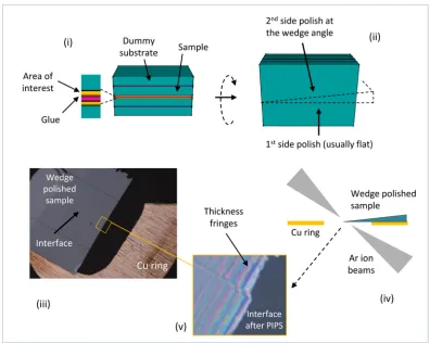
3.3 Sample Preparation for TEM ... 43
3.3.1 Sample Preparation for Determination of Crystal Structure and Defect Densities of Nanowires using the Side View ... 44
3.3.2 Cross-section Sample Preparation of Layers, Planar Nanowires, Nano-Particles Embedded in the Substrate and Nanowires in the Early Stages of Growth using Tripod Polishing ... 44
3.3.3 Lateral Cross-Section Preparation of Nanowires using Microtome Sectioning ... 46
3.4 Energy Dispersive X-ray Spectroscopy (EDX) ... 47
3.5 X-ray Diffraction (XRD) ... 48
3.6 Atomic Force Microscope (AFM) ... 50
3.7 Photoluminescence (PL) Spectroscopy... 51
3.8 Summary ... 53
3.9 References ... 53
Chapter 4: InP-InxGa1-xAs Core-Multi-Shell Nanowire Quantum Wells Emitting in the 1.3 μm Wavelength Range ... 57
4.1 Introduction ... 57
4.2 Experimental Methods ... 58
4.3 Single Quantum Well Nanowires ... 59
4.4 Tunability of Nanowire Single Quantum Wells ... 65
4.4.1 Tunability by Variation of Quantum Well Thickness ... 65
4.4.2 Tunability by Variation of Quantum Well Composition ... 68
4.5 Multiple Quantum Wells... 70
4.6 Summary ... 72
xvii
Chapter 5: High Vertical Yield InP Nanowire Growth on Si (111) Using a Thin
Buffer Layer for Integration with Si Technology ...81
5.1 Introduction ...81
5.2 Experimental Methods ...83
5.3 Buffer Layer ...84
5.3.1 Initial Layer Growth ...84
5.3.2 Second Layer Growth...86
5.4 Nanowires ...91
5.5 Summary ...94
5.6 References ...94
Chapter 6: Nanowires Grown on (100) InP Substrates: Growth Directions, Facets and Crystal Structures ...99
6.1 Introduction ...99
6.2 Experimental Methods ... 100
6.3 Main Types of Nanowires Grown on InP (100) Substrate ... 101
6.3.1 Vertical Nanowires ... 101
6.3.2 Non-Vertical Nanowires ... 105
6.3.3 Planar Nanowires ... 116
6.4 Summary ... 119
6.5 References ... 120
Chapter 7: Relative Yield Control and Side Facet Engineering of InP Nanowires Grown on InP (100) Substrates for Complex Heterostructures... 123
7.1 Introduction ... 123
7.2 Experimental Methods ... 125
7.3 Variation of Relative Yields with Basic Growth Parameters ... 126
7.3.1 Effect of Growth Temperature ... 126
7.3.2 Effect of V/III Ratio and TMIn Flow Rate ... 127
7.4 Effect of Pre-Growth Annealing Conditions on the Relative Yields ... 129
7.4.1 Effect of Pre-Growth Annealing Temperature... 129
7.4.2 Effect of PH3 Flow Rate During Pre-Growth Annealing ... 129
7.5 Initial Stages of Formation of Different Types of Nanowires ... 131
7.6 Engineering the Side Facets of <100> Oriented Nanowires ... 133
7.6.1 Facet Engineering by TMIn Flow Rate Variation ... 136
7.6.2 Facet Engineering by in-situ Post Growth Annealing ... 137
7.8 Summary ... 144
7.9 References ... 145
Chapter 8: Conclusions and Future Research Directions... 151
8.1 Conclusions ... 151
8.2 Future Research Directions ... 154
8.2.1 Theoretical Modelling and Understanding of the Vertical Nanowire Nucleation on (100) Substrates ... 154
8.2.2 Investigating Other Complex Heterostructures Grown on [100] Oriented Nanowires and Their Applications... 155
8.2.3 High Vertical Yield InP Nanowire Growth on Si (100) Substrates ... 157
xix
List of Figures
Figure 1.1: Band-gap/wavelength against the lattice parameter of some common
semiconducting materials. ... 2
Figure 2.1: Crystal structure and formation of stacking faults in <111> oriented nanowires...18
Figure 2.2: Layer-by-layer stacking in [100] oriented nanowires ...19
Figure 2.3: Polarity of facets in compound semiconductors. ...20
Figure 2.4: ZB and WZ relative directions on the (111) surface and nano-facet formation on the major side facets of highly tapered nanowires. ...23
Figure 2.5: Illustration of growth of lattice-mismatched planar and nanowire- based structures. ...24
Figure 2.6: Band structures of ZB InP and Si...25
Figure 2.7: Band structures of ZB and WZ InP. ...26
Figure 2.8: Quantum confinement and nanowire-based quanum heterostructures. ...28
Figure 3.1: A schematic of the Aixtron 200/4 MOVPE reactor system. ...34
Figure 3.2: Adatom absorption and diffusion on planar surfaces and nanowire side walls. ...35
Figure 3.3: VLS growth process of nanowires. ...36
Figure 3.4: Signals produced by interaction of high-kV electrons with a sample. ...38
Figure 3.5: Interaction of electron beam with the sample in SEM. ...39
Figure 3.6: Ray diagrams of TEM in diffraction and imaging modes. ...40
Figure 3.7: Schematic of HAADF imaging in STEM mode. ...43
Figure 3.8: Process of TEM sample preparation using tripod polishing. ...45
Figure 3.9: Process of nanowire cross-section preparation using microtome sectioning...46
Figure 3.11: XRD analysis of palnar heterostructures. ... 49
Figure 3.12: Schematic illustration of AFM system and its capabilities. ... 50
Figure 3.13: Process of PL emission and Schematic of the PL system set-up. ... 51
Figure 4.1: Structural characterisation of nominally 7 nm thick In0.6Ga0.4As QW ... 60
Figure 4.2: Optical characterisation of single QWs... 62
Figure 4.3: Stacking fault distribution along the nanowire QW... 64
Figure 4.4: Tunability of QW emission by varying thicknes. ... 66
Figure 4.5: Tunability of QW emission by varying QW composition. ... 69
Figure 4.6: Optical characterisation of the MQW nanowires... 71
Figure 5.1: Effect of growth temperature on the initial InP layer grown on Si. ... 84
Figure 5.2: Effect of V/III ratio on the initial InP layer grown on Si. ... 85
Figure 5.3: Effect of growth temperature, V/III ratio and post-growth annealing on the second InP layer grown on Si... 87
Figure 5.4: TEM anaysis of the crystal structure of the InP buffer layer grown on Si. ... 88
Figure 5.5: XRD anaysis of the InP buffer layer grown on Si. ... 90
Figure 5.6: Polarity of the InP buffer layer grown on Si. ... 91
Figure 5.7: SEM images and PL spectra of the nanowires grown on InP and Si substrates, and buffer layers. ... 92
Figure 6.1: Types of nanowires that grow on InP (100) substrates and facets of the vertical nanowires ... 102
Figure 6.2: Formation of partially polar surfaces on the {011} nanowire facets with tapering. ... 103
Figure 6.3: The two types of non-vertical nanowires observed on the InP (100) substrates. ... 106
Figure 6.4: An atomistic model showing the possible 1st and 2nd order twinned <111> growth directions ... 106
Figure 6.5: Projections of the nanowire on the x, y, z axis system on (100) substrate. ... 108
Figure 6.6: Crystal structure and facets of <111> non-vertical nanowires. ... 111
Figure 6.7: Non-vertical <100> nanowire growth directions. ... 112
xxi
Figure 6.9: Morphology, growth directions, crystal structure and facets of
planar nanowires. ... 116
Figure 6.10: Layer by layer stacking in planar nanowires. ... 118
Figure 7.1: Effect of growth temperature on the relative yields. ... 126
Figure 7.2: Effect of V/III ratio and TMIn flow rate on the relative yields. ... 127
Figure 7.3: Effect of pre-growth annealing temperature on the relative yields. ... 128
Figure 7.4: Effect of PH3 flow rate duringpre-growth annealing on the relative yields ... 129
Figure 7.5: Initial stages of formation of different types of nanowires. ... 132
Figure 7.6: Variation of the side facets of the <100> oriented nanowires with the basic growth parameters ... 134
Figure 7.7: Variation of the morphology side facets of the <100> oriented nanowires with the TMIn flow rate. ... 137
Figure 7.8: Facet evolution of <100> nanowires with post-growth in-situ annealing ... 139
Figure 7.9: Structural characterisation of QWs grown on [100] nanowires with asymmetric facets... 141
Figure 7.10: Optical characterisation of QWs grown on [100] nanowires with asymmetric facet. ... 143
Figure 8.1: Initial stages of vertical nanowire growth on InP (100) substrates. ... 154
Figure 8.2: Possible novel structures based on [100] oriented nanowires. ... 156
xxiii
List of Tables
Table 1.1: Some key material parameters of InP compared with other common
semiconductors. . ... 2 Table 2.1: Common low-index facet combinations and cross sectional shapes of
[111] oriented nanowires. ...22 Table 2.2: Reported experimental and theoretical values of some key parameters
related to WZ InP band structure at the point.. ...27 Table 3.1: Typical ion beam energy values used in the PIPS.. ...45 Table 4.1: WZ InP, GaAs and InAs material parameters used for QW emission
wavelength simulation. ...68 Table 6.1: Possible low index facet combinations and cross sectional shapes for
vertical nanowires on (100) substrates. ... 104 Table 6.2: Growth directions of 3-dimensional twinned <111> nanowires grown
on InP (100) substrates up to the 3rd order. ... 109 Table 6.3: Growth directions of 3-dimensional twinned <100> nanowires grown
on InP (100) substrates up to the 3rd order. ... 114 Table 6.4: Summary of growth directions, facets and crystal structure of nanowires
grown on InP (100) substrates. ... 119 Table 7.1: Pre-growth annealing and growth parameters of the defined standard
sample ... 125 Table 7.2: Summary of pre-growth annealing conditions and growth parameters
to achieve high yields of different types of nanowires... 130 Table 7.3: Pre-growth and growth parameters for high vertical yield <100>
nanowires with {011} facets. ... 136 Table 7.4: Summary of pre-growth, growth and post growth anneal parameters
in order to achieve different facet profiles on <100> nanowires while
maintaining high vertical yield. ... 138
1
Chapter 1
Introduction
1.1
InP Semiconducting Material
InP is a commonly used III-V compound semiconductor that has a direct band-gap. The two common group IV elemental semiconductors, Si and Ge, have indirect band-gaps. This leads to lower radiative recombination efficiencies. Therefore, direct band-gap is one of the main advantages of most III-V compound semiconductors that are formed by combining elements from the groups on the either sides of the group IV in the periodic table. Band structures of semiconductors will be discussed further in Chapter 2.6 and 2.7.
However, the key property of InP, which makes it a stand-out amongst other direct band-gap III-V compound semiconductors is its lattice parameter. As seen in Figure 1.1, InP can be lattice matched with a wide range of other ternary and quaternary semiconducting materials that have a range of band-gaps and band alignment types with InP (note that only some key possible combinations are shown in Figure 1.1 for clarity). For example, lattice matched InAlAs has a higher band-gap than InP, while InGaAs has a lower band-gap [1]. This gives enormous freedom in designing InP-based heterostructures. While most materials show type I band alignment with InP, materials such as lattice matched GaAsSb shows type II band alignment with InP [2, 3]. The possibility to lattice match with InGaAsP and
InGaAs, that can be tuned to emit in the 1.3 and 1.55 μm optical communication wavelength
regions makes InP indispensable in photonic devices such as photodetectors, laser diodes, modulators, light emitting diodes and waveguides that are used in communication systems [4-14]. Optical communication related applications in fact, are the most popular type of thin film-based application that uses InP [15].
Figure 1.1: Band-gap/wavelength against the lattice parameter of some common semiconducting materials, adapted from [21]. The region shaded in grey indicates the lattice parameter range within ±1% of InP.
The value of the band-gap of InP, which is 1.35 eV at 300 K, is also advantageous for many applications. Solar cell is one of these and the band-gap in this region ensures high energy conversion efficiency [15]. Solar cells have been fabricated by combining other lattice matched materials as well as by only using InP doped layers [22-25]. High resistivity against radiation makes InP solar cells the best suited for space satellites [23, 26, 27]. The relatively high optical absorption coefficient also contributes to the success of InP solar cells [28, 29]. In the recent years, InP solar cells have been more successful in nanowire form [29-33]. This will be discussed in detail in the following section. In addition, lower surface recombination velocity which enhances minority carrier lifetimes and higher thermal conductivity which helps in power dissipation in electronic devices make InP a much favoured semiconductor [16, 34, 35].
Table 1.1 gives reported values of some of the above discussed material parameters (at 300 K), for InP, compared with other common semiconductors.
Parameter Si InP GaAs InAs
Lattice parameter (A) 5.431 5.8687 5.65325 6.0583
Band-gap (eV) 1.12
(indirect)
1.344 (direct)
1.424 (direct)
0.354 (direct) Intrinsic Carrier concentration (cm-3) 1×10¹⁰ 1.3×10⁷ 2.1×10⁶ 1×10¹⁵ Electron mobility (cm2 V-1s-1) ≤1400 ≤5400 ≤8500 ≤40,000 Hole mobility (cm2 V-1s-1) ≤450 ≤200 ≤400 ≤500 Thermal conductivity (W cm-1°C-1) 1.3 0.68 0.55 0.27
3
1.2
InP in Nanowire Form
The nanowire geometry brings in a number of advantages of its own. Orders of magnitude lower material usage, smaller device print, very high surface area (relative to the foot-print and material volume), ability to tolerate higher level of strain without forming dislocations [36, 37] and freedom to form heterostructures in all three dimensions are some of them [38]. In addition to these, ensembles of nanowires behave as highly efficient light absorbers, trapping the incident light within the ensemble [39-42]. It has been shown that carefully designed InP nanowire arrays could absorb 94% of the incident light with energy above the band-gap [42]. Semiconductor nanowires could be used on their own, like in lasers [43-45], as templates to grow heterostructures and cavities [38, 46] or as building blocks to grow more complex structures [47]. They have not only been used in devices, but during the past decade, nanowires have also been instrumental in a number of key fundamental scientific discoveries [48, 49].
In nanowire form, the very low surface recombination velocity of InP makes it a standout. As the high surface-to-volume ratio is inherent in nanowire geometry, fast surface recombination would be undesirable in many applications [50, 51]. Furthermore, the thin native oxide of InP, that is normally formed when exposed to air is stable under operating conditions of most devices [52]. These two properties eliminate the need for additional passivation or cap layers to be grown on InP nanowires in order to enhance radiative recombination or prevent degradation, in contrast to GaAs and AlGaAs. Again, similar to the planar case, InP nanowires can be integrated with a large range of binary and ternary materials in axial and radial heterostructures. It should be noted here, due to the possibility of strain relaxation in the radial and axial directions (to a lesser extent) the range of materials with different lattice constants that can be grown without defects, is further expanded than in the planar case [36, 37, 53-56].
1.2.1
Demonstrated Applications of InP Nanowires
InP nanowire solar cells [29-33] warrant a special mention. The three most recent reports [30, 32, 33] demonstrated close to or over 10% efficiency and that demonstrated in ref [33] is the highest reported efficiency for an array based nanowire solar cell [66]. This InP nanowire solar cell not only exceeded the ray optic limit by five times but also recorded the highest open-circuit voltage of 0.906 V, surpassing that of the best planar InP solar cell [67]. In addition to the above-mentioned characteristics, the high optical absorption coefficient [28], the band-gap of InP (which allows optimum absorption of the visible and near-infra red wavelengths where solar irradiance is also high) and the possibility to control the unnecessary parasitic layer and radial growth by in situ HCl etching [31, 68] have contributed to the success of InP nanowires in solar cell applications [29, 33]. Apart from the above, very recently, InP nanowires have been utilised in novel applications like water splitting [69] and hard x-ray detection [70].
1.2.2
Progress Made So Far in Relation to InP Nanowire Growth
Before proceeding to the discussion on the advances in growth, it is worth noting that arsenide and phosphide nanowires can grow in both zincblende (ZB) and hexagonal wurtzite (WZ) phases with controllable amounts of stacking defects, tuneable up to perfect structural quality. This is facilitated by the stacking sequence of ZB in <111> direction and will be further discussed in detail in Chapter 2.1. In the case of metal seeded VLS grown nanowires, the formation of a bilayer of a particular phase is governed by the interfacial energies between the particle, nanowire and the vapour phase [71]. InP has the lowest stacking fault energy out of all the common arsenide and phosphide III-V materials [72, 73]. This makes achieving pure crystal phase InP nanowires challenging as the phase could switch from one to another with small fluctuations in energy.
Resulting planar defects (twins in ZB and stacking faults in WZ) or mixed phase are not always detrimental. In fact, it could be seen from some of the above applications that they have not adversely affected the device, and in certain cases have even enhanced the device performance [44, 45, 59]. Stacking faults are even known to improve the mechanical properties of the nanowires [74]. On the other hand, in some applications, for example in single photon sources, phase purity is a must in order to maintain coherence for a longer time [64, 75].
5
nanowires for smaller Au particle sizes by increasing the V/III ratio [78]. Au seeded defect-free WZ InP nanowires have also been demonstrated using chemical beam epitaxy (CBE) [64, 79]. Naji et al. have demonstrated defect-free WZ InP nanowires growth by molecular beam epitaxy (MBE) on SrTiO3 (001) substrates [80].
Success has been much less in terms of achieving defect-free ZB InP nanowires. The highest level of control achieved up to date is the twinning superlattices, where the ZB structure is twinned periodically along the length of the nanowire. These have been achieved either by using large Au particles for the same high temperature growth conditions as pure WZ (and etching with HCl during growth) [77] or by doping with Zn [81].
In terms of optical properties, clean emission, limited to the free exciton and donor bound exciton transitions had been achieved for the MOVPE grown WZ InP nanowires by Vu et al., after the piranha cleaning of the nanowire side walls [77]. Similarly, after piranha etch, acceptor related emission have almost disappeared in the ZB superlattice nanowire spectra displaying clean free exciton emission with a 2.5 meV narrow line-width at 4 K [77]. Long carrier lifetimes between 1 to 3 ns have been observed for these WZ and ZB nanowires for excitation powers between 64 nJ pulse-1and 21 μJ pulse-1 at 4 K [77]. It should be noted that these optical properties have been measured without any passivation or shell growth around the InP nanowires.
1.2.3
Areas That Require Further Investigation in Relation to InP
Nanowire Growth for Future Optoelectronic Devices and
Associated Challenges
Almost all nanowires discussed so far have been grown homoepitaxially on InP (111)B substrates. It could be seen that considerable progress has been made and InP nanowire growth on InP (111)B substrates has almost reached its maturity in terms of growth, although there is plenty of room for exploration in terms of devices and applications.
However, if InP nanowires are to be integrated with well established Si technology so that complete, functional components can be designed on a single chip, they will have to be grown on Si substrates. Ideally, nanowires grown on Si substrates have to be of the same quality as those successfully demonstrated in above applications on InP (111)B substrates.
mid-gap states in Si and hence, Au seeded nanowires that are directly grown on Si would not be a viable choice for future device applications [89].
Self-catalysed InP nanowires have been successfully grown on Si with 100% vertical yield by one group [90]. The small growth parameter space has been the limiting factor in this case. Thus, there are only very limited options for crystal and optical quality improvement and tuning.
Looking further into the future, it is known that the Si technology has actually evolved on Si (100) substrates and nanowires are almost the only type of basic structure that is grown on substrates with a different orientation. Therefore, in the long term, to complete the integration on a commercially viable level, the ultimate requirement would be for the nanowires to be grown on Si (100) substrates. This change of substrate orientation changes many aspects of nanowire growth from the well-known (111) substrates. Vertical growth on these substrates is a challenge for a start, as the preferred low energy directions would still be <111> [91-94]. The parameters space for the nanowire growth on [100] direction would be different and special care, in the form of pre-growth treatment or otherwise, will have to be taken in order to change the growth direction to the energetically unfavourable [100] direction [95-97].
Therefore, it is clear that growth on Si(100) would require a completely new knowledge base. However, hardly any research has been carried out on homoepitaxial vertical nanowire growth on any III-V (100) substrates (up until recently), let alone on Si(100). The properties such as facets and crystal structures of nanowires grown in a different direction would also be different. This in fact is more of an opportunity as opposed to a challenge. As discussed in Chapter 2.4, [111] oriented nanowires could have a limited range of facet profiles depending on growth parameters. Likewise, the [100] orientation would give rise to a different set of profiles that cannot be accessed by conventional [111] nanowires. Even the <111> and other growth directions observed on the (100) substrates could be looked at from a novel point of view to create unique nanowire-based ensemble structures [47, 98].
7
Moving on to InP-related nanowire heterostructures, it could be seen that the focus has mainly been on only two materials, InAs and InAsP [53, 58, 62-64, 100-103]. The range of materials explored can be expanded to include other ternary and quaternary materials, especially the vast range that can be lattice matched as shown in Figure 1.1. III-V alloys such as InGaAs, InAlAs, GaAsSb and InGaAsP are some of such materials that allow band-gap variation over a wide range while maintaining a low lattice mismatch with InP. As mentioned earlier, in contrast to the planar case, reports on nanowire heterostructures targeting device applications in optical communications are relatively sparse [100]. Hence, there is plenty of room to investigate the nanowire counterparts of structures that have been well studied in the planar form and explore possibilities of incorporating the inherent advantages of the nanowire geometry in optical communications related applications.
1.3
Thesis Synopsis
This thesis presents a gradual advancement of growth of Au-seeded InP nanowires by MOVPE, in order to suit possible requirements for future optoelectronic device applications. It has investigated the progression from potential unexplored areas in growth on conventional InP (111)B substrates to growth on Si and finally, change of substrate orientation to suit industry standard [100]. Before proceeding to the main contributions, some relevant concepts related to nanowires are introduced in Chapter 2. A number of characterisation techniques have been used for the work presented in this dissertation and they are introduced in Chapter 3.
InP-InxGa1-xAs-InP radial quantum wells (QWs) emitting in the 1.3 μm wavelength
range that are grown on InP (111)B substrates are investigated in Chapter 4. The QW tube structures are structurally and optically analysed using X-TEM, micro-PL and PL mapping. The QW emission is tuned in the 1.3 μm region by varying the QW thickness as well as composition. The optical behaviour of the nanowire QWs are modelled using the 8-band kp model. Multiple quantum wells are also grown, demonstrating the potential to grow more complex structures.
Chapter 6 proceeds to investigate the nanowire growth on InP (100) substrates, which is an unconventional orientation for nanowire growth. As mentioned previously, nanowires do not easily grow vertically on these substrates and the resulting nanowires generally seem random. This chapter classifies these nanowires into three types, namely vertical, non-vertical and planar, and investigates the growth directions, facets and the crystal structures of each type in detail. The non-vertical nanowires are found to be <111> and <100> oriented nanowires that inherit complex growth direction with respect to the substrate due to the 3-dimensional twinning that takes place during the initial stages. The growth directions with respect to the substrate are calculated using a mathematical model and verified by the measurements carried out on a large number of single nanowires.
The knowledge gained in Chapter 6 is used in Chapter 7 to control the relative yields of the vertical, non-vertical and planar nanowires. Growth parameters and pre-growth annealing conditions are tuned to achieve 87%, 67% and 100% of vertical, non-vertical and planar nanowires, respectively. The side facets of the <100> oriented nanowires are engineered to form a range of facet profiles from square to octagonal cross-section shapes by tailoring the growth parameters and post-growth in situ annealing conditions. This is achieved while maximising the yield of vertical nanowires. Finally, the complex facets of [100] nanowires are used to demonstrate their potential for novel opto-electronic applications by growing InGaAs QWs on them.
Finally, Chapter 8 discusses the overall conclusions of this work and suggests possible future research directions.
1.4
References
[1]. D. K. Gaskill, N. Bottka, L. Aina and M. Mattingly, "Band‐gap determination by photoreflectance of InGaAs and InAlAs lattice matched to InP," Applied Physics Letters, vol. 56, no. 13, pp 1269-1271, 1990.
[2]. R. Flückiger, R. Lövblom, M. Alexandrova, O. Ostinelli and C. R. Bolognesi, "Type-II InP/GaAsSb double-heterojunction bipolar transistors with f MAX > 700 GHz," Applied
Physics Express, vol. 7, no. 3, p 034105, 2014.
[3]. M. Yee and P. A. Houston, "High current effects in double heterojunction bipolar transistors,"
Semiconductor Science and Technology, vol. 20, no. 5, p 412, 2005.
[4]. U. Koren, T. L. Koch, H. Presting and B. I. Miller, "InGaAs/InP multiple quantum well waveguide phase modulator," Applied Physics Letters, vol. 50, no. 7, pp 368-370, 1987.
[5]. U. Koren, B. I. Miller, T. L. Koch, G. D. Boyd, R. J. Capik and C. E. Soccolich, "Low loss InGaAs/InP multiple quantum well waveguides," Applied Physics Letters, vol. 49, no. 23, pp 1602-1604, 1986.
[6]. U. Koren, B. I. Miller, T. L. Koch, G. Eisenstein, R. S. Tucker, I. Bar‐Joseph and D. S. Chemla, "Low‐loss InGaAs/InP multiple quantum well optical electroabsorption waveguide modulator,"
9
[7]. N. Nishiyama, C. Caneau, J. D. Downie, M. Sauer and C. E. Zah, "10-Gbps 1.3 and 1.55-μm InP-based VCSELs: 85 ° C 10-km Error-free Transmission and Room Temperature 40-km Transmission at 1.55-μm with EDC " in Optical Fiber Communication Conference, 2006 and
the 2006 National Fiber Optic Engineers Conference. OFC 2006, 5-10 March 2006, pp 1-3.
[8]. J.-H. Cha, J. Kim, C.-Y. Kim, S.-H. Shin and Y.-S. Kwon, "Monolithic Integration of
InP-Based HEMT and MSM Photodiode Using InGaAsP (λ=1.3 µm) Buffer," Japanese Journal of
Applied Physics, vol. 44, no. 4S, p 2549, 2005.
[9]. H. Uenohara, H. Iwamura and M. Naganuma, "Switching Characteristics of InGaAs/InP Multiquantum Well Voltage-Controlled Bistable Laser Diodes," Japanese Journal of Applied
Physics, vol. 29, no. 12A, p L2442, 1990.
[10]. T. Shirai, F. Osaka, S. Yamasaki, K. Nakajima and T. Kaneda, "1.3 μm InP/InGaAsP planar avalanche photodiodes," Electronics Letters, vol. 17, no. 22, pp 826-827, 1981.
[11]. J. O'carroll, D. Byrne, B. Kelly, R. Phelan, F. C. G. Gunning, P. M. Anandarajah and L. P. Barry, "Dynamic characteristics of InGaAs/InP multiple quantum well discrete mode laser
diodes emitting at 2 μm," Electronics Letters, vol. 50, no. 13, pp 948-950, 2014.
[12]. D. Huber, R. Bauknecht, C. Bergamaschi, M. Bitter, A. Huber, T. Morf, A. Neiger, M. Rohner, I. Schnyder, V. Schwarz and A. Jackel, "InP-InGaAs single HBT technology for photoreceiver OEIC's at 40 Gb/s and beyond," Lightwave Technology, Journal of, vol. 18, no. 7, pp 992-1000, 2000.
[13]. K. C. Song, M. A. Matin, B. Robinson, J. G. Simmons, D. A. Thompson and P. Mascher, "High performance InPInGaAs-based MSM photodetector operating at 1.3-1.5 μm," Solid-State
Electronics, vol. 39, no. 9, pp 1283-1287, 1996.
[14]. R. H. Walden, "A review of recent progress in InP-based optoelectronic integrated circuit receiver front-ends," in Gallium Arsenide Integrated Circuit (GaAs IC) Symposium, 1996.
Technical Digest 1996., 18th Annual, 3-6 Nov. 1996, pp 255-257.
[15]. M. O. Manasreh, InP and Related Compounds: Materials, Applications and Devices. Gordon and Breach Science Publishers: 2000.
[16]. [Online] http://www.ioffe.rssi.ru/SVA/NSM/Semicond/ Last accessed: 29/12/2014.
[17]. G. O. Munns, M. E. Sherwin, T. Brock, G. I. Haddad, Y. Kwon, G. I. Ng and D. Pavlidis, "InAlAs/InGaAs/InP sub-micron HEMTs grown by CBE," Journal of Crystal Growth, vol. 120, no. 1–4, pp 184-188, 1992.
[18]. [Online] http://spectrum.ieee.org/tech-talk/telecom/wireless/darpa-builds-first-terahertz-amplifier Last accessed: 04/02/2015.
[19]. P. M. Smith, K. Nichols, W. Kong, L. Mtpleasant, D. Pritchard, R. Lender, J. Fisher, R. Actis, D. Dugas, D. Meharry and A. W. Swanson, "Advances in InP HEMT technology for high frequency applications," in Indium Phosphide and Related Materials, 2001. IPRM. IEEE
International Conference On, 2001, pp 9-14.
[20]. C. R. Zeisse, G. A. Antypas and C. Hopkins, "Electron and iron concentration in semi-insulating indium phosphide," Journal of Crystal Growth, vol. 64, no. 2, pp 217-221, 1983. [21]. [Online] http://web.tiscali.it/decartes/phd_html/node4.html Last accessed: 29/12/2014.
[22]. C. J. Keavney, V. E. Haven and S. M. Vernon, "Emitter structures in MOCVD InP solar cells,"
in Photovoltaic Specialists Conference, 1990., Conference Record of the Twenty First IEEE,
[23]. S. Yanning, J. M. Woodall, J. H. Warner, R. J. Walters, J. L. Freeouf, A. Yulius and L. Guohua, "Radiation hard, double-graded, drift-dominated InP solar cells," in Photovoltaic Energy
Conversion, 2003. Proceedings of 3rd World Conference on, 18-18 May 2003, pp 726-729
vol.1.
[24]. T. J. Coutts and J. D. Meakin, Current Topics in Photovoltaics. Elsevier Science & Technology Books: 1990.
[25]. T. J. Coutts, M. W. Wanlass, T. A. Gessert, X. Li and J. S. Ward, "Progress in InP-based solar cells," in Indium Phosphide and Related Materials, 1991., Third International Conference., 8-11 Apr 1991, pp 20-31.
[26]. M. Yamaguchi, T. Hayashi, A. Ushirokawa, Y. Takahashi, M. Koubata, M. Hashimoto, S. Ikegami, H. Arai, T. Orii, H. Okazaki, T. Takamoto, M. Ura and M. Ohmori, "First space flight of InP solar cells," in Photovoltaic Specialists Conference, 1990., Conference Record of the
Twenty First IEEE, 21-25 May 1990, pp 1198-1202 vol.2.
[27]. R. J. Walters, "A review of radiation effects in InP solar cells," in Indium Phosphide and
Related Materials, 1994. Conference Proceedings., Sixth International Conference on, 27-31
Mar 1994, pp 275-279.
[28]. E. D. Palik, Handbook of Optical Constants of Solids II. Academic Press: 1991.
[29]. H. Goto, K. Nosaki, K. Tomioka, S. Hara, K. Hiruma, J. Motohisa and T. Fukui, "Growth of Core–Shell InP Nanowires for Photovoltaic Application by Selective-Area Metal Organic Vapor Phase Epitaxy," Applied Physics Express, vol. 2, no. 3, p 035004, 2009.
[30]. V. Jain, A. Nowzari, J. Wallentin, M. Borgström, M. Messing, D. Asoli, M. Graczyk, B. Witzigmann, F. Capasso, L. Samuelson and H. Pettersson, "Study of photocurrent generation in InP nanowire-based p+-i-n+ photodetectors," Nano Research, vol. 7, no. 4, pp 1-9, 2014. [31]. M. Heurlin, P. Wickert, S. FäLt, M. T. BorgströM, K. Deppert, L. Samuelson and M. H.
Magnusson, "Axial InP Nanowire Tandem Junction Grown on a Silicon Substrate," Nano
Letters, vol. 11, no. 5, pp 2028-2031, 2011.
[32]. Y. Cui, J. Wang, S. R. Plissard, A. Cavalli, T. T. T. Vu, R. P. J. Van Veldhoven, L. Gao, M. Trainor, M. A. Verheijen, J. E. M. Haverkort and E. P. A. M. Bakkers, "Efficiency Enhancement of InP Nanowire Solar Cells by Surface Cleaning," Nano Letters, vol. 13, no. 9, pp 4113-4117, 2013.
[33]. J. Wallentin, N. Anttu, D. Asoli, M. Huffman, I. Åberg, M. H. Magnusson, G. Siefer, P. Fuss-Kailuweit, F. Dimroth, B. Witzigmann, H. Q. Xu, L. Samuelson, K. Deppert and M. T. Borgström, "InP Nanowire Array Solar Cells Achieving 13.8% Efficiency by Exceeding the Ray Optics Limit," Science, vol. 339, no. 6123, pp 1057-1060, 2013.
[34]. M. Beard, G. Turner and C. Schmuttenmaer, "Transient photoconductivity in GaAs as measured by time-resolved terahertz spectroscopy," Physical Review B, vol. 62, no. 23, pp 15764-15777, 2000.
[35]. S. Bothra, S. Tyagi, S. K. Ghandhi and J. M. Borrego, "Surface recombination velocity and lifetime in InP," Solid-State Electronics, vol. 34, no. 1, pp 47-50, 1991.
11
[37]. L. C. Chuang, M. Moewe, C. Chase, N. P. Kobayashi, C. Chang-Hasnain and S. Crankshaw, "Critical diameter for III-V nanowires grown on lattice-mismatched substrates," Applied
Physics Letters, vol. 90, no. 4, p 043115, 2007.
[38]. W. Lu and C. M. Lieber, "Semiconductor nanowires," Journal of Physics D: Applied Physics, vol. 39, no. 21, p R387, 2006.
[39]. O. L. Muskens, S. L. Diedenhofen, B. C. Kaas, R. E. Algra, E. P. A. M. Bakkers, J. Gómez Rivas and A. Lagendijk, "Large Photonic Strength of Highly Tunable Resonant Nanowire Materials," Nano Letters, vol. 9, no. 3, pp 930-934, 2009.
[40]. T. Strudley, T. Zehender, C. Blejean, E. P. A. M. Bakkers and O. L. Muskens, "Mesoscopic light transport by very strong collective multiple scattering in nanowire mats," Nature
Photonics, vol. 7, no. 5, pp 413-418, 2013.
[41]. S. L. Diedenhofen, O. T. A. Janssen, G. Grzela, E. P. A. M. Bakkers and J. Gómez Rivas, "Strong Geometrical Dependence of the Absorption of Light in Arrays of Semiconductor Nanowires," ACS Nano, vol. 5, no. 3, pp 2316-2323, 2011.
[42]. N. Anttu, A. Abrand, D. Asoli, M. Heurlin, I. Åberg, L. Samuelson and M. Borgström, "Absorption of light in InP nanowire arrays," Nano Research, vol. 7, no. 6, pp 816-823, 2014. [43]. Q. Gao, D. Saxena, F. Wang, L. Fu, S. Mokkapati, Y. Guo, L. Li, J. Wong-Leung, P. Caroff, H.
H. Tan and C. Jagadish, "Selective-Area Epitaxy of Pure Wurtzite InP Nanowires: High Quantum Efficiency and Room-Temperature Lasing," Nano Letters, vol. 14, no. 9, pp 5206-5211, 2014.
[44]. K. Li, H. Sun, F. Ren, K. W. Ng, T.-T. D. Tran, R. Chen and C. J. Chang-Hasnain, "Tailoring the Optical Characteristics of Microsized InP Nanoneedles Directly Grown on Silicon," Nano
Letters, vol. 14, no. 1, pp 183-190, 2013.
[45]. Z. Wang, B. Tian, M. Paladugu, M. Pantouvaki, N. Le Thomas, C. Merckling, W. Guo, J. Dekoster, J. Van Campenhout, P. Absil and D. Van Thourhout, "Polytypic InP Nanolaser Monolithically Integrated on (001) Silicon," Nano Letters, vol. 13, no. 11, pp 5063-5069, 2013. [46]. R. E. Algra, M. R. Hocevar, M. A. Verheijen, I. Zardo, G. G. W. Immink, W. J. P. Van
Enckevort, G. Abstreiter, L. P. Kouwenhoven, E. Vlieg and E. P. A. M. Bakkers, "Crystal Structure Transfer in Core/Shell Nanowires," Nano Letters, vol. 11, no. 4, pp 1690-1694, 2011. [47]. D. Car, J. Wang, M. A. Verheijen, E. P. A. M. Bakkers and S. R. Plissard, "Rationally Designed
Single-Crystalline Nanowire Networks," Advanced Materials, vol. 26, no. 28, pp 4875-4879, 2014.
[48]. V. Mourik, K. Zuo, S. M. Frolov, S. R. Plissard, E. P. A. M. Bakkers and L. P. Kouwenhoven, "Signatures of Majorana Fermions in Hybrid Superconductor-Semiconductor Nanowire Devices," Science, vol. 336, no. 6084, pp 1003-1007, 2012.
[49]. M. T. Deng, C. L. Yu, G. Y. Huang, M. Larsson, P. Caroff and H. Q. Xu, "Anomalous Zero-Bias Conductance Peak in a Nb–InSb Nanowire–Nb Hybrid Device," Nano Letters, vol. 12, no. 12, pp 6414-6419, 2012.
[50]. H. J. Joyce, J. Wong-Leung, C.-K. Yong, C. J. Docherty, S. Paiman, Q. Gao, H. H. Tan, C. Jagadish, J. Lloyd-Hughes, L. M. Herz and M. B. Johnston, "Ultralow Surface Recombination Velocity in InP Nanowires Probed by Terahertz Spectroscopy," Nano Letters, vol. 12, no. 10, pp 5325-5330, 2012.
[52]. W. M. Lau, R. N. S. Sodhi and S. Ingrey, "Thermal desorption of oxides on InP," Applied
Physics Letters, vol. 52, no. 5, pp 386-388, 1988.
[53]. K. Kawaguchi, M. Heurlin, D. Lindgren, M. T. Borgstrom and L. Samuelson, "MOVPE growth and optical properties of wurtzite InP nanowires with radial InP/InAsP quantum wells," in
Compound Semiconductor Week (CSW/IPRM), 2011 and 23rd International Conference on
Indium Phosphide and Related Materials, 22-26 May 2011, pp 1-4.
[54]. M. Montazeri, M. Fickenscher, L. M. Smith, H. E. Jackson, J. Yarrison-Rice, J. H. Kang, Q. Gao, H. H. Tan, C. Jagadish, Y. Guo, J. Zou, M.-E. Pistol and C. E. Pryor, "Direct Measure of Strain and Electronic Structure in GaAs/GaP Core−Shell Nanowires," Nano Letters, vol. 10, no. 3, pp 880-886, 2010.
[55]. S. Raychaudhuri and E. T. Yu, "Critical dimensions in coherently strained coaxial nanowire heterostructures," Journal of Applied Physics, vol. 99, no. 11, p 114308, 2006.
[56]. F. Glas, "Critical dimensions for the plastic relaxation of strained axial heterostructures in free-standing nanowires," Physical Review B, vol. 74, no. 12, p 121302, 2006.
[57]. X. F. Duan, Y. Huang, Y. Cui, J. F. Wang and C. M. Lieber, "Indium phosphide nanowires as building blocks for nanoscale electronic and optoelectronic devices," Nature, vol. 409, no. 6816, pp 66-69, 2001.
[58]. E. D. Minot, F. Kelkensberg, M. Van Kouwen, J. A. Van Dam, L. P. Kouwenhoven, V. Zwiller, M. T. Borgström, O. Wunnicke, M. A. Verheijen and E. P. A. M. Bakkers, "Single Quantum Dot Nanowire LEDs," Nano Letters, vol. 7, no. 2, pp 367-371, 2007.
[59]. J. Wallentin, M. Ek, L. R. Wallenberg, L. Samuelson and M. T. Borgström, "Electron Trapping in InP Nanowire FETs with Stacking Faults," Nano Letters, vol. 12, no. 1, pp 151-155, 2011. [60]. B. Ganjipour, J. Wallentin, M. T. Borgström, L. Samuelson and C. Thelander, "Tunnel
Field-Effect Transistors Based on InP-GaAs Heterostructure Nanowires," ACS Nano, vol. 6, no. 4, pp 3109-3113, 2012.
[61]. H. Pettersson, I. Zubritskaya, N. T. Nghia, J. Wallentin, M. T. Borgström, K. Storm, L. Landin, P. Wickert, F. Capasso and L. Samuelson, "Electrical and optical properties of InP nanowire ensemble p + –i–n + photodetectors," Nanotechnology, vol. 23, no. 13, p 135201, 2012.
[62]. M. E. Reimer, G. Bulgarini, N. Akopian, M. Hocevar, M. B. Bavinck, M. A. Verheijen, E. P. A. M. Bakkers, L. P. Kouwenhoven and V. Zwiller, "Bright single-photon sources in bottom-up tailored nanowires," Nature Communications, vol. 3, p 737, 2012.
[63]. G. Bulgarini, M. E. Reimer, M. Hocevar, E. P. A. M. Bakkers, L. P. Kouwenhoven and V. Zwiller, "Avalanche amplification of a single exciton in a semiconductor nanowire," Nature
Photonics, vol. 6, no. 7, pp 455-458, 2012.
[64]. M. A. M. Versteegh, M. E. Reimer, K. D. Jöns, D. Dalacu, P. J. Poole, A. Gulinatti, A. Giudice and V. Zwiller, "Observation of strongly entangled photon pairs from a nanowire quantum dot,"
Nat Commun, vol. 5, p 5298, 2014.
[65]. T. Huber, A. Predojević, M. Khoshnegar, D. Dalacu, P. J. Poole, H. Majedi and G. Weihs, "Polarization Entangled Photons from Quantum Dots Embedded in Nanowires," Nano Letters, vol. 14, no. 12, pp 7107-7114, 2014.
13
[67]. M. A. Green, K. Emery, Y. Hishikawa, W. Warta and E. D. Dunlop, "Solar cell efficiency tables (version 40)," Progress in Photovoltaics: Research and Applications, vol. 20, no. 5, pp 606-614, 2012.
[68]. M. Borgström, J. Wallentin, J. Trägårdh, P. Ramvall, M. Ek, L. R. Wallenberg, L. Samuelson and K. Deppert, "In situ etching for total control over axial and radial nanowire growth," Nano
Research, vol. 3, no. 4, pp 264-270, 2010.
[69]. L. Gao, Y. Cui, J. Wang, A. Cavalli, A. Standing, T. T. T. Vu, M. A. Verheijen, J. E. M. Haverkort, E. P. A. M. Bakkers and P. H. L. Notten, "Photoelectrochemical Hydrogen Production on InP Nanowire Arrays with Molybdenum Sulfide Electrocatalysts," Nano Letters, vol. 14, no. 7, pp 3715-3719, 2014.
[70]. J. Wallentin, M. Osterhoff, R. N. Wilke, K.-M. Persson, L.-E. Wernersson, M. Sprung and T. Salditt, "Hard X-ray Detection Using a Single 100 nm Diameter Nanowire," Nano Letters, vol. 14, no. 12, pp 7071-7076, 2014.
[71]. F. Glas, J.-C. Harmand and G. Patriarche, "Why Does Wurtzite Form in Nanowires of III-V Zinc Blende Semiconductors?," Physical Review Letters, vol. 99, no. 14, p 146101, 2007. [72]. O. Oda, T. Fukui, R. Uchida, K. Kohiro, H. Kurita, K. Kainosho, S. Asahi and K. Suzuki, InP
and Related Compounds: Materials, Applications and Devices. M. O. Manasreh, Ed. Gordon
and Breach Science Publishers: 2000.
[73]. H. Gottschalk, G. Patzer and H. Alexander, "Stacking Fault Energy and Ionicity of Cubic III–V Compounds," physica status solidi (a), vol. 45, no. 1, pp 207-217, 1978.
[74]. B. Chen, J. Wang, Q. Gao, Y. Chen, X. Liao, C. Lu, H. H. Tan, Y.-W. Mai, J. Zou, S. P. Ringer, H. Gao and C. Jagadish, "Strengthening Brittle Semiconductor Nanowires through Stacking Faults: Insights from in Situ Mechanical Testing," Nano Letters, vol. 13, no. 9, pp 4369-4373, 2013.
[75]. M. E. Reimer, G. Bulgarini, R. W. Heeres, B. J. Witek, M. A. M. Versteegh, D. Dalacu, J. Lapointe, P. J. Poole and Z. Val, "Overcoming power broadening of the quantum dot emission in a pure wurtzite nanowire," Preprint at http://arxiv.org/abs/1407.2833 (Last accessed:
18/12/2014).
[76]. S. Paiman, Q. Gao, H. J. Joyce, Y. Kim, H. H. Tan, C. Jagadish, X. Zhang, Y. Guo and J. Zou, "Growth temperature and V/III ratio effects on the morphology and crystal structure of InP nanowires," Journal of Physics D: Applied Physics, vol. 43, no. 44, p 445402, 2010.
[77]. T. T. T. Vu, T. Zehender, M. A. Verheijen, S. R. Plissard, G. W. G. Immink, J. E. M. Haverkort and E. P. A. M. Bakkers, "High optical quality single crystal phase wurtzite and zincblende InP nanowires," Nanotechnology, vol. 24, no. 11, p 115705, 2013.
[78]. K. Tateno, G. Zhang, H. Gotoh and T. Sogawa, "VLS Growth of Alternating InAsP/InP Heterostructure Nanowires for Multiple-Quantum-Dot Structures," Nano Letters, vol. 12, no. 6, pp 2888-2893, 2012.
[79]. T. Chiaramonte, L. H. G. Tizei, D. Ugarte and M. N. A. Cotta, "Kinetic Effects in InP Nanowire Growth and Stacking Fault Formation: The Role of Interface Roughening," Nano Letters, vol. 11, no. 5, pp 1934-1940, 2011.
[81]. R. E. Algra, M. A. Verheijen, M. T. Borgstrom, L.-F. Feiner, G. Immink, W. J. P. Van Enckevort, E. Vlieg and E. P. A. M. Bakkers, "Twinning superlattices in indium phosphide nanowires," Nature, vol. 456, no. 7220, pp 369-372, 2008.
[82]. T. Mårtensson, C. P. T. Svensson, B. A. Wacaser, M. W. Larsson, W. Seifert, K. Deppert, A. Gustafsson, L. R. Wallenberg and L. Samuelson, "Epitaxial III−V Nanowires on Silicon," Nano
Letters, vol. 4, no. 10, pp 1987-1990, 2004.
[83]. A. L. Roest, M. A. Verheijen, O. Wunnicke, S. Serafin, H. Wondergem and E. P. A. M. Bakkers, "Position-controlled epitaxial III–V nanowires on silicon," Nanotechnology, vol. 17, no. 11, pp S271-5, 2006.
[84]. E. P. A. M. Bakkers, M. T. Borgström and M. A. Verheijen, "Epitaxial Growth of III-V Nanowires on Group IV Substrates," MRS Bulletin, vol. 32, no. 02, pp 117-122, 2007.
[85]. L. C. Chuang, M. Moewe, S. Crankshaw and C. Chang-Hasnain, "Optical properties of InP nanowires on Si substrates with varied synthesis parameters," Applied Physics Letters, vol. 92, no. 1, p 013121, 2008.
[86]. G. Radhakrishnan, A. Freundlich and B. Fuhrmann, "Chemical beam epitaxy of highly ordered network of tilted InP nanowires on silicon," Journal of Crystal Growth, vol. 311, no. 7, pp 1855-1858, 2009.
[87]. Y. Watanabe, H. Hibino, S. Bhunia, K. Tateno and T. Sekiguchi, "Site-controlled InP nanowires grown on patterned Si substrates," Physica E: Low-dimensional Systems and Nanostructures, vol. 24, no. 1–2, pp 133-137, 2004.
[88]. M. A. Verheijen, E. P. A. M. Bakkers, A. R. Balkenende, A. L. Roest, M. M. H. Wagemans, M. Kaiser, H. J. Wondergem and P. C. J. Graat, "Cross-sectional studies of epitaxial growth of InP and GaP nanowires on Si and Ge," in Microscopy of Semiconducting Materials, A. G. Cullis; J. L. Hutchison, Eds. Springer-Verlag: Berlin Heidelberg, 2005, pp 295-298.
[89]. A. J. Tavendale and S. J. Pearton, "Deep level, quenched-in defects in silicon doped with gold, silver, iron, copper or nickel," Journal of Physics C: Solid State Physics, vol. 16, no. 9, p 1665, 1983.
[90]. L. Gao, R. L. Woo, B. Liang, M. Pozuelo, S. Prikhodko, M. Jackson, N. Goel, M. K. Hudait, D. L. Huffaker, M. S. Goorsky, S. Kodambaka and R. F. Hicks, "Self-Catalyzed Epitaxial Growth of Vertical Indium Phosphide Nanowires on Silicon," Nano Letters, vol. 9, no. 6, pp 2223-2228, 2009.
[91]. W. Braun, V. M. Kaganer, A. Trampert, H.-P. Schönherr, Q. Gong, R. Nötzel, L. Däweritz and K. H. Ploog, "Diffusion and incorporation: shape evolution during overgrowth on structured substrates," Journal of Crystal Growth, vol. 227–228, no. 0, pp 51-55, 2001.
[92]. S. A. Fortuna and X. Li, "Metal-catalyzed semiconductor nanowires: a review on the control of growth directions," Semiconductor Science and Technology, vol. 25, no. 2, p 024005, 2010. [93]. N. Wang, Y. Cai and R. Q. Zhang, "Growth of nanowires," Materials Science and Engineering:
R: Reports, vol. 60, no. 1–6, pp 1-51, 2008.
15
[95]. J. Wang, S. Plissard, M. Hocevar, T. T. T. Vu, T. Zehender, G. G. W. Immink, M. A. Verheijen, J. Haverkort and E. P. A. M. Bakkers, "Position-controlled [100] InP nanowire arrays," Applied
Physics Letters, vol. 100, no. 5, p 053107, 2012.
[96]. H. A. Fonseka, P. Caroff, J. Wong-Leung, A. S. Ameruddin, H. H. Tan and C. Jagadish, "Nanowires Grown on InP (100): Growth Directions, Facets, Crystal Structures, and Relative Yield Control," ACS Nano, vol. 8, no. 7, pp 6945-6954, 2014.
[97]. J. Wang, S. R. Plissard, M. A. Verheijen, L.-F. Feiner, A. Cavalli and E. P. A. M. Bakkers, "Reversible Switching of InP Nanowire Growth Direction by Catalyst Engineering," Nano
Letters, vol. 13, no. 8, pp 3802-3806, 2013.
[98]. J.-H. Kang, Y. Cohen, Y. Ronen, M. Heiblum, R. Buczko, P. Kacman, R. Popovitz-Biro and H. Shtrikman, "Crystal Structure and Transport in Merged InAs Nanowires MBE Grown on (001) InAs," Nano Letters, vol. 13, no. 11, pp 5190-5196, 2013.
[99]. L. Qiang, P. Wei-Min and P. Feng, "Mechanical and Electronic Properties of Iridium Nitride,"
Chinese Physics Letters, vol. 31, no. 8, p 086202, 2014.
[100]. M. H. H. Alouane, R. Anufriev, N. Chauvin, H. Khmissi, K. Naji, B. Ilahi, H. Maaref, G. Patriarche, M. Gendry and C. Bru-Chevallier, "Wurtzite InP/InAs/InP core–shell nanowires emitting at telecommunication wavelengths on Si substrate," Nanotechnology, vol. 22, no. 40, p 405702, 2011.
[101]. P. Mohan, J. Motohisa and T. Fukui, "Fabrication of InP∕InAs∕InP core-multishell heterostructure nanowires by selective area metalorganic vapor phase epitaxy," Applied Physics
Letters, vol. 88, no. 13, p 133105, 2006.
[102]. B. Pal, K. Goto, M. Ikezawa, Y. Masumoto, P. Mohan, J. Motohisa and T. Fukui, "Type-II behavior in wurtzite InP/InAs/InP core-multishell nanowires," Applied Physics Letters, vol. 93, no. 7, p 073105, 2008.


![Table 2.1: Common low-index facet combinations and cross sectional shapes of [111] oriented nanowires](https://thumb-us.123doks.com/thumbv2/123dok_us/8078114.228309/46.595.87.469.61.487/table-common-index-combinations-sectional-shapes-oriented-nanowires.webp)

![Figure 2.8: (a) Variation of density of states with quantum confinement, adapted from [37]](https://thumb-us.123doks.com/thumbv2/123dok_us/8078114.228309/52.595.69.490.60.397/figure-variation-density-states-quantum-confinement-adapted.webp)


![Figure 3.10: (a) Process of X-ray emission when high energy electrons hit the sample. Inset (adapted from [41]) shows the possible sub-levels of electron transitions to K-band](https://thumb-us.123doks.com/thumbv2/123dok_us/8078114.228309/71.595.122.518.272.639/figure-process-emission-electrons-adapted-possible-electron-transitions.webp)
