A low-noise transimpedance amplifier for the detection of “Violin-Mode”
resonances in advanced Laser Interferometer Gravitational wave
Observatory suspensions
N. A. Lockerbie and K. V. Tokmakov
SUPA (Scottish Universities Physics Alliance) Department of Physics, University of Strathclyde, 107 Rottenrow, Glasgow G4 0NG, United Kingdom
(Received 1 September 2014; accepted 21 October 2014; published online 7 November 2014)
This paper describes the design and performance of an extremely low-noise differential tran-simpedance amplifier, which takes its two inputs from separate photodiodes. The amplifier was planned to serve as the front-end electronics for a highly sensitive shadow-displacement sensing system, aimed at detecting very low-level “Violin-Mode” (VM) oscillations in 0.4 mm diameter by 600 mm long fused-silica suspension fibres. Four such highly tensioned fibres support the 40 kg test-masses/mirrors of the Advanced Laser Interferometer Gravitational wave Observatory interfer-ometers. This novel design of amplifier incorporates features which prevent “noise-gain peaking” arising from large area photodiode (and cable) capacitances, and which also usefully separate the
DC andAC photocurrents coming from the photodiodes. In consequence, the differential ampli-fier was able to generate straightforwardly twoDCoutputs, one per photodiode, as well as a single high-gain output for monitoring theVMoscillations—this output being derived from the difference of the photodiodes’ two, naturally anti-phase,ACphotocurrents. Following a displacement calibra-tion, the amplifier’s finalVMsignal output was found to have anACdisplacement responsivity at 500 Hz of (9.43±1.20) MV(rms) m−1(rms), and, therefore, a shot-noise limited sensitivity to such ACshadow- (i.e., fibre-) displacements of (69±13) picometres/√Hz at this frequency, over a measur-ing span of±0.1 mm.© 2014 Author(s). All article content, except where otherwise noted, is licensed under a Creative Commons Attribution 3.0 Unported License.[http://dx.doi.org/10.1063/1.4900955]
I. INTRODUCTION
A prototype system of four shadow-sensors was designed to be retro-fitted into an Advanced LIGO (Laser Interfer-ometer Gravitational wave Observatory) test-mass/mirror suspension, in which a 40 kg test-mass was suspended by four fused silica fibres, the dimensions of each fibre being approximately 600 mm long by 0.4 mm in diameter.1–6These
shadow-sensors—one per suspension fibre—each comprised an optical emitter and detector, bracketing the illuminated fibre. The emitter provided a collimated beam of illumination from a Near InfraRed (NIR:λ=890 nm) multi-LED source,7
and this cast a vertical shadow of the illuminated fibre onto its facing, photodiode-based, detector. The detector was configured to monitor, with extremely high precision, any lateral displacement of the fibre’s shadow. Ultimately, each detector was in the form of a differential “synthesized split-photodiode”—this having a negligible dead-band between its pair of sensing photodiode elements.8The purpose of the full
shadow-sensing detection system was first to monitor any lateral “Violin-Mode” (VM) resonances that might be excited on these highly tensioned silica fibres, at frequencies in the range 500 Hz–5 kHz—which spanned the gravitational wave detection bandwidth;9and, as a secondary task, to record any
“large” amplitude “pendulum-mode” motion of the test-mass and its suspension fibres at frequencies of∼0.6 Hz—such that all of this unwanted oscillatory motion, which might mimic or obscure the detection of gravitational waves, then could be suppressed by active cold-damping.10,11 The
shadow-sensing system was required to have an overall fibre- (i.e., shadow-) displacement sensitivity of 100 picometres (rms)/√Hz at 500 Hz (the fundamental VM resonance frequency for the suspension fibres), across a±0.1 mm range of fibre position.
Initially, a transimpedance (photocurrent-to-voltage) am-plifier was researched for use as the low-noise “front-end” electronics to a single photodiode-based shadow-sensor, with the shadow of the illuminated fibre falling over one vertically orientated edge of the rectangular sensor. In this way, a lateral vibration, or simple displacement, of the silica fibre’s shadow altered the photocurrent flowing through the photodiode (PD). This single-PD-input amplifier, whose salient features are described in Sec.II, was developed subsequently into a dif-ferential amplifier, which was itself interfaced to the split-PD-based shadow-sensor, mentioned above. Here, the fibre’s shadow fell over the central (common vertical) edge of two adjacent rectangular elements in the detector. An additional, beneficial, sieffect of this combination of differential de-tector and amplifier was that proper shadow-alignment with the detector could be carried out more straightforwardly—by virtue of the natural pendulum-mode motion of the monitored fibre and its suspended test-mass. This high-performance dif-ferential amplifier is described in Sec.III.
It turned out that vibrational motion of a silica fibre and its attendant shadow at a frequency of 500 Hz, and with an amplitude of 100 pm (rms), equated to an ACphotocurrent modulation at this frequency of approximately 4 picoamps (rms), flowing in the single PD detector, and flowing in
0034-6748/2014/85(11)/114705/8 85, 114705-1 © Author(s) 2014
anti-phase in the split-photodiode detector’s two elements. It was conceivable, though, that “very large” Violin-Mode vi-brations with amplitudes of up to 1μm (rms) might be excited in the suspension fibres, and such signals clearly would have to be accommodated within the amplification chain as well— with neither distortion, nor clipping. Moreover, pendulum-mode motion of a suspended test-mass, at ∼0.6 Hz, could certainly attain excursions of±100μm about the monitored fibre’s quiescent position. In addition, each photodiode ele-ment’s standingDCphotocurrent, arising from steady illumi-nation by its NIR source, was found to be∼50μA. Therefore, ostensibly, the detection amplifier would have to be designed in such a way as to handle a very wide range indeed of pho-tocurrents.
However, it was appreciated that this range could be re-duced significantly, with other attendant benefits as described below, if theDCand 0.6 Hz photocurrents were handled sep-arately from theVMsignals.
II. THE PROTOTYPE SINGLE-INPUT VIOLIN-MODE AMPLIFIER
Initially, a single-PD-input/dual output transimpedance amplifier was researched, such that the AC modulated VM
photocurrent and the standing DC photocurrent—plus any very low frequency modulation—would produce separateAC
and “DC” output voltages, these outputs both being propor-tional to their respective photocurrents, although via different resistive transduction paths.
As regards the amplifier’s primary ACoutput, it was a requirement of the detection system that it should be able to monitor additionally a number of harmonics of the fundamen-talVMresonance, since these Eigenmodes also could be ex-cited on the silica fibres—perhaps up to the tenth harmonic.
Therefore, the shadow-sensor’s prototype tran-simpedance amplifier needed the following characteristics:
1. High gain over aVM(AC) bandwidth covering at least a frequency range of 500 Hz–5 kHz: a transimpedance gain of 120 Mwould generate an acceptable 19.2 V signal (peak-peak) at the maximum anticipated level of
VM ACphotocurrent.
2. An ultra-low-noise level at theVM(AC) output over the frequency range specified in requirement 1, above. How-ever, “noise gain peaking” was anticipated within the above bandwidth,12 due to the large PD plus cable
ca-pacitance, and, clearly, this effect would have to be mit-igated in the amplifier’s design, at the outset.
3. Very low VM (AC) signal gain at ∼0.6 Hz, so that pendulum-mode motion of the test-mass/suspension would not interfere withVMdetection at frequencies of 500 Hz, and above.
4. A separateDCoutput for (ultimately, each of) the PD el-ement(s), with a composite shadow-displacement range capability of±100μm, say, which would be sensitive also to the anticipated∼0.6 Hz pendulum-mode motion of a test-mass/mirror and its suspension fibres. Here, a transimpedance gain of just 120 kwould give a quies-cent output of magnitude 6 V at the anticipated level of
DCstanding photocurrent; and then, a pendulum-mode modulation at∼0.6 Hz, and with an amplitude of 4μA, would superimpose an easily discernible±0.48 V excur-sion about this quiescent value.
5. In addition to the foregoing requirements, it was re-quired that any overload of theVM(AC) amplifier should occur with essentially symmetrical clipping at the am-plifier’s output, such that a (cold-) damping system still could apply (e.g., electrostatic) damping forces with the correct phase.
A. The single-PD transimpedance amplifier design
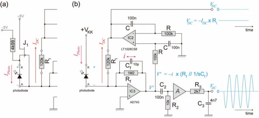
A transimpedance amplifier with a single-PD input was designed to address the requirements listed 1–5 above, and its circuit diagram is shown in Figure1(b), with a subsequent modification that was made to it shown in Figure1(a).
Circuits similar to that shown in Figure1(b)—if taken from the PD detector up to the node bearing the labelV’— have been described previously for the purposes of “rejecting ambient light,”13 or for the “control of ambient light.”14 In this work, however, the op-amp based circuit shown in the figure does not discard theDCphotocurrent, but rather uses it in order to create a separate “DC” output channel—to be employed, ultimately,
(i) for aligning the shadow onto a dual-PD sensor,
(ii) for calibrating theDC, and henceAC, responsivities to fibre- (shadow-) displacement, and
(iii) for sensing the pendulum-mode motion mentioned above—also employed in (i).
In Figure 1,IPhoto is the full (DC +AC) photocurrent generated in the PD by the illuminating source, with the fi-bre’s shadow falling over one edge of the rectangular PD. In the following discussion this current has been decomposed explicitly into its steady-state and time-varying (VM) parts, such thatIPhoto=IDC+i.
In Figure1(b)the “debout” (i.e., non-inverting) integra-tor feedback around IC3, involving IC2 and its two resisintegra-tors R, and capacitors, C, forces themean, steady-state,DC out-put of IC3 always to be close to zero volts. A zero-average input to the integrator can occur only when noDC photocur-rent flows through the resistor, Rf, and under these conditions the output of IC2, labelledVDCin the figure, must be frozen at whatever happened to be its existing—negative—value at the time the “zero volts average” condition was achieved at the output of IC3. Accordingly, the fullDCphotocurrent,IDC, must flow from the anode (A) of the PD, which is a virtual Earth point (at the inverting input to IC3), down through re-sistor Ri, and into the output of IC2, which acts as a DC
current-sink. Thus,VDC= −IDC×Ri, as indicated in the
fig-ure: theDCtransimpedance gain of the amplifier is therefore 120 k.
On the other hand, none of theAC photocurrent i can flow through resistor Ri, because the output of the sluggish integrator IC2 cannot follow this HF signal so as to produce a suitable driving voltage for it across resistor Ri—due the long RC time-constant of integration.
FIG. 1. Schematic of the single-input amplifier. (a) A subsequent modification made to the amplifier shown in (b). This involved “bootstrapping” any signal present at the (large area) photodiode’s Anode (A) to its Cathode (K), via the source-follower J1. This prevented any signal current from flowing through the capacitance of the photodiode and its connecting cable: refer to the text. Here, a small reverse bias VKK∼0.5 V appeared across the photodiode. (b) “Debout,” or non-inverting, integrator feedback via IC2 (together with the two resistors labelled R and the two capacitors labelled C), forced themeanoutput voltageV of IC3 always to be close to zero volts, causing theDCand “Violin-Mode”ACcomponents of the photocurrent,IDCandi, respectively, to follow the different paths indicated in the figure (refer to the text). The voltage gainA=101.
However, the output of transimpedance op-amp IC3 is free to respond to photocurrenti, by taking up anAC volt-age at its output given byV’= −i×[impedance of Rf //Cf]. Indeed, for frequenciesf<13.2 kHz, anyACphotocurrenti
must flow essentially through the transimpedance resistor Rf, alone. Thus, theACViolin-Mode transimpedance gain of the amplifier—to the node labelledV’—is 1.2 M.
In sum: the non-inverting integrator feedback forces the
DCand “Violin-Mode”ACphotocurrents to follow the differ-ent paths indicated in the figure.
Furthermore, in Figure1(b)theVMsignalV’isAC cou-pled by the high-pass filter C2–R2, for frequencies above
∼160 Hz, to the input of a voltage amplifier having a gain ofA=101 (for this single-PD amplifier; and A=100 for the differential amplifier), before being additionally band-limited in its response on the high-frequency side by the low-pass fil-ter R3–C3, which has a single-pole roll-off above 12.5 kHz.
The output of this filter was the final “Violin-Mode” out-put voltage of the amplifier, VAC, as indicated in Figure 1. FromV’onwards the mean value of thisACvoltage was zero, so that saturation/clipping of large signals were symmetrical.
B. The transimpedance amplifier: Reducing input capacitance
TheHamamatsuS2551 silicon photodiode15was used in both the single and differential shadow-sensors, this having an effective detection area measuring 1.2 mm ×29.1 mm. Because of its large area (∼35 mm2), this PD had a relatively large capacitance: 350 pF, at zero bias. However, as a con-sequence of an additional capacitance of 600 pF, or more, in parallel with the PD, due to a necessary coaxial cable run of
∼6 m between the photodiode(s) and the amplifier, a total input capacitance of Cin ∼1000 pF was anticipated.
There-fore, the necessarily small value of feedback capacitance Cf(=10 pF) meant that this was, unfortunately, an ideal con-figuration for “noise gain peaking”—where the input voltage noise of op-amp IC3 is effectively multiplied-up by a factor of 1+Cin/Cf(∼100, here).12
This undesirable effect was mitigated first by choosing a low-noise op-amp for IC3 (initially an AD743: 5.0 nV/√Hz, max., at 1 kHz; and later, because of its much smaller SMD footprint, an OPA627AU: 5.6 nV/√Hz, typ., at 1 kHz); and second by adding the circuitry shown in Figure 1(a), which followed a scheme described in Ref.12. The prototype am-plifier’s original input circuit, shown in Figure 1(b), there-fore was modified by the addition of the very low-noise JFET transistor, J1 (BF862:∼1 nV/√Hz), connected as a source-follower, along with its simple biasing circuitry. This tran-sistor “bootstrapped” the signal from the photodiode’s An-ode (A)—such that any signal present at this “virtual-earth” point (arising from IC3’s falling open-loop gain with ris-ing frequency) was transferred to the photodiode’s Cathode (K), so that very little signal voltage now appeared across
Cin. Consequently, a correspondingly reduced signal current now would be able to flow through the capacitance of the photodiode and its connecting cable—making them appear very much reduced in capacitance, and so greatly diminish-ing any noise gain peakdiminish-ing. The presence of transistor J1also provided a small but useful reverse bias to the photodiode (∼0.5 V), which slightly decreased its capacitance.
The addition of the transistor J1 altered neither theDC
nor theACsignal behaviour of the single-input amplifier, and so, from Figure1(b), its “DC” output signal can be expressed straightforwardly in terms of the complex frequency s [s=jω, j≡√(−1)], by a transimpedance relationship of the form,
VDC IDC = −
Rf (s2CRC
fRf+sCR+Rf/Ri)
. (1)
Clearly, for a trulyDC component of photocurrent (s= 0) Eq.(1)reduces to the simple expressionVDC = −IDCRi, as derived above. For the component values given in Figure1(b), the expression in Eq.(1)is effectively that of a low-pass re-sponse, with a dominant pole at 161 Hz (and a second, HF, pole at 13.1 kHz): therefore, 0.6 Hz “pendulum-mode” sig-nals were passed without attenuation to the amplifier’sDC
output.
In a similar fashion, theratio of the amplifier’sAC re-sponse to a VMsignal photocurrent, to its DCresponse to a steady quiescent photocurrent (a convenient ratio) can be found to be
VAC VDC(s=0)
= A(Rf/Ri)s2CRC2R2
(s2CRC
fRf+sCR+Rf/Ri)(sC2R2+1)(sC3R3+1) .
(2)
Here: A= 101, Cf =10 pF, Rf =1.2 M, Ri =120 k, C = 100 nF, R = 100 k, C2 = 100 nF, R2 = 10 k, C3 =4.7 nF, and R3 =2.7 k.Equation(2) effectively ex-presses the relative sensitivity of the amplifier’sACandDC
outputs to changes in photocurrent due tothe same displace-ment of a fibre’s shadow across (the edge of) the PD detector: in theACcase a change occurring at a frequency s (=jω) for a sinusoidal modulation at angular frequency ω; and in the
DCcase a change occurring from one steadyDCvalue to an-other, as the fibre’s shadow made a quasi-static displacement. Practically, this relationship was used to calibrate the sensi-tivity toVMdisplacement of the fibre, at any given frequency
f(=ω/2π), relative to the—straightforwardly measurable— rate of change of DC output voltage VDC with silica fibre (shadow) position. Refer to Ref.16.
In practice, the theoretical mid-band (∼1.48 kHz)AC/DC
gain ratio given by Eq.(2)did not quite peak at the anticipated value of 101 ×10=1010 but was slightly reduced by the sharply circumscribed (four poles/two zeroes) pass-band of the amplifier, as discussed below.
C. Prototype amplifier: Practical NIR gain calibration
A calibration system was built to verify that Eq.(2) prop-erly described both theAC andDCbehaviours of this am-plifier. This system involved irradiating the amplifier’s sin-gle photodiode detector with a very low intensity beam de-rived from an OD50L NIR LED, using a pin-hole aperture, the beam consisting of a steady component of fixed intensity, plus a small sinusoidal intensity modulation on top of this at a known frequency,f.17
The results of such measurements of theAC/DCgain ra-tio as a funcra-tion of the frequencyf agreed with the theoret-ical expression given by Eq.(2)at a±1% level up to∼100 kHz, i.e., well above the required VMbandwidth of 5 kHz. Consequently, as mentioned above, a bench measurement of the shadow-sensor’s quasi-static responsivity to shadow- (i.e., suspension fibre-) displacement (hereinafter called the “DC
responsivity”), allowed the correspondingACresponsivity to
be inferred with a high degree of confidence from the mea-sured AC/DCgain ratio at any given VMfrequency,f. This was the technique used to calibrate the amplifier’sAC respon-sivity as a function off.16,17 In practice the gain was found to be 1000 mid-band at 1.48 kHz and 990 at 1 kHz (and 976
±4 mid-band for the differential amplifier, described below, at 1.48 kHz).
III. THE DIFFERENTIAL VIOLIN-MODE AMPLIFIER
Following the successful performance of the prototype amplifier, connected to a single rectangular photodiode sen-sor, it was clear that a differential sensor would improve the signal-to-noise ratio by a factor of√2. Two closely adjacent
Hamamatsu S2551 photodiode elements, orientated so that the fibre’s shadow fell along their common vertical edge, and sensing differentially, could in principle double the size of the availableACphotocurrent signal, whilst offering a degree of common-mode rejection, as well.
A. The differential amplifier: From concept to construction
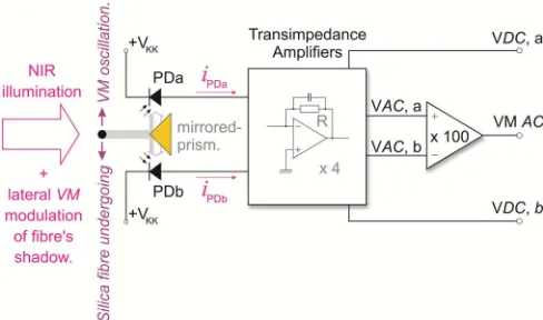
[image:4.612.316.560.514.658.2]The outline design of the Transimpedance Amplifiers block is shown in Figure 2. It is essentially a dual version of the prototype amplifier, but with an intermediate, differen-tial,ACamplification stage. For the photodiode element PDa in Figure2,Iarepresents the “DC” value of its photocurrent, inclusive of any pendulum-mode modulation, whilst ia rep-resents any HF modulation of this photocurrent due to trans-verseVMoscillation of its monitored fibre (and shadow). Sim-ilar nomenclature has been used for element PDb. Note that the modulation photocurrentsiaandibflowed automatically in anti-phase for the “synthesized split–photodiode” detec-tor: if the silica-fibre’s shadow moved over the common edge of elements PDa and PDb, so as to move off PDa (by any
FIG. 2. Schematic diagram of the Violin-Mode shadow-sensor connected to its “Transimpedance Amplifiers” block (differential amplifier), with the “syn-thesized split-photodiode-” based sensor being shown in plan view. The mir-rored prism split the collimated incident NIR illumination so that it, together with a variable fraction of the fibre’s shadow, fell onto each photodiode sen-sor element—as if the separate photodiodes formed a single split-photodiode detector, with negligible dead-band between the two elements. Here, the full photocurrents flowing in photodiode elements PDa and PDb have been des-ignated, respectively,iPDa=Ia+iaandiPDb=Ib+ib(refer to the text).
amount) and onto PDb, then the illumination of PDa, and thereby its photocurrent, iPDa, increased; but as the shadow moved off element PDa it moved automatically onto element PDb, thereby decreasingiPDbby closely the same amount by whichiPDa was increased.16 The amplifier’s two “DC” volt-age outputs, labelled VDC,a and VDC,b in the diagram, were derived from theDCphotocurrentsIaandIb, respectively, via a transimpedance gain of R=120 k. Similarly, the inter-mediateACsignal voltages VDC,a and VDC,b were derived fromiaandib, respectively, but in this case via a ten-times-larger transimpedance gain of R=1.2 M. These two tran-simpedance signals were then differenced, and their resulting differential voltage was amplified further by a factor of×100, so as to produce the final Violin-Mode output voltage VMAC. In this way, and measured from an individual photodiode element to its own respective pair of outputs, the overallAC
transimpedance gain was measured to be (976±4)×theDC
gain (mid-band), or approximately 1% lower than that of the single-input amplifier, as expected, given the slightly lower value of theACgain stage in this amplifier.
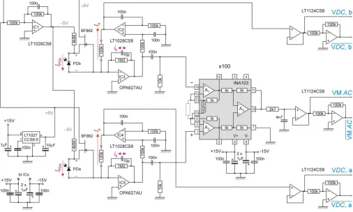
The full circuit diagram of the differential amplifier is shown in Figure3, and the realization of two such amplifiers on a pair of small Printed Circuit Boards, using surface-mount components, is shown in Figure4. It is noteworthy that an earlier version of the differential amplifier, which was built using through-hole mounted components, gave an equally good noise performance in the pass-band, but did not conform
quite so closely to the theoretical high frequency performance as did the surface-mount amplifiers—as exemplified by Figure5. Four differentialVMamplifiers and shadow-sensors were built, one per suspension fibre of a full test-mass mirror suspension.
B. The differential amplifier: Signal and noise performance
A typical noise Power Spectral Density (PSD) of the dif-ferential amplifier, measured at its VMACoutput, is shown in Figure 5. The −3 dB bandwidth was found from a fit of Eq. (2) to these noise data to lie between 226 Hz and 8.93 kHz. The theoretical pass-band is indicated by the la-belled solid (blue) line in the figure and it is seen to be a very good fit to the measured noise PSD for frequencies above
[image:5.612.53.559.396.700.2]∼50 Hz. Moreover, the peak, mid-band, noise PSD was found to lie very close indeed to the fundamental shot-noise limit, as indicated in the figure by the horizontal (red) line. Here, this limit was calculated from the two measuredDCphotocurrent values by assuming that the shot noise arising from the two photodiode elements was uncorrelated. The roll-off of the am-plifier’s gain towards both lower and higher frequencies was at a rate of−40 dB/decade. Given the measured mid-band noise PSD of−63.2 dBV(rms)/√Hz (≡692μV(rms)/√Hz), the broad-band rms noise voltage was expected to be 68 mV
FIG. 3. Circuit diagram of the Violin-Mode differential shadow-sensing transimpedance amplifier sensor (with photodiode sensing elements PDa and PDb). Three complementary outputs were made available for driving long cables, if necessary (refer to the text). This also allowed positive versions of the twoDC outputs, VDC,a and VDC,b, to be used. The INA103 instrumentation amplifier is a 1 nV/√Hz device. Four such amplifiers were constructed—one per silica fibre. Two of these amplifiers are shown, as constructed, in Figure4. For coaxial output cables>2.5 m in length, 600resistors were added directly in series with the six outputs, to prevent oscillation.
FIG. 4. Two of the four SMD-based amplifiers were constructed on the pair of PCBs shown in the figure, each amplifier being of the type shown in Figure3. The PCBs measured 60 mm×60 mm, such that they could be stacked one above the other within a compact square enclosure. Each amplifier was interfaced to a particular (differential photodiode based) shadow-sensor, a separate sensor being dedicated to each one of the four suspension fibres of a full test-mass/mirror suspension.
(rms)—very close to the measured value, as seen in Figure6. Note that the split supply rails for the amplifiers both bene-fited from “noise finessing” filters, in order to reduce voltage regulator noise.18
An actual VM signal resulting from an approximately 1μm peak-peak acoustically induced fibre resonance, at a fre-quency of 1019.1 Hz, is also shown in Figure6. Here, a sin-gle capture of theVM ACsignal is seen to be approximately 10 V, peak-peak. Twenty three volts peak-peak (approx.
2.4μm, peak-peak) signals could have been accommodated, without clipping or distortion.
C. The differential amplifier: DC and AC responsivities
In practice, quasi-DCpendulum-mode signals were de-tected using theDCoutputs of these amplifiers, and signals with amplitudes of up to±140μm, peak-peak, at 0.64 Hz, were detected.9 These sameDC outputs were used also for
FIG. 5. Noise Power Spectral Density of the differential amplifier as a function of frequency, measured at theVM ACoutput of the amplifier. The fundamental mid-band shot noise limit is marked by the horizontal line in the figure, at−63.2 dBVrms/√Hz. The theoretical amplifier Passband, as described by Eq.(2), is indicated by the blue line. Here, the fibre’s shadow fell over neither detector element, in order to avoidVMand other resonant peaks, and so the noise PSD is higher in this figure at 500 Hz, say, than when the shadow fell over the adjacent edge of both detector elements—as it must for properVMdetection. The reduction in noise PSD with the shadow present was approximately 0.8 dB, in fact. The noise reduction was due entirely to the lower levels ofDCphotocurrent, and so shot noise, in the two partially shaded PD elements.7
[image:6.612.130.486.427.687.2]FIG. 6. (Left) The differential amplifier’sVM ACoutput, showing an acoustic excitation of the fundamental Violin-Mode of a 95 mm long silica fibre sample, 0.4 mm in diameter, using a distant loudspeaker. A single capture of the resulting Violin-Mode waveform is shown, at approximately 10 V, peak-peak, and so the amplitude of the test fibre’s transverse Violin-Mode motion was approximately 1μm, peak-peak. The resonant frequency was found to be 1.0191 kHz. (Right) Photo of the Tektronix TDS-3052B oscilloscope screen, showing the amplifier’s typical broadband output noise level to be∼68 mV (rms) at the amplifier’s VM ACoutput—in agreement with theory for this wide frequency band. The horizontal bars have been set approximately at the±2σlevels.
displacement calibration, and in bench tests theDC respon-sivity of each photodiode detector+amplifier was measured by translating laterally a test fibre, mounted vertically on a motorised stage, through the NIR beam of each shadow sen-sor. In this way, the DC responsivity was found.16 Taken
over the four detectors and their respective amplifiers, it was measured to be 10.44 kV m−1 of fibre displacement. From
this value, the AC responsivity was deduced to be (9.43
±1.20) MV(rms) m−1(rms), when taken over the four de-tectors/amplifiers, since theAC/DCgain ratio was measured to be 904 at this frequency.
With an exceptionally lowVM ACoutput noise PSD at 500 Hz of (−64.0 ±0.5) dBV(rms)/√Hz, when taken over all four—partially shaded—detectors, and with the highAC
responsivity of the detection system given above, the limiting displacement sensitivity of the full shadow sensor/amplifier system was found to be (69±13) picometres (rms)/√Hz at 500 Hz, over a measuring span of ±0.1 mm—thus exceed-ing its target sensitivity of 100 picometres (rms)/√Hz, at this frequency, and over this measuring range.7–9
IV. CONCLUSIONS
The noise level measured for the differential amplifier was little different from the fundamental limit expected from (uncorrelated) shot noise in its two photodiode detector ele-ments. Indeed, the “white noise” region of the differential am-plifier’s Power Spectral Density followed its theoretical pass-band very closely over the frequency range investigated, as seen in Figure5, only deviating above this form for frequen-cies below∼50 Hz, where 1/f noise began to dominate. Both versions of the amplifier exhibited close-to the theoretically expected signal gain, with the AC/DCgain ratio mid-band (1.48 kHz) being very close to the expected value of approx-imately 1000. Moreover, the signal gain at the
“pendulum-mode” frequency of ∼0.6 Hz was, by a very useful factor of >70 000 (97 dB), smaller than that found mid-band— allowing Violin-Mode signals in the range 500 Hz–5 kHz to be detected, even in the presence of very much larger pen-dulum motion of the test mass and its supporting fibres. The differential amplifier’sACpass-band extended from 226 Hz to 8.93 kHz (−3 dB), and its very low noise level allowed it, in principle, to recover a 500 Hz sinusoidal Violin-Mode vibration of amplitude (69 ±13) picometres (rms), in one second. Yet, this amplifier output could handle, without clip-ping or distortion, a similar signal of amplitude 2.4 μm (or
∼23 V), peak-peak. The subsidiary “DC” outputs had a de-signed (DC) responsivity to quasi-static shadow displacement that was lower than the mid-bandACresponsivity by a factor of approximately 1000. These outputs therefore exhibited a much larger detection range for shadow displacement, with a bandwidth extending from trueDC– 160 Hz (−3 dB point). This allowed pendulum-mode signals at 0.64 Hz, and of am-plitude exceeding 200μm peak-peak, to be captured without attenuation. In summary, the differential Violin-Mode ampli-fier described above clearly met, or exceeded, all of its perfor-mance targets.
At the time of writing the Violin-Mode sensor system mentioned here has not been adopted for aLIGO, and, in-deed, the need for VM damping has not yet been demon-strated. However, if it is found to be required, the current baseline solution is to use aLIGO’s Arm Length Stabilisation system as aVMsensor.19 In fact, the issue of vacuum com-patibility remains unresolved for the VMsensor mentioned here, because theHamamatsu photodiodes used for the de-tector elements had been encapsulated, using an unknown epoxy. However, were it to become necessary, the issue of the epoxy for the photodiodes from this, or another, manufacturer probably could be resolved, and the LEDs and other com-ponents used are likely to prove vacuum compliant, or have
[image:7.612.60.560.53.250.2]vacuum-compliant alternatives. Nevertheless, theVM ampli-fier described here may find other applications.
ACKNOWLEDGMENTS
We thank the IGR, University of Glasgow, Scotland, UK, for the silica fibre test samples used in this work, and ac-knowledge that without the research of Alan Cumming, Giles Hammond and Liam Cunningham of that institution on de-velopment and construction of the prototype aLIGO test-suspension used in obtaining the Violin-Mode results reported here, the work reported in this paper would not have been pos-sible. We also thank Angus Bell of the IGR, Norna Robertson and Calum Torrie of Caltech and the IGR, Dennis Coyne of Caltech, Peter Fritschel, David Shoemaker, Rich Mittleman, and Brett Shapiro of MIT, Ludovico Carbone and Alberto Vecchio of the University of Birmingham, and Justin Green-halgh of the CCLRC (RAL), for their oversight of, and assis-tance with, this work. We are grateful to John Broadfoot, Ged Drinkwater, Ken Gibson, and Mark Hutcheon, of the Physics Department’s Electronics Workshop, and to the staff of the Science Faculty’s Mechanical Workshop, at the University of Strathclyde, for their careful construction of most of the com-ponent parts used in this work. Finally, we are grateful for the support of grant STFC PP/F00110X/1, which sustained this work.
1G. M. Harry (for the LIGO Scientific Collaboration), “Advanced LIGO:
the next generation of gravitational wave detectors,”Classical Quantum Gravity27, 084006 (2010).
2B. P. Abbottet al., “LIGO: The laser interferometer gravitational-wave
ob-servatory,”Rep. Prog. Phys.72, 076901 (2009).
3F. J. Raab, “Overview of LIGO instrumentation,”Proc. SPIE5500, 11–24
(2004).
4S. M. Astonet al., “Update on quadruple suspension design for Advanced
LIGO,”Classical Quantum Gravity29, 235004 (2012). 5A. Heptonstallet al., “Invited Article: CO
2laser production of fused silica fibres for use in interferometric gravitational wave detector mirror suspen-sions,”Rev. Sci. Instrum.82, 011301-1–011301-9 (2011).
6A. V. Cumming et al., “Design and development of the advanced
LIGO monolithic fused silica suspension,”Classical Quantum Gravity29, 035003 (2012).
7N. A. Lockerbie, K. V. Tokmakov, and K. A. Strain, “A source of
illumi-nation for low-noise ‘Violin Mode’ shadow sensors, intended for use in interferometric gravitational wave detectors,”Meas. Sci. Technol.(to be published).
8N. A. Lockerbie and K. V. A. Tokmakov, “Violin-Mode’ shadow sensor
for interferometric gravitational wave detectors,”Meas. Sci. Technol.(to be published).
9N. A. Lockerbie, L. Carbone, B. Shapiro, K. V. Tokmakov, A. Bell, and K.
A. Strain “First results from the ‘Violin-Mode’ tests on an advanced LIGO suspension at MIT,”Classical Quantum Gravity28, 245001 (2011). 10L. Carboneet al., “Sensors and actuators for the Advanced LIGO mirror
suspensions,”Classical Quantum Gravity29(11), 115005 (2012). 11A. V. Dmitriev, S. D. Mescheriakov,K. V. Tokmakov, and V. P. Mitrofanov,
“Controllable damping of high-Q violin modes in fused silica suspension fibers,”Classical Quantum Gravity27, 025009 (2010).
12G. Brisebois, Linear Technology Design Note DN399: Low Noise
Amplifiers for Small and Large Area Photodiodes, 2008, see http://cds.linear.com/docs/Design%20Note/dn399f.pdf.
13M. Stitt and W. Meinel, “OPT201 Photodiode-Amplifier Rejects Ambient
Light,”Burr-Brown IC Applications Handbook(1993), p. 379.
14M. Johnson, Photodetection and Measurement (McGraw-Hill, 2003),
p. 146.
15Seehttp://www.hamamatsu.com/for Hamamatsu S2551 photodiodes. 16N. A. Lockerbie and K. V. Tokmakov, “Quasi-static displacement
calibra-tion system for a ‘Violin-Mode’ shadow-sensor intended for gravitacalibra-tional wave detector suspensions,”Rev. Sci. Instrum.85, 105003 (2014). 17N. A. Lockerbie and K. V. Tokmakov, A modulated Near InfraRed gain
calibration system for a ‘Violin-Mode’ transimpedance amplifier, intended for advanced LIGO suspensions (TBA) LIGO-G1401275-v1, available at https://dcc.ligo.org.
18See http://www.wenzel.com/documents/finesse.htmlfor Finesse Voltage
Regulator Noise! (Wenzel Associates Inc.).
19Instrument Science White Paper LIGO-T1200199-v2, p71, 2012, see
https://dcc.ligo.org.