Abstract—The three-phase two-level voltage source converter (VSC) is widely employed in power conversions between AC and DC for its four-quadrant operation and control flexibility. However, it suffers from the low output voltage range with a peak value of half DC-link per phase, which necessitates the use of either high DC-link voltage or bulky step-up transformer to enable the medium voltage operation. Additionally, the high common mode (CM) voltage between AC loads neutral points and ground may reduce the service life and reliability of electric machinery. In this paper, a three-phase AC side voltage-doubling VSC topology with intrinsic Buck-Boost cell is analyzed. By this configuration, the AC side voltage is doubled with the phase peak value equal to DC-link. That is, only half of the DC side capacitor bank is needed to generate the same output voltage. The proposed converter uses its buck-boost cell as a virtual voltage source to synthesize negative half of the output voltage by modulating its output AC phase voltage around the negative bus (which is the real zero when grounded). This permits the average CM voltage to be suppressed to zero, and loads connected to converter AC side not to withstand any DC voltage stress (reducing the insulation requirement). Modeling and control design for both rectifier and inverter modes of this converter in synchronous reference frame have been investigated to ensure a four-quadrant three-phase back-to-back system. Experimental results have verified the feasibility and the effectiveness of the proposed configuration and the designed control strategies.
Index Terms— AC side voltage-doubling, Common mode voltage suppression, Intrinsic Buck-Boost Cell, Three-phase Back-to-Back system, Four-quadrant operation.
I. INTRODUCTION
ower electronics based energy conversion systems have achieved deep penetration in low, medium and high voltage applications such as power transmission and reactive power compensation, grid interfacing of renewable energy, machine drives, etc. Since traditional AC grids still dominate in power systems, AC power conversion involving
Manuscript received on August 1, 2014; revised on September 23, 2014; accepted on October 24, 2014. This work was supported by EPSRC ‘Underpinning Power Electronics 2012: Converters Theme’ research programme (EP/K035096/1).
P. Li, G.P. Adam, Y. Hu, D. Holliday, B. Williams are with Department of Electronics and Electrical Engineering, University of Strathclyde, Glasgow, G1 1XW, UK. (e-mail: [email protected], [email protected], [email protected], [email protected], barry.williams@ eee.strath.ac.uk).
amplitude regulation, phase and frequency control, active power and reactive power management for utility/micro-grid applications has always drawn many attentions of both academia and industry.
The back-to-back (B2B) VSC configuration is widely used among various AC conversion solutions for its superiority on control simplicity, voltage utilization over the Matrix Converter and dynamic performance over other current source converter based solutions [1, 2]. This is because it offers four-quadrant operation ability, decoupling of the two connected AC sides and independent control of active/reactive power. Nowadays, VSC together with its B2B configuration have overstepped the traditional power traction area and spread into the utility applications, such as PV (photovoltaic) grid connection, wind energy interfacing, flexible AC and high voltage DC transmission systems (FACTS and HVDC) [3-9].
Fig. 1 Three-phase two-level voltage source converter.
The three-phase two-level converter depicted in Fig. 1 is widely accepted for AC-DC and DC-AC power conversion systems in research and industry. However, in this topology, the peak value of AC side voltage per phase cannot exceed half of DC link voltage with traditional Sinusoidal Pulse Width Modulation (SPWM). Although the Triplen Sinusoidal Pulse Width Modulation (TSPWM), Space Vector Modulation (SVM) and Selective Harmonic Elimination (SHE) methods have been developed to extend the fundamental voltage output range in AC side, the increase is not obvious (15.5% for TSPWM/SVM, and slightly larger for optimized SHE) [10]. In addition, three-phase balanced conditions should be guaranteed to insure this extension in voltage utilization, otherwise, low order harmonics will be observed in the line-to-line voltages and line currents. This is because zero sequence components will emerge in phase voltage when it goes beyond the envelopes of the positive and negative DC-link, which can only be neutralized under three-phase balanced situation. Therefore, operation in medium and high voltage applications requires high DC-link voltage (minimum of twice peak fundamental voltage) or the bulky step-up
Three-Phase AC Side Voltage-Doubling High
Power Density Voltage Source Converter with
Intrinsic Buck-Boost Cell and Common Mode
Voltage Suppression
Peng Li, Grain Philip Adam
Member IEEE
, Yihua Hu
Member IEEE
, Derrick Holliday and Barry Williams
transformer for voltage matching, which in turn increases the system cost, size and weight.
The CM voltage between AC and DC sides is inherent for all bridge type solutions. The three-phase two-level VSC in
Fig. 1 may impose DC voltage stress on the AC side loads depending on the adopted grounding arrangement [11, 12]. When the negative terminal is grounded, the output phase voltage relative to real ground varies around half DC-link, and this requires the AC loads to be able to withstand DC voltage stress [13]. Furthermore, the voltage fluctuation around half DC-link on the load neutral point may exacerbate the bearing voltage problem in machine drives such as wind turbine interfacing. The split DC-link capacitor with parallel balancing resistors can be employed to address the problem of DC voltage stress and reduce the impact of the CM voltage. However, this solution is less attractive as it introduces additional loss and cost.
A certain case under the spotlight recently is the transformerless PV integration area where many efforts have been made to diminish this CM component across the parasitic capacitor between the PV arrays and ground. The H5, H6 and HERIC schemes are candidates to suppress the CM leakage current [14]. However, the CM voltage component still exists and keeps constant in these situations. The virtual DC bus concept [15] and HA4S converter [16] have been advanced to eliminate the CM voltage by direct connection between ground terminals. Unfortunately, the solutions above are in single-phase application and originate from the H-bridge topology. Thus, it is difficult to transplant these derived converters directly into three-phase condition.
In this paper, a three-phase AC side voltage-doubling (ACVD) converter with intrinsic Buck-Boost cells (IBBCs) has been proposed, which can generate the AC phase voltage with a maximum peak value equal to full DC-link voltage, doubling the output range of the traditional three-phase two-level VSC. On the other hand, the DC-link can be halved when the same output voltage is demanded. Consequently, either the line transformers or the DC capacitor bank can be reduced to form a compact and cost-efficient system. In addition, the dv/dt problem can be largely relieved by the reduced DC-link voltage. Since the proposed topology inherits a real ground fixed at negative bus, its output phase voltage is modulated around this ground. As a result, DC voltage stress exerted on the AC loads can be suppressed to zero, and this will suppress the magnitude of CM voltage to an average of zero, as seen by the load neutral points. Hence, reduced bearing voltage/current can be expected. Further employment of either composited hardware configuration or optimized modulation strategy can eliminate the high frequency components of the CM voltage, which is beyond the scope of this paper [17-19]. The ACVD converter is capable of being employed in PV integration, wind energy interfacing and distributed FACTS areas potentially. The rest of the paper is organized as follows. Operational principle of the proposed converter is described in Section II. Section III analyses the voltage and current stresses on the power switches and presents some design issues for passive components. In Section IV, modeling process of the three-phase ACVD-VSC for inverter and rectifier modes in synchronous reference frame (SRF) is established. Then, Section V presents the
design of the control strategies minutely. Afterwards, experimental verifications are presented in Section VI to confirm the validity of the proposed converter. Finally, conclusions drawn and highlight of major findings are summarised in Section VII.
II. OPERATIONAL PRINCIPLE OF THE ACVDCONVERTER
The proposed three-phase ACVD-VSC is shown in Fig. 2(a), where the IBBC is inserted into each phase of two-level converter to achieve an extended output voltage range. The single-phase circuit under inverter mode depicted in Fig. 2(b)
clarifies the structure of the topology in detail. It can be seen that the IBBC consists of L1 and C1, while L2 and C2 make up
the output stage filter. The two power switches S1 and S2
conduct complementarily. Furthermore, Vdc is the input
voltage, and i1, v1, i2 and v2 represent the four state variables
on the passive components L1, C1, L2 and C2 respectively.
Notice that v1 should be reversed relative to the input voltage
to ensure the magnetic reset of the flux linked in L1. Similarly,
i1 and i2 are also in opposite directions to keep the voltage
balance on C1.
(a) (b)
Fig. 2 Proposed ACVD Converter: (a) configuration in three-phase (without filter); (b) single-phase unit operated in inverter mode.
Operation of the proposed converter can be described using two modes as follow:
Mode 1: S1 is turned on. Output voltage v2 fed from Vdc is
generated relative to ground. Also, this mode creates a zero loop of inductor L1 and capacitor C1 for charging the
buck-boost capacitor with reversed polarity as Vdc.
Mode 2: When S2 is on, the IBBC capacitor is employed as
a virtual voltage source to generate the negative voltage on the output. The inner inductor L1 is also charged to store energy to
[image:2.612.313.560.296.408.2]get ready for the energy transfer in the subsequent switching cycle.
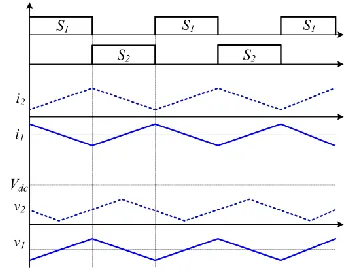
Fig. 3 Steady state waveforms of the proposed converter in a stationary operation point when v2, i2 are positive and i1 is negative
[image:2.612.347.519.557.694.2]assumption that v2, i2are positive andi1is negative. The output
voltage v2 always falls inside the envelope combined by input
voltage and IBBC voltage, which guarantees the energy balance in the inductance. Similarly, the inductor currents i1
and i2 will charge and discharge the capacitors in each
switching cycle to obtain the composed voltage outputs. In further, the four-quadrant operation of the ACVD-VSC is interpreted by Fig. 4. In Fig. 4(a) and Fig. 4(b), i2 flows out
of the converter to the load, accordingly i1 should either
discharge C1 or feed its stored energy back to the DC-link.
The alternative situation where i2 flows into the converter
from the load and i1 draws energy from the DC side to deliver
it to C1 can be seen in Fig. 4(c) and Fig. 4(d). Thus, it is
concluded that the proposed converter is a qualified candidate for the four-quadrant operational VSC applications.
(a) (b)
[image:3.612.343.523.219.589.2](c) (d)
Fig. 4 Switching modes for the proposed converter to implement four-quadrant operation: (a) S1 turns on with outflow load current; (b) S2
turns on with outflow load current, (c) S1 turns on with inflow load
current, (d) S2 turns on with inflow load current.
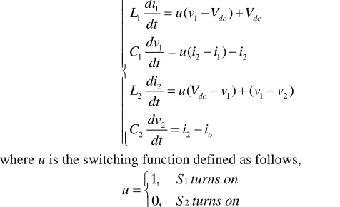
Based on the above analysis, the differential equations that describe the dynamics of the proposed converter are interpreted in (1),
1
1 1
1
1 2 1 2
2
2 1 1 2
2
2 2
( )
( )
( ) ( )
dc dc
dc
o
di
L u v V V
dt dv
C u i i i
dt di
L u V v v v
dt dv
C i i
dt
(1)
where u is the switching function defined as follows,
1
2
1, 0,
S turns on u
S turns on
(2)
Considering the case where switching frequency is sufficiently high compared to fundamental frequency of the AC voltage being synthesized, the assumption that all the state variables can be viewed as constant is valid. Therefore, the derivative terms in (1) can be set to zero, and the average
value of the switching function u over one switching period is equal to the duty cycle D, then equation (1) is reduced to:
1
2 1 2
1 1 2
2
( ) 0
( ) 0
( ) ( ) 0
0
dc dc
dc
o
D V V V
D I I I
D V V V V
I I
(3)
After algebraic manipulation of first and third equations in
(3), voltage transfer ratio of proposed converter is obtained as:
2 1
2
dc
V M
V D
(4) Fig. 5(a) shows the plot of M versus D and it is observed that a bipolar voltage output can be achieved when the duty cycle varies around 0.5.
(a)
(b)
(c)
Fig. 5 Voltage output range and modulation for the proposed converter: (a). voltage transfer ratio vs. duty cycle; (b). AC side output voltage range; (c). open loop modulation strategy based on transfer ratio.
From Fig. 5(b), the maximum modulation index is 1pu for the peak value of phase voltage (Vdc), which is twice of that in
two-level converter (½Vdc). In addition, triplen harmonic
injection idea can further extend this range to 1.55pu. Equivalently, the output line-to-line peak voltage can reach 2pu (2Vdc) in that case. Due to this large extension in DC
utilization, reduced DC-link voltage and dv/dt can be achieved. Notice that inner capacitance can be significantly less than DC link because of the fluctuant voltage across it. Besides, the asymmetry between the two voltage levels synthesized during
0
VAC
VDC
-VDC
[image:3.612.66.270.221.443.2] [image:3.612.47.285.530.675.2]modes 1 and 2 may potentially distort the output voltage by even order harmonics when the modulation strategy in Fig. 5(c)
is adopted, where Am is the modulation index. Therefore,
proper converter operation with sinusoidal output voltage and current requires countermeasures to be incorporated in the modulation strategy to neutralize the negative impact of the distortion, which will be investigated in later sections.
From the above analysis based on single-phase situation, it can be found that the DC-link and AC side share the common ground. Consequently, in the three-phase three-wire system, the average value of the CM voltage between DC-link ground and AC neutral point must be zero for any balanced condition.
III. PERFORMANCE EVALUATION OF VOLTAGE/CURRENT
STRESS AND INTEGRATED MAGNETIC SOLUTION
In this section, a brief analysis of the voltage/current stress of power switches and some design issues for the passive components are demonstrated. The additional IBBC may exert some extra voltage/current stress on the devices. So it is important to unveil the quantitative relationship between the electrical stresses of the semiconductor switches and the output power, based on which the guidelines of the device selection is provided. Besides, the integrated magnetic technique can be employed to integrate the two inductors into one magnetic core, compacting the installations and reducing the core costs.
A. Voltage Stress Analysis
According to (3), the voltage on C1 and C2 are given by (5)
and (6) respectively. The opposite polarity of Vdc and V1 offers
the possibility to generate the bipolar voltage on C2.
1 (1 1/ ) dc
V D V
(5)
2 (2 1/ ) dc
V D V
(6)
Consequently, the reverse blocked voltage of the power switches S1 and S2 can be calculated by (7).
VRB Vdc V1 Vdc/D (7)
In further, since the maximum output-input voltage ratio is Am, the voltage stress is then shown by (8).
(2 ) (2 msin )
RB dc dc
V M V A t V
(8)
It is noticed that the duty cycle D varies from 0.33-1.0 in the maximum output condition when Am reaches the peak
value 1. The maximum voltage stress on the power switches of the proposed converter is two times of DC voltage plus peak of the output phase voltage. Compared with the two-level topology, voltage stress will increase by 50% in extreme conditions. However, this increase in voltage stress is logical, because the presented ACVD converter holds the same DC utilization as full-bridge converter but with half number of switches. In other words, it has same number of switches as two-level topology but with twice DC link voltage utilization. This attribute is achieved by the incorporation of IBBC. The fluctuant voltage across C1 makes small value AC capacitor
available but causes the increase in power switches [20]. B. Current Stress Analysis
After manipulation of equation (3) for the current state variables, equations (9) and (10) are obtained, and observe that
currents i1 and i2 are in opposite direction, which is necessary
for the energy balance of the C1.
1 (1 1/ ) 2
I D I
(9)
2 2/ o
I V RI
(10)
The current of the IBBC inductor i1 should passes through
either S1 or S2 to store and release energy alternatively. From
Fig. 4, the total current for the power switches should be the sum of absolute value of the two current state variables. Since I1 and I2 are always in opposite directions, the total current
stress of each power switch can be expressed as in (11).
1 2 1 2
c
I I I I I
(11)
In general, the power switch current can be in further clarified as (12), where φ is the power factor angle, ω is the angular frequency of the output voltage and Iom represents the
maximum value of the load current.
Ic I1I2 (Iom/D) sin( t ) (12)
Considering (4), the equation (12) then can be developed as follows:
(2 sin ) sin( )
c m om
I A t I t (13)
It can be deduced that some second order harmonic current will be introduced by the IBBC. The peak value of the power switch current happens when equation (13) reaches the maximum. An approximate margin of three times of the load current should be considered in practical design. Notice that the output current of this converter is to be approximately half of that in two-level topology with the same DC-link and same power rating since output voltage can be doubled due to the introduced IBBC, which makes the current stress not to be a problem for the proposed converter.
C. Passive Device Selection
[image:4.612.347.527.420.477.2](a) (b)
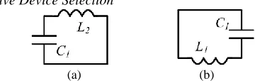
Fig. 6. Equivalent model of the power path for inner capacitor C1 of
ACVD converter: (a) S2 is on, S1 is off; (b) S1 is on, S2 is off.
Since L2 and C2 form the output filter of the proposed
ACVD converter, L2 and C2 can be selected using well
established filter design method of the conventional two-level VSC as illustrated in [21]. Whilst L1 and C1 are selected based
on the switching model from AC point of view since all the state variables are AC. The equivalent power paths for inner capacitor C1 is shown in Fig. 6. When S2 is on and S1 is off,
inner capacitor C1 is in series with output filter inductor L2 as
in Fig. 6(a). In order to make the AC component of the voltage across C1 follow up the output voltage and avoid the large
high frequency oscillation on C1, the resonant frequency of C1
and L2 is placed in the interval of fundamental and switching
frequencies (f0 and fsw). With L2, C2 and fsw are all known; the
geometrical mean in (14) is used to calculate C1 as:
1 2 0
1/ (2 )
r sw
f C L f f
(14)
In the proposed ACVD converter, the inner inductor L1 is
employed as a buffer for energy transfer from DC-link to C1 in
which can limit the inrush current from the capacitor C1 when the upper switch of each phase leg is on [22]. In Fig. 6(b), L1
and C1 are in series. Large L1 value will cause large
fundamental voltage drop and limit the magnitude of high frequency current ripple. In this sense, the characteristic impedance of L1 and C1 in (15) should be used as a
compromise between the output power range and ripple current demand.
0 1/ 1
[image:5.612.44.298.146.258.2]z L C
(15) D. Potential Use of Magnetic Integration
Fig. 7 Principles of the integrated magnetic solution.
The IBBC introduces an extra inductor into the proposed converter per phase. In order to improve the power density, the magnetic integration technique is competent to integrate the IBBC inductor and output filtering inductor into one magnetic core [23-25]. Fig. 7 interprets the solution for the magnetic integration technique, where a three-leg EE type magnetic core is employed. Some air gaps are inserted into the two outer legs while no air gap exists in the center leg. The IBBC inductor L1 is wound around one outer leg and the
filtering inductor L2 is reversely wound around another outer
leg. In this way, the magneto-motive force will be distributed mostly on the outer legs and the two inductors can be decoupled effectively. Fig. 7 shows that the flux linkage of the two inductors will be in opposite directions, so the average component of the total flux in the center leg is diminished and the cross section area of the center leg is reduced. Therefore, the power density and the efficiency can be enhanced with the proposed magnetic integration method.
This approach is restricted to low and medium power stages at present due to the limited window area of the commercial high magneto-conductivity core.
IV. MODELING OF THREE-PHASE ACVDCONVERTER IN
SYNCHRONOUS REFERENCE FRAME
The Park transformation based decoupling model for the three-phase two-level VSC is widely employed to implement independent control of active and reactive power. Since the reference becomes DC value in SRF, zero steady state errors are expected with proportional-integral (PI) controller. In this section, the modeling of the proposed ACVD-VSC in SRF is performed to establish an insight view of the control design. In order to establish a general law for the operational analysis and control design, resistive load conditions have been assumed here and in the upcoming control design section. For proper design, the load current can be treated as a new state variable. Thus, the order of the state space equations and transfer functions that describe the proposed converter will increase. Besides, extra measurements are necessary. However, the overall procedure stays the same.
The proposed converter is capable of forming a three-phase four-wire system, where the DC ground and AC ground is connected directly. Thus, each phase can be controlled independently. This configuration can be employed in UPS and aero-space applications. However, the analysis below is only based on three-phase three-wire system.
A. The Inverter Mode
Fig. 8 Rearrangement for the proposed three-phase inverter.
The rearrangement of the three-phase ACVD-VSC as an inverter is depicted in Fig. 8. From the instantaneous value based state space equations in (1) and assumptions in (16), the three-phase AC side equations can be expressed as in (17).
2 2
2
2 2 2 2
2 2 2 2
2 a b c
a b c
a b c
a b c
L L L L
C C C C
R R R R
r r r r
(16)
2 2 2 2 2 2
2 2 2 2 2 2 2 2
2 2 2 2 2 2
2 2 2 2
2 2 2 2 2
2 2 2 2
a b a b a b a b
b c b c b c b c
c a c a c a c a
a b a b
b c b c
c a c a
i i v v i i v v
d
L i i v v r i i v v
dt
i i v v i i v v
v v i i v
d
RC v v R i i
dt
v v i i
2 2
2 2
2 2
2 2 2
2 2 2 2 2
2 2 2
2 2 2
2 2 2 2
2 2
a b
b c
c a
ab ab ab ab
bc bc bc bc
ca ca ca ca
ab ab ab
bc bc bc
ca ca c
v
v v
v v
i v i v
d
L i v r i v
dt
i v i v
v i v
d
RC v R i v
dt
v i v
a2
(17)
where {va, vb, vc} represents the converter output phase
voltage (measuring from poles O={O1,O2,O3} relative to the
ground), and Vdc is the DC side input voltage. Additionally, R
and r2 are the load and filter reactor (L2) resistances
respectively.
[image:5.612.328.564.309.561.2]1 2 1, ( , , ) 0, i i i
S turns on
u i a b c
S turns on
(18)
1 1 1
1 0 0
0 1 0
0 0 1
a a a a
b b dc b b
c
c c c
v u u v
v u V u v
u
v u v
(19)
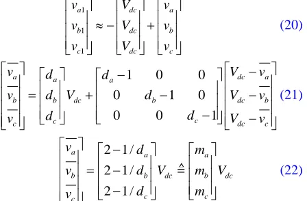
To synthesize sinusoidal output voltage based (5), the IBBC voltage is expected to contain both DC and AC components. According to the previous analysis shown by
(13), second order harmonic current will emerge in the IBBC inductor. Consequently, AC voltage of IBBC capacitor contains both the fundamental and the second order harmonic. When neglecting the second order harmonic for simplicity, (20)
is obtained. After application of the classical average method to switching function, equation (19) is rearranged into (21), which can be simplified as (22),
1 1 1
a dc a
b dc b
c dc c
v V v
v V v
v V v
(20)
1 0 0
0 1 0
0 0 1
a a a dc a
b b dc b dc b
c c
c dc c
v d d V v
v d V d V v
d d
v V v
(21)
2 1 / 2 1 / 2 1 /
a a a
b b dc b dc
c c
c
v d m
v d V m V
d m v
(22)
where {da, db, dc} is the duty ratio for each phase, {ma, mb, mc}
is the equivalent transfer ratio and “—“ is the averaging operator over one switching cycle.
Furthermore, by defining {mab, mbc, mca}={ma-mb, mb-mc,
mc-ma}, the switching averaged AC side equations can be
derived as in (23). The Park transformation with the form in
(24) is then applied to obtain the equivalent time-invariant system. The decoupling model of the proposed ACVD inverter in SRF can be finally achieved and demonstrated in (25).
2 2 2
2 2 2 2 2
2 2 2
2 2 2
2 2 2 2
2 2 2
1
ab ab ab ab
bc bc dc bc bc
ca
ca ca ca
ab ab ab
bc bc bc
ca ca ca
i m i v
d
L i m V r i v
dt
m
i i v
v i v
d
C v i v
dt R
v i v
(23)
cos cos( 2 / 3) cos( 2 / 3)
2
sin sin( 2 / 3) sin( 2 / 3)
3
1 / 2 1 / 2 1 / 2
t t t
T t t t
(24)
2 2 2 2 2
2 2 2
2 2 2 2
2 2 2 2
2 2
2 2 2 2
0 1 0 0 1 1 0
d d d d dc d
q
q q q q
d d d d
q q q q
i v i r i V m
d
m
dt i L v i L i L
v i v v
d
dt v C i v RC v
(25)
[image:6.612.78.302.246.393.2]The previous stated second order harmonic distortion problem caused by the IBBC must be treated separately with additional control loops to ensure the pure sinusoidal output voltage and current, which will be covered in later part. B. The Rectifier Mode
Fig. 9 Rearrangement for the proposed three-phase rectifier.
Fig. 9 shows the proposed ACVD-VSC when it is configured as a rectifier. The AC side and DC side equations are shown in (26), in which {vgab, vgbc, vgca}={vga-vgb, vgb-vgc,
vgc-vga} represents the AC input voltage, vdc is the output
voltage, and icon in (27) is the total current feeding from the
converter to the DC side.
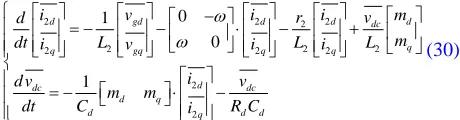
Based on the previous approximation, the second order current component in IBBC inductor is neglected temporarily. From (9) and by utilizing the switching average operator, equation (27) is to be developed into (28). After substituting
(22) and (28) into (26), the standard form of the proposed rectifier model is given as in (29).
2 2
2 2 2 2
2 2
gab
ab ab ab
bc bc bc gbc
ca ca ca gca
dc dc
d con
d
v
i v i
d
L i v r i v
dt
i v i v
dv v C i dt R
(26)
2 1 2 1 2 11 1 1
a a
b b
con a b c a b c
c c
i i
i u u u i u u u i
i i (27)
22
222 2
a ab
con a b c b ab bc ca bc
c ca
i i
i m m m i m m m i
i i (28)
2 22 2 2 2
2 2
2 2 2
gab
ab ab ab
bc bc dc bc gbc
ca
ca ca gca
ab
dc dc
d ab bc ca bc
d
ca
v
i m i
d
L i m v r i v
dt
m
i i v
i
d v v
C m m m i
dt R i (29)
2 2 2 2
2 2 2
2 2 2
2
2
0 1
0 1
d gd d d dc d
q
q gq q q
d
dc dc
d q
d q d d
i v i r i v m
d
m
dt i L v i L i L
i
d v v
m m
dt C i R C
(30)
Similar with the inverter mode, the o axis is omitted in (30)
for three-phase three-wire rectifier mode. And second order harmonic distortion may happen to the line current if no suppression measure is applied. Thus, the eliminating control loop is necessary to calibrate the modulating signal to obtain line current with low total harmonic distortion (THD). C. The Second Order Distortion
The second order distortion can be explained by using the classical transfer function method. Quasi-static analysis is employed in this part to unveil the system gain scheduling along different operational points.
Taking the single-phase inverter in Fig. 2(b) with resistive load Ro for example, the switching average large signal model
is shown in (31). The Taylor Series based linearization method is employed for a fixed operation point to obtained state space equation and transfer function for perturbations near to this selected state. In this way, (31) can be linearized into (32). Using Laplace transformation to obtain the transfer function Gv2d, which is shown in (33).
1
1 1
1
1 2 1 2
2
2 1 1 2
2 2
2 2
( )
( )
( ) ( )
dc dc
dc
o
d i
L d v V V
dt
d v
C d i i i
dt
d i
L d V v v v
dt
d v v
C i
dt R
(31)
1
1 0 1 1
1
1 0 2 0 1 2 1
2
2 0 1 1 2
2 2
2 2
( )
(1 ) ( )
(1 ) ( )
dc
dc
o
d i
L D v V V d
dt d v
C D i D i I I d
dt d i
L D v V V d v
dt
d v v
C i
dt R
(32)
2
1 2
2
2 2 2 3 4
1 2 3 4
1 1 0 2 1
2 1 1 0
2 2
0 1 0 2
1
2 2
2 1 1 0 2 2 0 1 2
1 1 2 3
4 1 1 2 2
( ) ( )
(1 )( )
(1 )
(1 )
dc v d
dc
o
o
V A s A s v s
G
d s D B s B s B s B s
A L D I I
V A L C
D
D L D L
B
R
B L C D L C D L C
L C L B
R B L C L C
(33)
Assuming the DC input voltage is 1p.u. and modulating index is 1, when the operation point varies sinusoidally, it can be found that the loop gain Kv2d is not constant as that in the
two-level converter, on the contrary a periodical vibration is observed mainly focused on fundamental and second order components as shown in Fig. 10. Besides, both the zeroes and poles will drift due to the variation of duty cycle. Accordingly, the proposed converter will show some second order distortion and a thimbleful of third order components as by-products when operated in open loop. It is clearly that for the proposed converter with normal PI controller and sinusoidal reference, the output voltage will wane in amplitude and perform some inclination due to the non-uniform distribution of the loop gain and the floating poles/zeroes. Consequently, zero steady state error is difficult to be achieved by instantaneous value control especially under heavy load situations.
(a) (b)
Fig. 10 Loop gain scheduling along sinusoidal operation points: (a). loop gain vs. transfer ratio; (b). FFT analysis of the loop gain vibration.
The reason behind this phenomenon is that the proposed converter shows some inertia inside and cannot be viewed as an ideal amplifier to the modulating signal due to its time variant features. Similar situation happens when investigating the transfer function Gi2dfor the single-phase ACVD rectifier.
Although sizing of the passive components can relax this problem by some extent, the design degree of freedom will be constrained and the passive device installation will be huge. As a result, software solution is preferred to thoroughly fix this issue. The elimination techniques for the distortion problems will be clarified in next section.
V. DESIGN OF THE CONTROL STRATEGIES FOR INVERTER AND RECTIFIER MODES USING STATE SPACE
In this section, the design processes of the controllers under both inverter and rectifier modes are to be facilitated in state space. Based on the decoupling model of proposed converter in SRF, the PI controller is sufficient to achieve zero steady state error. The transfer functions can be investigated by using the root locus analysis to determine the proportional gain and integral rate for the close loop in each control layer.
A. Control Design for Standalone Inverter Mode
[image:7.612.69.299.44.104.2](a)
(b)
Fig. 11 Control structure in standalone inverter mode: (a). two layers decoupling control; (b) overview of the control diagram including the second order eliminating loop.
Rewrite (25) into (34) for simplification, in which terms {χd, χq} and {λd, λq} can be obtained from the PI controllers in
the close loop system.
2 2 2
2 2 2 2
2 2
2 2 2 2
1
1 1
d d d
q q q
d d d
q q q
i r i
d
i i
dt L L
v v
d
v v
dt C RC
(34) * *
2 2 2 2 2 2 2
* *
2 2 2 2 2 2 2
* *
2 2 2 2 2 2 2
* *
2 2 2 2 2 2 2
( ) ( )
( ) ( )
( ) ( )
( ) ( )
d dc d d q ip d d ii d d
q dc q q d ip q q ii q q
d d q vp d d vi d d
q q d vp q q vi q q
V m v L i K i i K i i dt
V m v L i K i i K i i dt
i C v K v v K v v dt
i C v K v v K v v dt
(35)From (34), (35) and the definition in (36), the state space equations for the direct axis current and voltage loop can be derived as in (37).
*
2 2 2
*
2 2 2
( )
( )
i d d d
v d d d
F i i dt
F v v dt
(36)2
2 2 *
2
2 2 2
2 2
2 2 *
2
2 2 2
2 2
1 0 1
1
1 0 1
ip ii ip
d d
d
i d i d
vp vi vp
d d
d
v d v d
K r K K
i i
d
i
L L L
F F
dt
K R K K
v v
d
v
RC C C
F F dt (37)
In (34), since the quadrature axis holds the same structure with direct axis, the transfer functions can be equivalently achieved as in (38).
2 2
2 * * 2
2 2 2 2
2 2
2 * * 2
2 2 2
( )
(1 / )
q ii ip
d i
d q ii ip
q vi vp
d v
d q vi vp
i K sK
i G
i i K s r K s L
v K sK
v G
v v K s R K s C
(38)
Consequently, the current controller reference and the modulating signal into the PWM module can be derived as
(39), which is in accordance with Fig. 11(a).
*
2 2 2 2
*
2 2 2 2
*
2 2 2
*
2 2 2
d d d q
q q q d
d d q
q q d
U v L i
U v L i
i C v
i C v
(39)
The global state space equations for the direct-quadrant decoupling control system can be achieved in (40).
2 2
2 2 2 2 2
2 2 2 2 2 2 2
2 2 2
2 2 2 2 2 2
2
2 2
0 0 0
1 0 0 0 0
1
0 0 0 0 0 0
0 0 1 0 0 0 0 0
0 0 0
0 0 0 1 0
ip ii vpip viip ip
vp vi vp d vi i d d v d
q ip ip ii vp ip viip i q
q v q
K r K K K K K C K
L L L L L
K K C
K R i K RC C F v F d
i C K K r K K K K
dt K
F L L L L L
v C F 2 2 2 2 2 2 2 2 2 2 2
2 2 2
0 0 0 1 0 0 0 1
0 0 0 0 0 0 0
0 0 0 0 0 0 1 0 0 1
vpip vp vp d i d d v d
q vp ip i q
q vp vi vp
v q vp vi vp
K K L K K i C F v F
i K K
F L
v
K K K
F
K R K K
RC C C
* 2 * 2 d q v v (40)
Recall that the outer loop of the control structure in Fig. 11(a) regulates the AC voltage at load and sets the reference currents (i2d* and i2q*) to the inner current loop. The inner
current loop regulates the load current and prevents over-loading of the converter, and it also generates the first version modulating signals {mab, mbc, mca}, which will be modified to
{ma, mb, mc} and then {da, db, dc} for the modulator to
generate the gating signals for the switching devices.
[image:8.612.55.286.42.333.2]B. Control Design for Rectifier and Grid-connected Inverter Modes
For completeness, the control diagram for the proposed converter in rectifier/grid-connected inverter mode is depicted in Fig. 12(a), where the outer control layers that generate the reference currents for the inner current controllers are to be determined by the operation circumstance and control target. In rectifier mode, unit power factor should be of concerned, thus quadrature current command is set to zero, while the direct current is decided by the DC voltage controller. In distributed energy resource (DER) applications where energy management is necessary, the active power (DC side voltage) and reactive power control layer will generate the references for d-axis and q-axis currents respectively. If the DER interfacing inverter is connected to local microgrid, then voltage support function may be needed. In this case, the AC voltage in the point of common coupling (PCC) should be controlled in outer layer [26, 27].
(a)
[image:9.612.334.566.152.282.2](b)
Fig. 12 Control structure in rectifier/grid-connected inverter mode: (a). two layers decoupling control; (b) overview of the control diagram including the second order eliminating loop.
Taking the rectifier mode for example, the transfer functions for the two layers controller can be derived as follows. Rearranging (30) into (41) for simplification, in which terms {γd, γq} and η can be obtained from the PI
controllers in the close loop system.
2 2 2
2 2 2 2
1
1
d d d
q q q
dc dc
d d d
i r i
d
i i
dt L L
dv v
dt C R C
(41) ' * ' *
2 2 2 2 2 2
' * ' *
2 2 2 2 2 2
2 ' * ' *
2
( ) ( )
( ) ( )
( ) ( )
d dc d gd q ip d d ii d d
q dc q gq d ip q q ii q q
d
d q vp dc dc vi dc dc
q
v m v L i K i i K i i dt
v m v L i K i i K i i dt
i
m m K v v K v v dt
i
(42)From (41), (42) and the definition in (43), the state space equations for the direct current control loop and DC voltage regulation loop can be derived in (44).
*
2 2 2
*
( )
( )
i d d d
vdc dc dc
F i i dt
F v v dt
(43)' ' '
2
2 2 *
2
2 2 2
2 2
' ' '
*
1 0 1
1
1 0 1
ip ii ip
d d
d
i d i d
vp d vi vp
dc dc
dc
d d d d
vdc vdc
K r K K
i i
d
i
L L L
F F
dt
K R K K
v v
d
v
R C C C
F F dt (44)
In (41), since the quadrant axis has the same structure with direct axis, the transfer functions can be equivalently achieved as in (45).
' '
2
' 2
2 * * ' ' 2
2 2 2 2
' '
* ' ' 2
( )
(1 / )
q ii ip
d i
d q ii ip
vi vp
dc vdc
dc vi d vp d
i K sK
i G
i i K s r K s L
K sK
v G
v K s R K s C
(45)
Since the q-axis reference is to be zero, the actual value of quadrature current is very small. Based on this approximation, the direct current controller reference and the modulating signal into the PWM module is then shown in (46), which is in accordance with Fig. 12(a).
*
2 2 2
*
2 2 2
* 2
d d gd q
q q gq d
d
U v L i
U v L i
i
(46)The global state space equations for the d-q decoupling control of the proposed rectifier system are then clarified in
(47).
' ' ' ' ' '
2
2 2 2 2
' '
2 2
' '
2 2
2 2 2
2
' '
0 0
1 0 0 0
0 0 0 0
0 0 1 0 0 0
1
0 0 0 0
0 0 0 0 1 0
ip ii vp ip vi ip
vp vi
d d
i d ip ii
q
i q dc vdc
vp d vi
d d d
K r K K K K K
L L L L
K K
i i
F K r K F
i L L
d F dt
v
F K R K
R C C
' ' 2 ' 2 2 * 2 ' 0 0 1 vp ip vp i d q dc i q dc vdc vp d K K L K i v F v F K C (47)
[image:9.612.56.283.261.553.2]VI. EXPERIMENTAL VERIFICATION
In attempt to substantiate the discussions and analysis presented in previous sections, a 2.5kVA prototype of the three-phase ACVD converter in Fig. 2(a) is constructed with the following specifications: 200V DC-link voltage; AC side phase voltage of 170V-3Φ (peak value); 10kHz switching frequency (fs); 470μF DC capacitance (Cd); 2mH IBBC
inductance (L1); 10 μF IBBC capacitance (C1); 5mH AC side
inductance (L2); and 10 μF AC side capacitance C2. In this
case, the maximum AC output phase voltage is 200V. Compared with the 400V voltage stress for conventional VSC, the IGBT voltage stresses in ACVD converter are fluctuant around 400V with an AC component equal to output voltage (this fluctuant voltage can significantly reduce the capacitor size). The AC side capacitor voltage and AC side inductor current are equal to the output voltage and output current respectively. In this demonstration, the Texas Instrument DSP TMS320F28335 is used for digital implementation of the modulation and control systems in this paper.
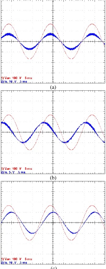
Initially, this prototype is operated in inversion mode to demonstrate its ability to cope with different power factors (unity, leading and lagging power factors).
The footprint of the tested prototype is shown in Fig. 13(a). To demonstrate the effectiveness of the integration design of L1 and L2 as discussed in section III, a low power integrated
magnetic inductor is built as shown in Fig. 13(b) and tested when one of its phases is operated as a single-phase standalone inverter from 50V DC-link without incorporation of second harmonic compensation loop. The voltage and current waveforms of the IBBC are shown in Fig. 14(a). The results in Fig. 14(b) have shown that the integrated design of the two inductors L1 and L2 is able to work independently in
one core without any noticeable performance degradation. Therefore, the magnetic integration technique is to be an effective solution in confine space applications where compact hardware design is preferred. Observe that the open loop output voltage and its spectrum in Fig. 15 exhibit certain amount of second order harmonic, which is in line with the previous analysis. In Fig. 15(a),the zero-crossing point drifts by 0.4ms and 3.7% of second harmonic can be observed from
Fig. 15(b).This distortion is expected to be aggravated as the power increases, necessitating the incorporation of the second order harmonic mitigation mechanism within the converter control loop.
(a) (b)
Fig. 13 Photographs of (a). prototype for the power circuit of the proposed (three-phase) and its drivers and (b). integrated design of magnetic parts (L1 and L2).
(a)
[image:10.612.350.522.37.333.2](b)
Fig. 14 Voltage and current waveforms of the state variables (5ms/div): (a). IBBC inductor current (5A/div) and IBBC capacitor voltage (20V/div); (b). Voltage across the two windings in the integrated magnetic component (50V/div).
(a)
(b)
Fig. 15 Open loop output voltage with second order harmonic distortion: (a). output voltage waveform (20V/div, 2ms/div); (b). distribution of the base band harmonics.
[image:10.612.338.535.381.667.2] [image:10.612.49.288.575.673.2]and harmonic elimination is adopted. This time, the proposed converter is operated in a three-phase configuration.
Fig. 16 ADC synchronization for asymmetric ripple compensation.
(a)
[image:11.612.349.522.212.651.2](b)
Fig. 17 Output waveforms for Standalone inverter mode (2ms/div): (a). line-to-line voltage (100V/div); (b) line current under 22Ω resistive load (5A/div).
Fig. 16 shows the ADC synchronization scheme employed to compensate the asymmetric deviation from average value during positive and negative half cycles. rp and rn are the
reference values with 180 degree apart, while Sp and Sn are the
state variables accordingly. The ADC time tsa will cause some
drift from the mid-point. Since the voltage/current slopes in the positive half cycle and negative half cycle are asymmetric for the proposed ACVD converter, some DC bias will appear when micro-controller samples one point (multi-times) per switching cycle. In another word, sampling process must strictly obey the Shannon principle, which demands the sampling speed to be at least two times of switching frequency. Consequently, the ADC module is suggested to be
synchronized at double frequency of the PWM generator. In this way, the extra samples can compensate the asymmetric deviation from the actual value and eliminate the DC bias.
Fig. 17 shows the output line-to-line voltage and three-phase currents obtained from standalone operation of the proposed converter in inversion mode. The THD for the voltage and current waveforms in Fig. 17 that obtained from the FFT analysis are both lower than 1%, which are expected to meeting the IEEE and IEC harmonic standards. Besides, the peak line-to-line voltage of 295V is achieved from 200V DC-link, which is beyond the DC utilization of 0.866pu for conventional two-level VSC. This confirms the claim made in this paper regarding the extended output voltage range of the proposed converter.
(a)
(b)
(c)