1
Supporting Information
Integrated Terahertz graphene modulator with 100%
modulation depth
Guozhen Liang,
1Xiaonan Hu,
1Xuechao Yu,
1Youde Shen,
4Lianhe H. Li,
2Alexander Giles
Davies,
2Edmund H. Linfield,
2Houkun Liang,
3Ying Zhang,
3Qi Jie Wang
1,4,*1
OPTIMUS, School of Electrical and Electronic Engineering, Nanyang Technological University, 50 Nanyang Avenue, 639798 Singapore.
2
School of Electronic and Electrical Engineering, University of Leeds, Leeds LS2 9JT, UK.
3
Singapore Institute of Manufacturing Technology, Singapore.
4
CDPT, School of Physical and Mathematical Sciences, Nanyang Technological University, 50 Nanyang Avenue, 639798 Singapore.
*Email: qjwang@ntu.edu.sg
1.
Far field and optical mode of the concentric-circular-grating (CCG) QCL
The design of the concentric-circular grating follows the rule in Ref. 1, with the whole grating
structure starting from the center to the boundary being: 59.8/3/27.4/3/26.3/3/26.6/3/26.5/3/26.4/3/27.4/3/ 27.4/3/27.4/3/27.4/3/27.4/3/27.4/3/27.9/3/27.9/3/27.9/3/27.9/3/150 in µm, where the bold numbers indicate the slit region, and the underlined parts are connected by spoke structures to allow electrical
pumping of the active region below (Fig. 1 in main text).
The two-dimensional far field emission pattern of the device was measured by scanning a pyroelectric
detector on a spherical surface centered at the laser, as shown in Fig. S1a, where the (0, 0) position
represents the normal to the laser surface. According to the measured far-field pattern, the optical mode in
the laser cavity was identified as that in Fig.S1b and Fig. S1c. As shown, the optical mode is confined in
2
larger than that enclosed by the white dash circle (Fig. S1b) or line (Fig. S1c) since there is lateral current
spreading in the active region of typically ~ 20 µm.
From the measured optical mode, it can be deduced that the CCG QCL operates on the sixth-order
azimuthal mode1 although the design was targeted on the first-order mode. This deviation is mainly due to an underestimation of the gain peak frequency of the active region.
Figure S1. Far field and optical mode of the CCG QCL. a, Measured two-dimensional far-field emission pattern of the surface-emitting CCG QCL, where the (0, 0) position represents the normal to the
laser surface. b and c, Corresponding electric field (Ez) distributions of the laser in plan, and
cross-sectional views, respectively. The white dash line illustrates the electrically pumped area.
2.
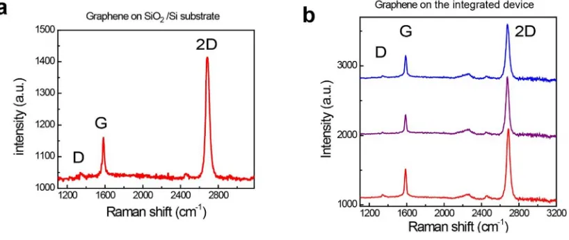
Raman Spectra of the transferrd graphene
Fig. S2a shows the Raman spectrum of the transferred graphene on the SiO2/Si substrate, and Fig.
S2b shows the Raman spectrum of the transferred graphene in different slits (apertures) of the
[image:2.612.127.489.217.442.2]3
2250cm-1 is likely from the chemical residue in the slits. Overall, the near absent D peak, single-Lorentzian-shape 2D peak and the 2D/G intensity ratio (~3) of each spectrum confirm the high quality of
the graphene after transfer.
Figure S2. Raman characterization of the transferred graphene. Raman spectra of the transferred graphene on a, a SiO2/p-Si substrate and b, in the slits of the CCG of the integrated device.
3.
Model used to retrieve the graphene parameters
The carrier density in the graphene can be approximately expressed by:2
2 2
0
(
)
tot g
n
=
n
+
n V
(1)Here
n
0represents the residual carrier concentration at the Dirac point, which is non-zero owing tocharged impurities in the dielectric or the graphene/dielectric interface.3 n V( g) represents the carrier
concentration induced by the electric gating, and can be obtained from a parallel capacitor model:
f g Dir
ox ox
E
e
e
V
V
n
n
c
e
c
[image:3.612.93.502.161.334.2]4 0
/
ox ox
c
=
ε ε
t
is the geometrical capacitance, withε
0 being the permittivity of free space andε
ox thedielectric constant of SiO2 (~3.9). For oxide thickness of t=450nm,
9 2
8 10 /
ox
c = × − F cm .
V
Dir is theapplied voltage corresponding to the Dirac point.
The square resistance across the source and drain is given by:2
1
tot contact tot
R R
en u
= + (3)
where
R
contact represents the metal/graphene contact resistance.By fitting the measured data with the above model, as shown in Fig. S3, we were able to extract the
following parameters: n0 =1.0 10 /× 12 cm2,
u
=
924
cm V s
2 −1 −1,V
Dir=
50.2
V
andR
contact=
440
Ω
.The graphene sheet conductivity in the main text is given by 1 /
(
Rtot(measured)−440Ω)
, theFermi level is calculated by
E
f=
h
ν
fπ
n
tot , where 6 11 10
f ms
ν
≈ × −is the Fermi velocity.4
[image:4.612.201.431.449.638.2]5
4.
Comparison of the graphene response at 78 K and 300 K
To investigate the graphene response at cryogenic and room temperature, we measured the electrical
transport and optical modulation of the same graphene sheet at 78 K and 300 K. As plotted in Fig. S4a, at
78 K, the graphene undergoes a larger change of conductivity across the gate voltage range. Treating the
graphene as a zero thickness conductive layer with free carriers and current, the transmission intensity at
the air/graphene/dielectric interface can be expressed as: 6
2 0 0
0
( , V )
1
( )
( , V )
1
( , V )
G diel
Dir diel G
T
n
Z
T
n
Z
ω
σ ω
ω
σ ω
+
+
=
+
+
(4)where
n
diel is the refractive index of the dielectric,Z
0=
376.73
Ω
is the vacuum impedance,σ ω
0( )
and
σ ω
( , V )
G are the graphene optical conductivity at the Dirac point and VG gate voltage, respectively.The optical conductivity
σ ω
( , V )
G is related to the DC conductivityσ
(V )
G measured electrically by(
2 2)
( , V )G (V ) / 1G
σ ω
=σ
+ω τ
, withτ
being the carrier momentum scattering time (~15 fs).4,5 Thecalculated T(Vg)/TCNP - VG curves of the THz radiation (at ~3.2 THz) at the air/graphene/SiO2 interface
are also plotted in Fig. S4, showing a slightly higher modulation depth (~1%) at 78 K than that at 300 K.
6 Figure S4. Comparison of the graphene response at 78 K and 300 K. a, Calculated transmittance normalized to the value at the Dirac point and the electrical transport measurements of the graphene sheet
at 78 K and 300 K. b, Modulation of the THz radiation by the graphene at 78 K and 300 K with the effect of the Si substrate removed. Before removing this substrate effect, the modulation depth is higher (17%).
5.
High-frequency circuit model of the graphene modulator
To investigate the high speed performance of the integrated modulator, we constructed an equivalent
circuit model. Fig. S5a present the schematic of the modulation scheme, a function generator with output
internal impedance R0 = 50 Ω is placed between the two electrodes that are insulated by the SiO2 layer.
The main components that affect the high frequency performance of the integrated modulator are shown
in Fig. S5b, with the cross-section view shown schematically in Fig. S5c. The slits are numbered as 1, 2,
3, ... , . The circuit model for a single slit marked by a dashed box is also shown, where RLG and R R
G are
respectively the resistance of the graphene sheet from the left and right contact edge to the center of the
[image:6.612.96.494.75.237.2]7
G
C
is the capacitance between the graphene sheet and the back gate. This circuit can be simplified to thatin the lower right model in Fig. S5c, where the parameters can be written as:
/ 2 1
1 / 1 / 4
c
G L R
G G
d R
R R r
ρ
σ
π
+= ≈
+ (5)
0
(2
)
L R oxG p p
rd
C
C
C
t
ε ε
π
=
+
=
(6)Here,
ρ
cis the contact resistance across the metal/graphene edge in units ofΩ⋅
µ
m
,σ
is the grapheneconductivity, ris the distance from the center of the slit to the center of the device,
t
is the thickness ofthe SiO2 (450 nm),
d
is the width of the slit (14 µm),ε
0 is the vacuum permittivity andε
ox is therelative permittivity of the SiO2.
The slits are in parallel in the circuit, and therefore the equivalent circuit for the whole modulator is as
shown in Fig. S5d. From the previous two equations, we have
1 2 6
1 2
...
6G G G
G G G
R
R
R
C
=
C
= =
C
. (7)This means the voltages at the red points in Fig. S5d are equal, and we can therefore simplify the circuit
model to the one shown in Fig. S5e, where:
1 2 6
1 2 6
4 4
/ 2
1
1
(
)
1/
1/
... 1 /
4
...
2 10
10
180
t c
G
G G G
c
d
R
R
R
R
r
r
r
um
ρ
σ
π
ρ
σ
−+
=
=
+
+ +
+ + +
×
≈
+
≈
Ω
(8) 2 01 2 6
1 2 6
2
...
(
...
)
6.5
SiO t
G G G G
d
C
C
C
C
r
r
r
8
2 0
1 2 6
...
8.7
SiO p t
p p p p
A
C
C
C
C
t
pF
ε ε
=
+
+ +
=
≈
(10) pA is the total area of the graphene contact for slits 1 to 6. In equation (8),
(
/ 2)
(440
/ 2) 8000
c
R
contactl
contactum
ρ
=
×
≈
Ω
×
, whereR
contact is the contact resistance obtained inSection 3, and
l
contact is the length of the graphene/metal edge of the separated device. Based on thecircuit model, the applied gate voltage can be calculated as:
0 in p S in Z V V Z R = ×
+ (11)
Where
Z
in is the total impedance of the modulator, enclosed by the dashed box in Fig. S5e, and can bewritten as:
(1/
) (1 /
)
(1/
) (1/
)
t t t
G G p
in t t t
G G p
R
i C
i C
Z
R
i C
i C
ω
ω
ω
ω
+
=
+
+
. (12)Here
ω
=
2
π
f
withf
being the frequency of the modulation signalV
S. The signal that actually drivesthe carriers in and out of the graphene is
0
0 0
1 1
1 1
1 / ( 1 / ) 1
in
G S t t
in G G
S t t t t t
p G G G G
Z
V V
Z R i R C
V
i R C R R i C i R C
ω
ω
ω
ω
= × ×
+ +
= × ×
+ + + +
(13)
To characterize the high-frequency response of the integrated modulator, we have performed an
S-parameter measurement using a radio frequency (RF) network analyzer. The dynamic response (S21) is
9 21
0
2 2
in in
Z S
Z R
=
+ (14)
Combining equations (12) – (14), we get
21
1 1
2 / 1 1
G S t t
G G
V V
S i R C
ω
= × ×
− + (15)
Using the estimated values RGt ≈180Ω , and CGt ≈6.5pF , we are able to plot the normalized
modulation depth (VG/VS) of the electrical signal applied to the graphene sheet as a function of the
modulation frequency (black circular symbol in Fig. S6). The estimated 3-dB cutoff frequency is 110
10 Figure S5. Equivalent circuit model of the integrated graphene modulator. a, Schematic of the modulation scheme, the internal impedance of the function generator is R0 (50 Ω). b, Principal
components that affect the high speed performance of the integrated modulator. c, cross-section view of modulator in b, and the equivalent circuit for a single slit. d, equivalent circuit for the whole modulator. e, simplified circuit model for the modulator.
Figure S6. Frequency response of the integrated graphene modulator measured by an RF network analyzer. The blue triangular symbol represents the S21 response of the device and the black circular
[image:10.612.163.461.186.414.2]11
Reference
(1) Liang, G.; Liang, H.; Zhang, Y.; Li, L.; Davies, A. G.; Linfield, E.; Yu, S. F.; Liu, H. C.; Wang, Q. J. Low Divergence Single-Mode Surface-Emitting Concentric-Circular-Grating Terahertz Quantum Cascade Lasers. Opt. Express2013, 21, 31872.
(2) Kim, S.; Nah, J.; Jo, I.; Shahrjerdi, D.; Colombo, L.; Yao, Z.; Tutuc, E.; Banerjee, S. K. Realization of a High Mobility Dual-Gated Graphene Field-Effect Transistor with Al2O3 Dielectric. Appl. Phys. Lett.
2009, 94, 062107.
(3) Adam, S.; Hwang, E. H.; Galitski, V. M.; Das Sarma, S. A Self-Consistent Theory for Graphene Transport. Proc. Natl. Acad. Sci. U. S. A.2007, 104, 18392–18397.
(4) Lee, S. H.; Choi, M.; Kim, T.-T.; Lee, S.; Liu, M.; Yin, X.; Choi, H. K.; Lee, S. S.; Choi, C.-G.; Choi, S.-Y.; Zhang, X.; Min, B. Switching Terahertz Waves with Gate-Controlled Active Graphene
Metamaterials. Nat. Mater.2012, 11, 936–941.
(5) Valmorra, F.; Scalari, G.; Maissen, C.; Fu, W.; Schönenberger, C.; Choi, J. W.; Park, H. G.; Beck, M.; Faist, J. Low-Bias Active Control of Terahertz Waves by Coupling Large-Area CVD Graphene to a Terahertz Metamaterial. Nano Lett.2013, 7,3193-3198.
(6) Saleh, B. & Teich, M. Fundamentals of Photonics, 2nd edn, Wiley, New York, 2007.